Mechanical Decoupling of Quantum Emitters in Hexagonal Boron Nitride from Low-Energy Phonon Modes
Abstract
Quantum emitters in hexagonal Boron Nitride (hBN) were recently reported to hold a homogeneous linewidth according to the Fourier-Transform limit up to room temperature. This unusual observation was traced back to decoupling from in-plane phonon modes which can arise if the emitter is located between two planes of the hBN host material. In this work, we investigate the origins for the mechanical decoupling. Improved sample preparation enabled a reduced background and a 70-fold decrease of spectral diffusion which was so far the major drawback of defect center in hBN and allowed us to reveal a gap in the electron-phonon spectral density for low phonon frequencies. This decoupling from phonons persists at room temperature and explains the observed Fourier Transform limited lines up to 300K. Furthermore, we investigate the dipole emission directionality and show a preferred photon emission through the side of the hBN flakes supporting the claim for an out-of-plane distortion of the defect center. Our work lays the foundation to a deeper understanding of the underlying physics for the persistence of Fourier-Transform limit lines up to room temperature. It furthermore provides a description on how to identify the mechanically isolated emitter within the large number of defect centers in hBN. Therefore, it paves the way for quantum optics applications with defect centers in hBN at room temperature.
I Introduction
Fourier-Transform limited (FTL) transitions in atomic systems are among the most crucial ingredients for many quantum optics experiments Legero et al. (2004); Moehring et al. (2007); Lettow et al. (2010); Togan et al. (2010); Sipahigil et al. (2012); Ritter et al. (2012); Bernien et al. (2013); Sipahigil et al. (2014). Furthermore, they might become key building blocks for future large-scale quantum networks Kimble (2008); Sipahigil et al. (2016); Wehner et al. (2018). Until recently, the systems exhibiting such transitions, where the spectral width is solely determined by the excited state lifetime, can be divided in two categories. First, atomic systems such as neutral atoms Kuhn et al. (2002); Darquié et al. (2005); Thompson et al. (2006) or ions Maunz et al. (2007); Barros et al. (2009); Almendros et al. (2009) that operate at room temperature but with a large technical overhead and with limited rates. Second, atom-like solid state systems that can be operated in compact setups and at high rates but with the requirement for cryogenic temperatures in order to suppress electron-phonon interaction with the solid-state environment Sipahigil et al. (2012, 2014); Sapienza et al. (2015); Kuhlmann et al. (2015); Jahn et al. (2015); Chu et al. (2017); Bhaskar et al. (2017); Dietrich et al. (2018).
In the past few years, a new atom-like system has emerged, namely defect centers in hexagonal Boron Nitrite (hBN) Tran et al. (2016a); Toth and Aharonovich (2019). The emitter evidence extraordinary optical Grosso et al. (2017); Noh et al. (2018); Proscia et al. (2018); Tran et al. (2018); Dietrich et al. (2018); Konthasinghe et al. (2019); Nikolay et al. (2019) and spin Exarhos et al. (2019); Gottscholl et al. (2020); Chejanovsky et al. properties. In addition, first steps towards integrating quantum emitters in hBN into photonic devices were successfully tested Schell et al. (2017); Tran et al. (2017); Kim et al. (2018); Vogl et al. (2019). A very unique and remarkable feature is the persistence of FTL lines up to room temperature Dietrich et al. (2020). The unusual persistence of the optical transition against interaction with its solid-state environment was traced back to decoupling from in-plane phonon modes under resonant excitation. However, besides the introduction of a consistent model the experimental proof for the mechanical decoupling is lacking.
In this work, we shed light on new physics based on a quantum emitter which is trapped between two layers of the hBN host. We explain the underlying mechanism of the mechanical decoupling by a systematic spectroscopic study of the excitation and emission properties. At low temperatures we extract the electron-phonon spectral density at low frequencies and examine the persistence of the mechanical isolation up to room temperature. We embed our observations into a consistent theoretical model. In the last paragraph, we analyze the topology of different hBN flakes via AFM microscopy and confirm that all defect centers which are mechanical decoupled emit photons in parallel to the hBN layer orientation. The emission directionality is consistent with a dipole that is distorted out-of-plane. Our work not only gives valuable insights into the new physics of mechanical isolation of defect center in hBN. It also gives a guideline to the community on how to identify those emitters. We therefore contribute important steps to utilize defect center in hBN in quantum optics applications that can be operated at room temperature.
II Results
II.1 Spectral properties
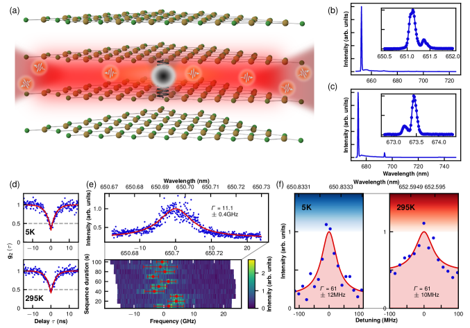
As illustrated in figure 1(a), our proposed model for explaining the persistence of Fourier-Transform limited lines up to room temperature rests upon mechanical decoupling of the optical transition from phonon modes in the hBN lattice Dietrich et al. (2020). Emitters located between hBN layers may be the cause of this decoupling because their orbitals are less susceptible to in-plane phonon distortions. In order to understand the underlying mechanism, we first measure the photoluminescence (PL) spectrum as input for a phonon sideband decomposition model. This allowed us to extract the electron-phonon spectral density and associate its resonances to hBN phonon modes. We then in turn utilize resonant excitation of phonon resonances to investigate the coupling of the modes under resonant drive. Since our laser system (Sirah Matisse 2 DS) operates in a wavelength range limited to 618 - 671 nm, we focus on two emitters where one, emitter A (see fig. 1(b)), can be excited resonantly and near resonantly to the zero phonon line (ZPL) and the second one, emitter B (see fig. 1(c)), can be excited further away (up to 56 nm) from the ZPL via the optical phonon mode. Emitter A features a ZPL at a wavelength of 651nm. Its PL spectrum shows a low background fluorescence and high signal intensity. We measure the second order autocorrelation function in Hanbury-Brown and Twiss (HBT) configuration to verify the single photon character of our emitters. The thereby arising relatively high value of (see fig. 1(d)) originates from a second, uncorrelated ZPL, as reported previously in Bommer and Becher (2019). At room temperature, this value rises to due to higher background fluorescence. As observed in the PL spectrum at 5K, the latter ZPL is only 0.25 nm detuned and five times less intense than the main ZPL (see fig. 1(b)). Nevertheless, the single photon character is clearly proven for 5K and 295K since . Fitting the second order correlation function
| (1) |
to data from a correlation measurement yields a natural linewidth of at cryogenic and at room temperature, in line with previous reports Tran et al. (2016b); Sontheimer et al. (2017); Tran et al. (2018). The excitation power is kept well below saturation in order to avoid power broadening. For further analysis it is important to note that the contribution of the second emitter to the phonon sideband (PSB) emission is small. Next, we perform resonant photo luminescence excitation spectroscopy (PLE) by scanning the laser frequency over the emitter transition frequency with a tunable dye laser. The Lorentzian fit to the resonance, as illustrated in 1(e), yields an inhomogeneous linewidth at 5K of hinting to residual spectral diffusion. Compared to earlier works Dietrich et al. (2020), we iteratively improved our sample preparation process, resulting in clean emitter spectra and low background fluorescence. Furthermore, the cleaner substrate with less surface disturbances reduces spectral broadening and stabilizes the emitter. Thus, we could improve the inhomogeneous linewidth by a factor of 70 at comparable excitation powers of few . For individual scans we encounter a homogeneous linewidth within the FTL of . An exemplary scan at cryogenic temperature (5K), reveals a homogeneous linewidth of , as shown in Fig. 1(f). At room temperature (293K), a scan with a measured linewidth of (see Fig. 1(f)) confirms the FTL of the homogeneous linewidth.
II.2 Phonon sideband decomposition
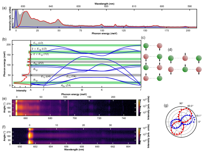
Now, we study the PL spectrum of emitter A in detail to identify the defect’s electron-phonon coupling mechanisms. In figure 2(a), the blue curve shows the defect’s bright ZPL emission. The grey shaded intensity shows a magnified view of the PSB which highlights the phonon features. We applied a PSB decomposition method which adopts a linear symmetric mode model Davies (1974); Kehayias et al. (2013); Balasubramanian et al. (2019) to describe the PSB in terms defect’s electron-phonon spectral density, also referred to as the one-phonon band. The one-phonon band represents all defect processes involving the creation and/or annihilation of a single phonon. Using our method we accurately decomposed the PSB into its one-phonon band. Further details of the decomposition process are included in the supplemental material 111see supplemental material. Since the band can be accurately modeled in terms of its one-phonon band, we can assume the absence of strong vibronic interactions that involve non-symmetric modes or introduce anharmonic effects, like Jahn-Teller.
Next, we compare the intensities of the one-phonon band features to the intrinsic phonon modes of hBN to identify the defect’s electron-phonon processes. Here we are assuming that the emitter does not significantly perturb the modes of pristine hBN. Features in the one-phonon band correspond to frequencies of high mode density and/or where there is strong coupling to the defect orbitals. The one-phonon band is plotted against the phonon band structure of pristine hBN as shown in figure 2(b). The modes that couple to the defect are highlighted in green. The one-phonon band’s largest feature is a broad peak centered at 11meV. The prominence of this feature indicates that, at this frequency, two things are occurring: a high density of modes and strong coupling to the defect. The feature is coincident with the leveling out of the and bands at the -point. These are acoustic modes in the out-of-plane direction, their qualitative atomic displacements are shown in Fig. 2(c). The -point corresponds to out-of-plane wave-vector at the edge of the Brillouin zone. This means that -point phonons also result in maximum displacement between equivalent atoms in neighboring unit cells in the inter-plane direction. There is a sharp feature at 50meV that does not coincide with any critical points in the band-structure, indicating that it is a local mode. The next green peak corresponds to the mode at the -point, which is the out-of-plane optical mode in Fig. 2(d). The feature at 115meV does not coincide with any band structure detail, since it stems from the Raman line of chromium defects in the sapphire substrate and not from the emitter itself.
The remaining features of the one-phonon band imply that the defect weakly couples to the following: (1) the longitudinal acoustic mode at the -point, (2) potentially multiple transverse modes, and (3) the longitudinal optical mode at the -point. These modes correspond to in-plane displacements between neighboring unit cells of hBN. The microscopic displacements that can be associated to the last three features are quite complicated. As a result, it is not immediately obvious how they may interact with the defect. Nevertheless, these observations may still provide some insight as we develop our understanding of the defect.
Given the defect’s strong coupling to modes that result in out-of-plane displacements, we conclude that the orbitals of the defect exist between the layers of hBN. This is consistent with the picture presented in Dietrich et al. (2020) that an out-of-plane distortion has led to decoupling from in-plane phonons. We generalize the result to other interplane defects like a trapped atom near an impurity or vacancy.
The polarization-dependent PL spectrum shown in figures 2(e) and (f), exhibits the polarization of the full PSB. Light emitted from the ZPL shows a distinct polarization contrast. Thereto, the polarization contrast for the off-resonant excitation at 532nm is rotated by 41°(see Fig 2(g)), as observed previously Jungwirth et al. (2016) and hinting towards an additional excited state. The polarization of both the optical phonon mode at 710nm and the low-energy acoustic phonon modes are aligned to the ZPL emission. We conclude that the involvement of phonons in the emission process does not alter the polarization contrast. This is consistent with the defect coupling to linear symmetric modes.
II.3 Coupling to excited state phonon sideband
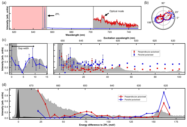
Next, we probe the electron-phonon coupling strength of individual phonon resonances. For this purpose we utilize wavelength-dependent PLE spectroscopy. We operate the experiment in two different modes. First, we integrate the spectrum over the optical phonon sideband from 705nm to 800nm, as illustrated in Fig. 3(a), in order to detect the fluorescence when exciting close to the ZPL. Second, we use the integral of a Gaussian fit to the ZPL as intensity measure when exciting further away from the ZPL. Thereby, we can measure the excitation strength over a large frequency range and compare it to the PL signal when adjusting the scaling of the emitter intensity. The first observation is that we can clearly excite the first phonon feature, which can be associated to the first ZA mode, 8 meV detuned from the ZPL. The polarization contrast of the excitation on-resonance with the acoustic mode yields the polarization-dependence as depicted in Fig. 3(b). In contrast to the polarization of the off-resonant excitation at 532nm we now observe the excitation polarization aligned to the ZPL emission polarization. We conclude that we are now addressing the same excited state with a ZA-phonon-assisted excitation that preserves the polarization. Figure 3(c) unfolds the polarization- and wavelength-dependent electron-phonon coupling across the complete phonon spectrum. We note, that there is also a weak excitation probability on-resonance with the ZA mode but with perpendicular polarization with respect to the ZPL emission. We interpret this observation as residual excitation of the second, much weaker ZPL. Since that second ZPL of both defects is detuned by around 0.8meV (see insets in figs. 1(b) and (c)), we do not resolve the splitting here. Now, we want to investigate the low-frequency gap between the ZPL and the acoustic phonon branches and therefore focus on the data polarized parallel to the ZPL emission. The fluorescence intensity and therefore the electron-phonon coupling strength displays a clear minimum at about 5meV detuned from the ZPL confirming our findings in PL spectroscopy. The maximum on-resonance with the first acoustic phonon energy at around 8 meV detuned from the ZPL resonance at 0 meV also agrees with the results from the PL spectrum. The left panel in figure 3(c) illustrates the gap width for both, PL and PLE data. Therefore, we determine the peak positions of ZPL and PSB, respectively, and define the gap size as their difference. The figure illustrates the consistency of the gap width between PL and PLE measurement.
We now finalize our study of the electron-phonon coupling strength by investigating the optical phonon mode. Due to electromagnetic coupling between the optical transition and the optical mode we expect electron-phonon coupling even for an emitter that is displaced out-of-plane of the hBN layer. Due to the limited tuning range of our laser system we use a second emitter B with a ZPL at 673nm to probe excitation via the optical phonon mode. The PL spectrum and the wavelength-dependent excitation is shown in figure 3(d). The emitter can be excited efficiently via the optical phonon mode showing a distinct resonance at 165meV detuned from the ZPL and in agreement with previous results Wigger et al. (2019). The polarization of the excitation laser is again aligned with the polarization of the ZPL emission confirming that the phonon-assisted excitation does not alter the polarization properties. Please note, that also in this case we do observe a second ZPL with an intensity of approximately half of the first ZPL. That ZPL could explain the residual excitation probability perpendicular to the ZPL emission. Furthermore, please note that we observe signs of additional modes in excitation at a detuning of approximately 75 meV from the ZPL. However, assigning these resonances to modes in the PL spectrum is not distinct.
II.4 Temperature dependent gap size
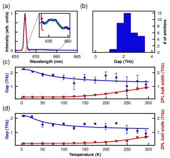
In the following, we focus on the temperature dependence of the gap in the electron-phonon spectral density and its persistence up to room temperature. We extrapolate the gap size by fitting a Gaussian to the ZPL and to the first acoustic phonon feature and determine the gap size as distance between both peaks. An example is illustrated in Fig. 4(a). A characterization of 33 different emitters yields an average gap size of about 2 THz within a distribution of approximately 1 THz, as illustrated in Fig.4(b). The histogram is asymmetric and drops faster towards smaller gap size since smaller gap widths are more difficult to resolve. In order to be able to observe the gap its size needs to be larger than the ZPL linewidth. We characterize both, the gap size of emitter A and B for different temperatures from 5 K to 300 K, as plotted in Fig. 4(c) and (d), respectively and plot it against the ZPL linewidth. With rising temperature the gap size narrows whereas the width of the ZPL increases. The gap of both emitters remains open and observable all the way to room temperature. However, the gap size at 300 K decreases to about half the size at 5 K while the ZPL width increases to almost half the gap size at 300 K. We fit the temperature dependence of both, the ZPL linewidth and the gap size, with the Boltzmann function
| (2) |
with denoting the gap size or the ZPL width and the fit constants , and and extrapolate a gap size of THz at 294.2 K with a ratio for the Boltzmann energy of . This dependence could arise from a temperature-dependent distortion that modifies the electron-phonon couplings and phonon frequencies. For example, this could be a further out-of-plane distortion of an already distorted defect or changes to the configuration of an inter-plane defect. For changes in the electron-phonon coupling to shift the energies of PSB features, there must be a difference in the phonon frequencies between the two electronic levels of the optical transition. This is a higher order effect that is not captured by the linear symmetric mode model and warrants future investigation.
II.5 AFM flake characterization
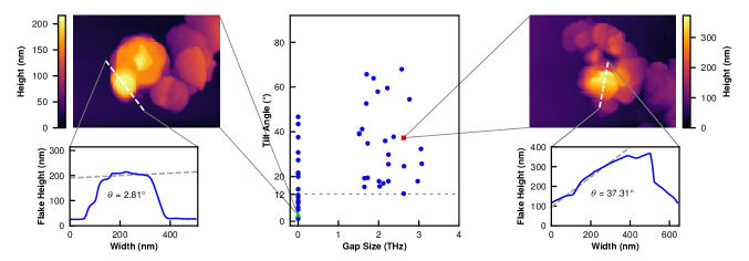
Finally, we characterize the topology of the hBN flakes with an atomic force microscope (AFM). We compare the flake texture between flakes hosting emitters with and without gap in the electron-phonon density of states. The AFM scan of the height profile reveals the angle of the hBN flake surface with respect to the substrate surface, which we equalize to the hBN layer orientation. Two exemplary scans are shown in figure 5. We now gain insights into the mechanical decoupling mechanism by correlating the tilt angle of the hBN flakes hosting the defect centers with the gap size observed in the PL spectrum. If an out-of-plane distortion of the emitter is the origin for the mechanical decoupling, then all emitters with a gap should only be observable in tilted hBN flakes. In contrast, all emitters without a gap should predominantly be observed in hBN flakes lying flat on the surface corresponding to small tilt angles. This correlation is clearly visible in figure 5. In total 45 emitters are studied. All emitters with no gap in the PL spectrum are observed in hBN flakes with a tilt angle below 50°. In fact every second flake has a tilt of less than 12°. Vice versa, all flakes hosting emitters with a gap in the PL spectrum yield tilt of at least 12°. Possibly, the dipole of emitters with gap is distorted out-of-plane and the emission tends to spread along the hBN layers. This results in a better visibility when the flake is tilted such that the hBN layers and the emitted light points towards the objective for collection. On the other hand, in-plane defects result in gapless emitters. Since their dipoles are also located in-plane the emission is mostly perpendicular to the hBN layers. We observe this class of emitters in flakes with small tilt angles.
III Conclusions
In summary, we confirm that some defect center in hBN exhibit mechanically decoupled electronic transitions under resonant excitation. Improved sample preparation enabled a 70-fold decrease in spectral diffusion and allowed us in this work to observe a gap of around 2 THz in the electron-phonon density of states which remains open up to room temperature. In a systemic study of the coupling to individual modes we developed a model where the emitter has orbitals that exist between the layers of hBN. This model was proposed in reference Dietrich et al. (2020) to explain the persistence of FTL linewidths in resonant excitation up to room temperature. We furthermore categorize common features of all emitters with decoupled optical transitions showing a gap in the PL and wavelength-dependent PLE spectrum between ZPL and first acoustic phonon modes. Our results imply that only multilayer hBN flakes can serve as host for this emitter type. Furthermore, the emission directionality is shifted towards an emission parallel to the hBN layer. Besides new insights into the physics explaining the extraordinary observation of Fourier-transform limited lines at room temperature our work also outlines a catalog that could be used in future experiments to identify mechanically decoupled emitters. Our work therefore opens up new ways to use defect center in hBN for quantum optics applications at room temperature.
Acknowledgements.
The project was funded by the Deutsche Forschungsgemeinschaft (DFG, German Research Foundation) - Project number: 398628099. A.K. acknowledges support of the European fund for regional development (EFRE) program Baden-Württemberg. M.W.D. acknowledges support from the Australian Research Council (DE170100169). K.G.F. and A.K. acknowledge support of IQst. M.H. acknowledges support from the Studienstiftung des deutschen Volkes. The AFM was funded by the DFG. We thank Prof. Kay Gottschalk and Frederike Erb for their support. The Qudi software suite Binder et al. (2017) was used for running the experiment setup.References
- Legero et al. (2004) T. Legero, T. Wilk, M. Hennrich, G. Rempe, and A. Kuhn, Quantum beat of two single photons, Phys. Rev. Lett. 93, 070503 (2004).
- Moehring et al. (2007) D. L. Moehring, P. Maunz, S. Olmschenk, K. C. Younge, D. N. Matsukevich, L. M. Duan, and C. Monroe, Entanglement of single-atom quantum bits at a distance, Nature 449, 68–71 (2007).
- Lettow et al. (2010) R. Lettow, Y. L. A. Rezus, A. Renn, G. Zumofen, E. Ikonen, S. Götzinger, and V. Sandoghdar, Quantum interference of tunably indistinguishable photons from remote organic molecules, Phys. Rev. Lett. 104, 123605 (2010).
- Togan et al. (2010) E. Togan, Y. Chu, A. Trifonov, L. Jiang, J. Maze, L. Childress, G. Dutt, A. Sørensen, P. Hemmer, A. Zibrov, and M. Lukin, Quantum entanglement between an optical photon and a solid-state spin qubit, Nature 466, 730 (2010).
- Sipahigil et al. (2012) A. Sipahigil, M. L. Goldman, E. Togan, Y. Chu, M. Markham, D. J. Twitchen, A. S. Zibrov, A. Kubanek, and M. D. Lukin, Quantum interference of single photons from remote nitrogen-vacancy centers in diamond, Phys. Rev. Lett. 108, 143601 (2012).
- Ritter et al. (2012) S. Ritter, C. Nölleke, C. Hahn, A. Reiserer, A. Neuzner, M. Uphoff, M. Mücke, E. Figueroa, J. Bochmann, and G. Rempe, An elementary quantum network of single atoms in optical cavities, Nature 484, 195 (2012).
- Bernien et al. (2013) H. Bernien, B. Hensen, W. Pfaff, G. Koolstra, M. Blok, L. Robledo, T. Taminiau, M. Markham, D. Twitchen, L. Childress, and R. Hanson, Heralded entanglement between solid-state qubits separated by three metres, Nature 497 (2013).
- Sipahigil et al. (2014) A. Sipahigil, K. D. Jahnke, L. J. Rogers, T. Teraji, J. Isoya, A. S. Zibrov, F. Jelezko, and M. D. Lukin, Indistinguishable photons from separated silicon-vacancy centers in diamond, Phys. Rev. Lett. 113, 113602 (2014).
- Kimble (2008) H. Kimble, The quantum internet, Nature 453, 1023 (2008).
- Sipahigil et al. (2016) A. Sipahigil, R. E. Evans, D. D. Sukachev, M. J. Burek, J. Borregaard, M. K. Bhaskar, C. T. Nguyen, J. L. Pacheco, H. A. Atikian, C. Meuwly, R. M. Camacho, F. Jelezko, E. Bielejec, H. Park, M. Lončar, and M. D. Lukin, An integrated diamond nanophotonics platform for quantum-optical networks, Science 354, 847 (2016).
- Wehner et al. (2018) S. Wehner, D. Elkouss, and R. Hanson, Quantum internet: A vision for the road ahead, Science 362 (2018).
- Kuhn et al. (2002) A. Kuhn, M. Hennrich, and G. Rempe, Deterministic single-photon source for distributed quantum networking, Phys. Rev. Lett. 89, 067901 (2002).
- Darquié et al. (2005) B. Darquié, M. P. A. Jones, J. Dingjan, J. Beugnon, S. Bergamini, Y. Sortais, G. Messin, A. Browaeys, and P. Grangier, Controlled single-photon emission from a single trapped two-level atom, Science 309, 454 (2005).
- Thompson et al. (2006) J. K. Thompson, J. Simon, H. Loh, and V. Vuletić, A high-brightness source of narrowband, identical-photon pairs, Science 313, 74 (2006).
- Maunz et al. (2007) P. Maunz, D. L. Moehring, S. Olmschenk, K. C. Younge, D. N. Matsukevich, and C. Monroe, Quantum interference of photon pairs from two remote trapped atomic ions, Nature Physics 3, 538 (2007).
- Barros et al. (2009) H. G. Barros, A. Stute, T. E. Northup, C. Russo, P. O. Schmidt, and R. Blatt, Deterministic single-photon source from a single ion, New Journal of Physics 11, 103004 (2009).
- Almendros et al. (2009) M. Almendros, J. Huwer, N. Piro, F. Rohde, C. Schuck, M. Hennrich, F. Dubin, and J. Eschner, Bandwidth-tunable single-photon source in an ion-trap quantum network, Phys. Rev. Lett. 103, 213601 (2009).
- Sapienza et al. (2015) L. Sapienza, M. Davanço, A. Badolato, and K. Srinivasan, Nanoscale optical positioning of single quantum dots for bright and pure single-photon emission, Nature Communications 6, 7833 (2015).
- Kuhlmann et al. (2015) A. V. Kuhlmann, J. H. Prechtel, J. Houel, A. Ludwig, D. Reuter, A. D. Wieck, and R. J. Warburton, Transform-limited single photons from a single quantum dot, Nature Communications 6, 8204 (2015).
- Jahn et al. (2015) J.-P. Jahn, M. Munsch, L. Béguin, A. V. Kuhlmann, M. Renggli, Y. Huo, F. Ding, R. Trotta, M. Reindl, O. G. Schmidt, A. Rastelli, P. Treutlein, and R. J. Warburton, An artificial rb atom in a semiconductor with lifetime-limited linewidth, Phys. Rev. B 92, 245439 (2015).
- Chu et al. (2017) X.-L. Chu, S. Götzinger, and V. Sandoghdar, A single molecule as a high-fidelity photon gun for producing intensity-squeezed light, Nature Photonics 11, 58 (2017).
- Bhaskar et al. (2017) M. K. Bhaskar, D. D. Sukachev, A. Sipahigil, R. E. Evans, M. J. Burek, C. T. Nguyen, L. J. Rogers, P. Siyushev, M. H. Metsch, H. Park, F. Jelezko, M. Lončar, and M. D. Lukin, Quantum nonlinear optics with a germanium-vacancy color center in a nanoscale diamond waveguide, Phys. Rev. Lett. 118, 223603 (2017).
- Dietrich et al. (2018) A. Dietrich, M. Bürk, E. S. Steiger, L. Antoniuk, T. T. Tran, M. Nguyen, I. Aharonovich, F. Jelezko, and A. Kubanek, Observation of fourier transform limited lines in hexagonal boron nitride, Phys. Rev. B 98, 081414(R) (2018).
- Tran et al. (2016a) T. T. Tran, K. Bray, M. J. Ford, M. Toth, and I. Aharonovich, Quantum emission from hexagonal boron nitride monolayers, Nature Nanotechnology 11, 37 (2016a).
- Toth and Aharonovich (2019) M. Toth and I. Aharonovich, Single photon sources in atomically thin materials, Annual Review of Physical Chemistry 70, 123 (2019).
- Grosso et al. (2017) G. Grosso, H. Moon, B. Lienhard, S. Ali, D. K. Efetov, M. M. Furchi, P. Jarillo-Herrero, M. J. Ford, I. Aharonovich, and D. Englund, Tunable and high-purity room temperature single-photon emission from atomic defects in hexagonal boron nitride, Nature Communications 8, 705 (2017).
- Noh et al. (2018) G. Noh, D. Choi, J.-H. Kim, D.-G. Im, Y.-H. Kim, H. Seo, and J. Lee, Stark tuning of single-photon emitters in hexagonal boron nitride, Nano Letters 18, 4710 (2018).
- Proscia et al. (2018) N. V. Proscia, Z. Shotan, H. Jayakumar, P. Reddy, C. Cohen, M. Dollar, A. Alkauskas, M. Doherty, C. A. Meriles, and V. M. Menon, Near-deterministic activation of room-temperature quantum emitters in hexagonal boron nitride, Optica 5, 1128 (2018).
- Tran et al. (2018) T. T. Tran, M. Kianinia, M. Nguyen, S. Kim, Z.-Q. Xu, A. Kubanek, M. Toth, and I. Aharonovich, Resonant excitation of quantum emitters in hexagonal boron nitride, ACS Photonics 5, 295 (2018).
- Konthasinghe et al. (2019) K. Konthasinghe, C. Chakraborty, N. Mathur, L. Qiu, A. Mukherjee, G. D. Fuchs, and A. N. Vamivakas, Rabi oscillations and resonance fluorescence from a single hexagonal boron nitride quantum emitter, Optica 6, 542 (2019).
- Nikolay et al. (2019) N. Nikolay, N. Mendelson, E. Özelci, B. Sontheimer, F. Böhm, G. Kewes, M. Toth, I. Aharonovich, and O. Benson, Direct measurement of quantum efficiency of single-photon emitters in hexagonal boron nitride, Optica 6, 1084 (2019).
- Exarhos et al. (2019) A. L. Exarhos, D. A. Hopper, R. N. Patel, M. W. Doherty, and L. C. Bassett, Magnetic-field-dependent quantum emission in hexagonal boron nitride at room temperature, Nature Communications 10, 222 (2019).
- Gottscholl et al. (2020) A. Gottscholl, M. Kianinia, V. Soltamov, S. Orlinskii, G. Mamin, C. Bradac, C. Kasper, K. Krambrock, A. Sperlich, M. Toth, I. Aharonovich, and V. Dyakonov, Initialization and read-out of intrinsic spin defects in a van der waals crystal at room temperature, Nature Materials (2020).
- (34) N. Chejanovsky, A. Mukherjee, Y. Kim, A. Denisenko, A. Finkler, T. Taniguchi, K. Watanabe, D. Bhaktavatsala Rao Dasari, J. H. Smet, and J. Wrachtrup, Single spin resonance in a van der Waals embedded paramagnetic defect, arXiv:1906.05903 .
- Schell et al. (2017) A. W. Schell, H. Takashima, T. T. Tran, I. Aharonovich, and S. Takeuchi, Coupling quantum emitters in 2d materials with tapered fibers, ACS Photonics 4, 761 (2017).
- Tran et al. (2017) T. T. Tran, D. Wang, Z.-Q. Xu, A. Yang, M. Toth, T. W. Odom, and I. Aharonovich, Deterministic coupling of quantum emitters in 2d materials to plasmonic nanocavity arrays, Nano Letters 17, 2634 (2017).
- Kim et al. (2018) S. Kim, J. E. Fröch, J. Christian, M. Straw, J. Bishop, D. Totonjian, K. Watanabe, T. Taniguchi, M. Toth, and I. Aharonovich, Photonic crystal cavities from hexagonal boron nitride, Nature Communications 9, 2623 (2018).
- Vogl et al. (2019) T. Vogl, R. Lecamwasam, B. C. Buchler, Y. Lu, and P. K. Lam, Compact cavity-enhanced single-photon generation with hexagonal boron nitride, ACS Photonics 6, 1955 (2019).
- Dietrich et al. (2020) A. Dietrich, M. W. Doherty, I. Aharonovich, and A. Kubanek, Solid-state single photon source with fourier transform limited lines at room temperature, Phys. Rev. B 101, 081401 (2020).
- Bommer and Becher (2019) A. Bommer and C. Becher, New insights into nonclassical light emission from defects in multi-layer hexagonal boron nitride, Nanophotonics 8, 2041 (2019).
- Tran et al. (2016b) T. T. Tran, C. Elbadawi, D. Totonjian, C. J. Lobo, G. Grosso, H. Moon, D. R. Englund, M. J. Ford, I. Aharonovich, and M. Toth, Robust multicolor single photon emission from point defects in hexagonal boron nitride, ACS Nano 10, 7331 (2016b).
- Sontheimer et al. (2017) B. Sontheimer, M. Braun, N. Nikolay, N. Sadzak, I. Aharonovich, and O. Benson, Photodynamics of quantum emitters in hexagonal boron nitride revealed by low-temperature spectroscopy, Phys. Rev. B 96, 121202(R) (2017).
- Davies (1974) G. Davies, Vibronic spectra in diamond, Journal of Physics C: Solid State Physics 7, 3797 (1974).
- Kehayias et al. (2013) P. Kehayias, M. W. Doherty, D. English, R. Fischer, A. Jarmola, K. Jensen, N. Leefer, P. Hemmer, N. B. Manson, and D. Budker, Infrared absorption band and vibronic structure of the nitrogen-vacancy center in diamond, Phys. Rev. B 88, 165202 (2013).
- Balasubramanian et al. (2019) P. Balasubramanian, M. H. Metsch, P. Reddy, L. J. Rogers, N. B. Manson, M. W. Doherty, and F. Jelezko, Discovery of st1 centers in natural diamond, Nanophotonics 8, 1993 (2019).
- Note (1) See supplemental material.
- Jungwirth et al. (2016) N. R. Jungwirth, B. Calderon, Y. Ji, M. G. Spencer, M. E. Flatté, and G. D. Fuchs, Temperature dependence of wavelength selectable zero-phonon emission from single defects in hexagonal boron nitride, Nano Letters 16, 6052 (2016).
- Wigger et al. (2019) D. Wigger, R. Schmidt, O. D. Pozo-Zamudio, J. A. Preuß, P. Tonndorf, R. Schneider, P. Steeger, J. Kern, Y. Khodaei, J. Sperling, S. M. de Vasconcellos, R. Bratschitsch, and T. Kuhn, Phonon-assisted emission and absorption of individual color centers in hexagonal boron nitride, 2D Materials 6, 035006 (2019).
- Binder et al. (2017) J. M. Binder, A. Stark, N. Tomek, J. Scheuer, F. Frank, K. D. Jahnke, C. Müller, S. Schmitt, M. H. Metsch, T. Unden, T. Gehring, A. Huck, U. L. Andersen, L. J. Rogers, and F. Jelezko, Qudi: A modular python suite for experiment control and data processing, SoftwareX 6, 85 (2017).