Direct measurement of interfacial Dzyaloshinskii-Moriya interaction at the MoS2/Ni80Fe20 interface
Abstract
We report on a direct measurement of sizable interfacial Dzyaloshinskii-Moriya interaction (iDMI) at the interface of two-dimensional transition metal dichalcogenide (2D-TMD), MoS2 and Ni80Fe20 (Py) using Brillouin light scattering spectroscopy. A clear asymmetry in spin-wave dispersion is measured in MoS2/Py/Ta, while no such asymmetry is detected in the reference Py/Ta system. A linear scaling of the DMI constant with the inverse of Py thickness indicates the interfacial origin of the observed DMI. We further observe an enhancement of DMI constant in three to four layer MoS2/Py system (by 56) as compared to 2 layer MoS2/Py which is caused by a higher density of MoO3 defect species in the case of three to four layer MoS2. The results open possibilities of spin-orbitronic applications utilizing the 2D-TMD based heterostructures.
Dzyaloshinskii-Moriya interaction (DMI) Dzialoshinskii (1957); Moriya (1960) favors perpendicular alignment of neighboring spins in a ferromagnetic material. In competition with Heisenberg exchange interaction, the DMI can lead to the formation of stable chiral spin textures such as Néel type domain walls or skyrmions, Roessler, Bogdanov, and Pfleiderer (2006); Bode et al. (2007) which are potential candidates for memory and logic applications due to their efficient current-driven motion and smaller size. Parkin, Hayashi, and Thomas (2008); Parkin and Yang (2015); Tomasello et al. (2014) These chiral structures were first observed in bulk non-centrosymmetric B20 magnetic materials such as MnSi, Mühlbauer et al. (2009) and FeGe Yu et al. (2011) due to the inherent broken inversion symmetry in these materials. In ferromagnet/heavy metal (FM/HM) heterostructures, the large spin-orbit coupling of the HM and the broken inversion symmetry at the interface result in an interfacial Dzyaloshinskii-Moriya interaction (iDMI). Fert and Levy (1980); Yang et al. (2015) More recently, stable skyrmions are observed in thin-film heterostructures of FM/HM bilayers due to the presence of an iDMI. Husain et al. (2019); Jiang et al. (2017) The FM/HM bilayer structures are technologically advantageous since they provide the opportunity to control and manipulate skyrmion/domain walls using current-induced spin-orbit torques present in these systems. Hence, the quantification of DMI constant is important both for fundamental physics as well as for designing efficient FM/HM systems for applications. Several direct and indirect measurement techniques such as Brillouin light scattering (BLS) spectroscopy, Nembach et al. (2015); Di et al. (2015a, b); Belmeguenai et al. (2015); Stashkevich et al. (2015) domain wall velocity, Torrejon et al. (2014) magnetic force microscope measurements, Baćani et al. (2019) asymmetric hysteresis loop method, Han (2016) etc. have been developed to quantify the strength of DMI. However, the wave vector (k) dependent BLS measurements have been established as a direct and very reliable method of measuring the strength of DMI. Nembach et al. (2015); Di et al. (2015b); Chaurasiya et al. (2016, 2018)
A large section of BLS measurement of DMI are focused to the FM/HM systems, namely, Py/Pt, Nembach et al. (2015) Co/Pt, Belmeguenai et al. (2015) CoFeB/W, Chaurasiya et al. (2016) CoFeB/Ta,Chaurasiya et al. (2018) CoFe/Pt, Belmeguenai et al. (2016) and Ta/Co2FeAl/MgO Husain et al. (2019) systems. More recently higher DMI strength is reported for superlattices of [Co/Pd(111)] Davydenko et al. (2019) and [Ir/Fe/Co/Pt]. Raju et al. (2019) Apart from conventional HMs, recent results have shown the presence of iDMI Chaurasiya et al. (2019); Yang et al. (2018); Ajejas et al. (2018) in Graphene/FM bilayer structures. Generally, DMI scales with spin-orbit coupling strength in the material in contact with the FM layer. Fert and Levy (1980); Yang et al. (2015) Hence, the presence of DMI in the Graphene-based heterostructure was surprising, given the low intrinsic spin-orbit coupling strength of Graphene. These results were explained based on the Rashba effect originated at the Graphene-FM interface Yang et al. (2018); Ajejas et al. (2018) or due to the extrinsic spin-orbit coupling at the Graphene-FM interface. Chaurasiya et al. (2019) However, the magnitude of the DMI parameter for these Graphene-based two-dimensional (2D) material-heterostructures is significantly lower compared to the FM/HM systems. In order to enhance the DMI parameter in the 2D material-heterostructures, 2D transition metal dichalcogenides (TMDs) materials are very promising, since they possess larger intrinsic spin-orbit coupling compared to Graphene. In addition, the lack of inversion center Xiao et al. (2012) in the crystal structure of TMDs provides immense advantage, which is already utilized to obtain unconventional spin-orbit torques in 2D TMDs/FM systems. MacNeill et al. (2017); Shao et al. (2016); Guimaraes et al. (2018)
In this work, we report on the direct observation of a sizable DMI in a reasonably large area and few layer-MoS2/Ni80Fe20 (Py) heterostructures using BLS measurements. MoS2 is a layered TMD having large intrinsic spin-orbit coupling which leads to a giant spin splitting due to the absence of inversion symmetry. Zhu, Cheng, and Schwingenschlögl (2011) The measured DMI in this system is found to be larger compared to Graphene/Py system Chaurasiya et al. (2019); Yang et al. (2018); Ajejas et al. (2018) and having comparable magnitude as that of the FM/HM bilayer systems for the similar thickness of FM layer. Nembach et al. (2015); Chaurasiya et al. (2016, 2018); Belmeguenai et al. (2016) The linear dependence of the DMI with the inverse of Py thickness and the absence of DMI in the reference sample indicate that the DMI in this system originates from the interface of MoS2 and Py layer. We found larger DMI for three to four layer (L) MoS2/Py system compared to the 2L MoS2/Py, which is attributed to a higher density of MoO3 defect species in the 3-4L MoS2.
We use large-area 2L and 3-4L MoS2 grown on Si/SiO2 substrates by pulsed laser deposition (PLD) technique. The substrates are cleaned with standard chemical cleaning procedures followed by annealing at 700 ∘C in a vacuum chamber for out-gassing of all impurities before deposition of MoS2 thin-films. The MoS2 thin films are then deposited using a 248 nm KrF excimer laser source at 5 Hz repetition frequency, 20 ns pulse width and 0.5 J/m2 energy density. The base pressure of Torr is maintained throughout the deposition process. The thickness of MoS2 was varied by the number of laser shots. The laser shots of 40 and 60 are optimized for 2L (layer) and 3-4L MoS2 growth, respectively. More details of MoS2 growth along with the characterization of bare MoS2 can be found in Ref Barvat et al., 2017. The Py and the Ta layers were grown in a separate DC magnetron sputtering chamber with a base vacuum of Torr after cleaning MoS2 samples with acetone and isopropyl alcohol. The Py thickness () was varied from nm while the Ta capping layer thickness was fixed at 2 nm. The bilayer metallic films are deposited at room temperature with a working pressure of Torr. A set of reference samples i.e., Py ()/Ta (2 nm) were also prepared simultaneously for comparison. The growth rate of Py and Ta thin-films were maintained at 1.43 /s and 1.83 /s, respectively.
The BLS measurements have been carried out in Damon-Eshbach (DE) geometry using a Sandercock type 3+3 pass Tandem Fabry-Pérot interferometer. Conventional 180° back scattered protocol along with the tool for wave vector selectivity was followed. As BLS relies on the inelastic light scattering process where total momentum is conserved in the plane of the thin film, Stokes (anti-Stokes) peaks are observed in the BLS spectra which correspond to the creation (annihilation) of magnons with momentum =sin, where = 532 nm in our case and is the angle of incidence of the laser beam. A well defined BLS spectrum was obtained after counting photons for several hours. Chaurasiya et al. (2016, 2019) In the DE geometry, the external magnetic field is applied perpendicular to the plane of incidence of the laser beam. This geometry allows the probing of the spin-waves propagating along the in-plane direction perpendicular to the externally applied field. More details of the BLS measurements can be found elsewhere. Chaurasiya et al. (2019, 2016, 2018)
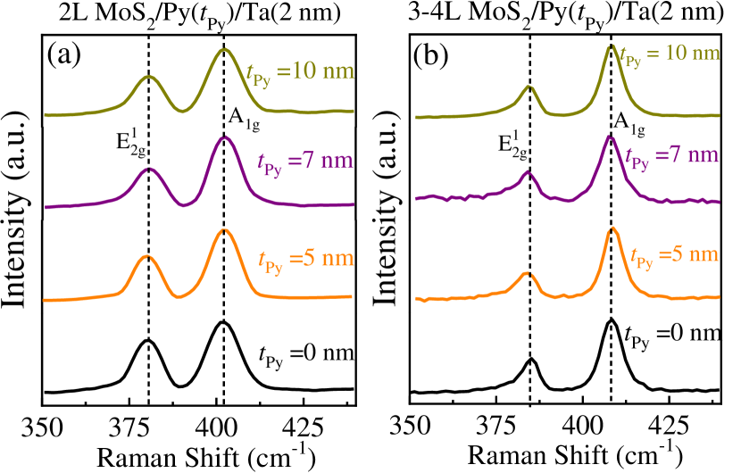
Figure 1 shows the Raman measurements performed on both bare 2L and 3-4L MoS2 and after deposition of Py/Ta for varying thicknesses of Py. Two peaks observed at 383 cm-1 and 408 cm-1 are the fingerprints of MoS2 and correspond to the E and modes, respectively. The observed difference in peak position of E and modes, denoted as is widely used as a reliable method of determining layer thickness for MoS2. Li et al. (2012) With the increasing number of layers, the E mode shifts to lower frequencies, while the mode shifts to higher frequencies. For the Raman spectra shown in Fig. 1(a), cm-1 is consistent with 2 layers of MoS2, while for the Raman spectra shown in Fig. 1(b), we found cm-1 which corresponds to three to four layers of MoS2. The difference , we report here, is the average of all the 2L and 3-4L MoS2 samples, since no significant differences in the values of were observed as a function of the Py thickness. These Raman measurements also show that the quality of MoS2 layer remains unchanged even after the deposition of Py and Ta capping layers, as we do not see any systematic change in the linewidth of the Raman peaks with Py thickness. We also do not observe any additional peaks after deposition of Py and Ta, which is often observed when the disorder is introduced into MoS2. Mignuzzi et al. (2015) More details of Raman mapping measurements Bansal et al. (2019) confirm that the MoS2 layers are large area and the difference is maintained throughout the sample size of 25 mm2.
Figure 2(a) shows the schematic of the thin film stack and the geometry used for obtaining BLS spectra in our samples. Here, the magnetic field is applied in the z-direction and k-vector is changed by varying the incident angle (). Examples of measured BLS spectra for 2L and 3-4L MoS2/Py ()/Ta (2 nm) samples are shown in Fig. 2(b) and (c), respectively. Here, the measurements were performed for rad/m with in-plane magnetic field of kOe. The lower panel of Fig. 2(c) shows the BLS spectrum obtained for a reference sample without the MoS2 layer i.e., Py (4 nm)/Ta (2 nm) sample (for rad/m and kOe). The BLS spectra are well fitted with the Lorentzian function (fit shown with solid lines) to get the spin-wave frequency value (f). An asymmetry in the frequencies of Stokes and anti-Stokes peaks is present in all samples where both 2L and 3-4L MoS2 is interfaced with Py while it is absent in the case of the reference sample without MoS2. The frequency difference () between Stokes and anti-Stokes peak position, which quantifies the strength of DMI, in counter-propagating spin-waves, is found to decrease with the increase in the thickness of Py layer. This observation confirms the interfacial origin of DMI in our system. Belmeguenai et al. (2015); Nembach et al. (2015) Furthermore, is found to be negative for the positive applied magnetic field, revealing a negative sign of DMI in these samples. Di et al. (2015b); Belmeguenai et al. (2015) This sign is consistent with Pt-based system with similar HM/FM stack ordering. Nembach et al. (2015); Belmeguenai et al. (2016) However, the sign of DMI in MoS2/Py based heterostructures is opposite as compared to that of Graphene/Py, where the same stack order was used. Chaurasiya et al. (2019) While the reason behind this opposite sign is not understood completely, the higher electronegativity of sulfur atoms in MoS2 may be responsible. Similar results were observed in the HM/FM system for which the electronegativity of HM is known to play an important role. Torrejon et al. (2014)
The -dependent BLS measurement has been performed by changing the angle of incidence of the laser beam to the sample. Average frequency asymmetry () can be determined using:
| (1) |
where, is magnetization in the direction of applied magnetic field. The strength of DMI constant () can be calculated using: Di et al. (2015a)
| (2) |
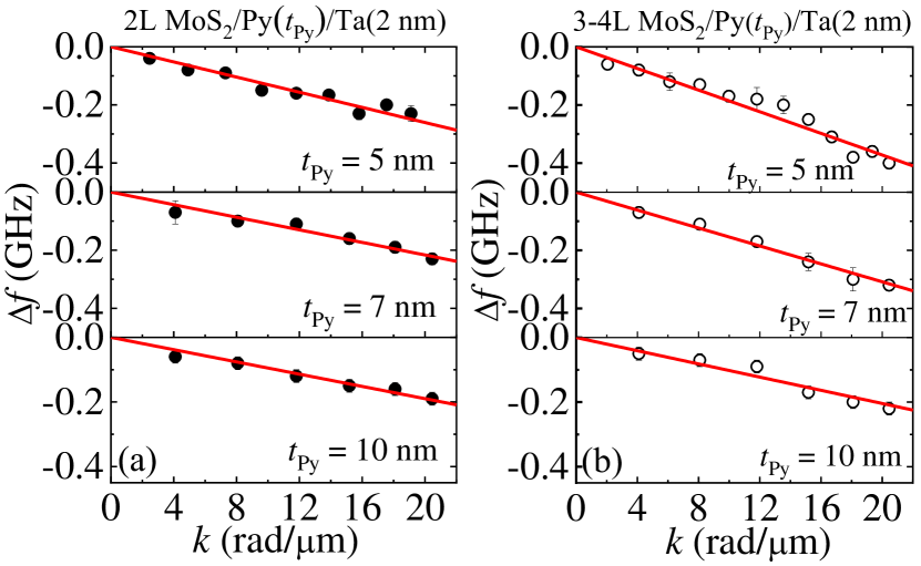
where, (=1.85 GHz/T) is the gyromagnetic ratio for Py thin-films. is the saturation magnetization, which was determined from thickness dependent ferromagnetic resonance (FMR) data and magnetometry measurements. Bansal et al. (2019) Figure 3 (a) and (b) shows frequency difference measured at different values for samples with various Py thickness for both 2L and 3-4L MoS2, respectively. The maximum value of is found to be around 0.3 GHz for 2L-MoS2/Py (5 nm) sample and 0.4 GHz for 3-4L MoS2/Py (5 nm) sample. The is also found to increase with the decrease of FM thickness indicating the dominance of DMI induced frequency non-reciprocity as opposed to the interfacial out-of-plane anisotropy induced frequency non-reciprocity which should vary linearly Stashkevich et al. (2015) or quadratically Gladii et al. (2016) with the thickness of the FM layer.
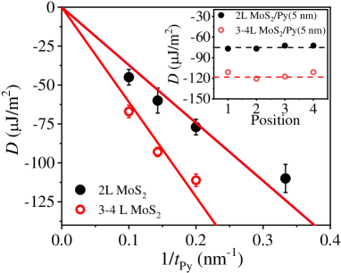
As the right hand side in Eq. (2) is linear with both and , the slope of the linear fit to vs. can be used to determine the DMI constant accurately. The data (black circles) in Fig. 3 was fitted (solid red line) using Eq. (2) to obtain the effective DMI constant. We can expect a linear behaviour of D with the inverse of FM layer thickness for the purely interfacial origin of DMI. Nembach et al. (2015); Belmeguenai et al. (2015); Chaurasiya et al. (2016) Figure 4 shows the measured value of as a function of inverse of Py thickness (1/) for both 2L (black solid circles) and 3-4L MoS2/Py (red open circles) samples. The solid lines in Fig. 4 shows linear fit to the data using the following equation: Belmeguenai et al. (2015)
| (3) |
Here, is the strength of the surface DMI parameter, which is independent of FM thickness. It is found that the pJ/m for 2L MoS2/Py and pJ/m for 3-4L MoS2/Py. The observed values are larger than the previously reported results on monolayer Graphene (=0.19 pJ/m) Chaurasiya et al. (2019) and are comparable to widely studied Pt heavy metal-based system ( pJ/m). Belmeguenai et al. (2015); Nembach et al. (2015) This sizable DMI value shows that MoS2 can be a very important material for spintronic and magnonic applications.
We also measure spatial variation of DMI in our 2L and 3-4L MoS2/Py bilayers, since we use large area MoS2. Inset of Fig. 4 shows the spatial dependence of D observed at different positions of the sample. The sample size was approximately 25 mm2 and the measurements are performed at the center and three other corners of the sample with approximate separation of mm. The laser spot width was about 50 m; hence these measurement positions are not overlapped with each other but significantly apart. The value of D for both 2L and 3-4L MoS2/Py does not show significant spatial variation with respect to the various positions of the samples as revealed by BLS measurement. The maximum variation is around 8.5 % for 3-4L MoS2/Py and 6.1 % for 2L MoS2/Py. Hence, higher DMI observed for in 3-4L MoS2/Py compared to 2L MoS2/Py is valid in the entire large area of the sample.
We found a larger for both 2L and 3-4L MoS2/Py samples compared to Graphene/Py, Chaurasiya et al. (2019) which can be attributed to larger spin-orbit coupling (SOC) of MoS2. Furthermore, the value of for 3-4L MoS2/Py sample is found significantly higher (56) than the 2L MoS2/Py. However, this result is counter-intuitive due to the following reason. The strength of DMI in FM/non-magnet system scales with SOC strength of the non-magnetic material in contact with the FM. It is known that intrinsic SOC in MoS2, which acts as a non-magnetic layer in our study, decreases with an increase in the number of layers. Chang et al. (2014) Hence, we expect a larger SOC in 2L MoS2 than 3-4L MoS2, as observed in our photo-luminescence measurements (not shown), which showed smaller spin splitting for 3-4L MoS2. Bansal et al. (2019) Hence, intrinsic SOC cannot explain the observed results. However, our earlier XPS data Barvat et al. (2017) and Raman mapping Bansal et al. (2019) on these MoS2 samples show the presence of higher sulfur vacancies in 3-4L MoS2 layer. In the XPS data, it is also observed that the presence of sulfur vacancies was primarily due to the formation of MoO3 species in the case of 3-4L MoS2. The large number of MoO3 species in the case of 3-4L MoS2 may be caused by the decomposition of MoS2 target for a higher number of laser shots used during PLD growth, which will increase the number of sulfur vacancies and promote the formation of MoO3 species. As previously shown that larger electronegativity leads to larger DMI. Torrejon et al. (2014) Since oxygen has a higher electronegativity of 3.44, compared to sulfur for which the electronegativity is 2.58. Hence, we argue that higher value of D observed in 3-4L MoS2/Py interface is due to the formation of local defects of MoO3. In BLS measurement, we measure volume averaged DMI constant, which can enhance due to the higher number of MoO3 defect species in the case of 3-4L MoS2/Py.
In conclusion, we have shown a direct measurement of sizable DMI constant for 2L and 3-4L MoS2/Py system using BLS measurements. The FM thickness dependence of DMI reveals the dominating interfacial origin of DMI in the studied system. We have observed a larger interfacial DMI in 3-4L MoS2/Py system as compared to 2L MoS2/Py, which can be correlated with the higher density of MoO3 defect species at the interface for 3-4L MoS2/Py. The maximum value of DMI constant obtained is comparable to that of previously reported values for Pt-based FM/HM heterostructures for the similar thickness of the FM layer. Hence, these results show the possibility of stabilizing chiral spin textures and their manipulation using already emerging unconventional spin-orbit torques in the 2D materials/FM system. Further, the iDMI at MoS2/Py interface can be controlled by engineering defects, which opens another pathway for the development of spintronic devices using 2D-TMDs.
The data that supports the findings of this study are available within the article.
Acknowledgements.
The partial support from the Ministry of Human Resource Development under the IMPRINT program (Grant no: 7519 and 7058), the Department of Electronics and Information Technology (DeitY), and Science and Engineering Research Board (SERB) under the Core Research Grant (CRG) (grant no: SERB/F/12383/2018-2019) are gratefully acknowledged. A. B. acknowledges S. N. Bose National Centre for Basic Sciences for financial assistance under grant no. SNB/AB/18-19/211. A. K. acknowledges support from the Council of Scientific and Industrial Research (CSIR), India, while A.K.C. acknowledges DST, Government of India for INSPIRE fellowship (Grant No. IF150922).References
- Dzialoshinskii (1957) I. E. Dzialoshinskii, JETP Lett. 32, 1547 (1957).
- Moriya (1960) T. Moriya, Phys. Rev. 120, 91 (1960).
- Roessler, Bogdanov, and Pfleiderer (2006) U. K. Roessler, A. Bogdanov, and C. Pfleiderer, Nature 442, 797 (2006).
- Bode et al. (2007) M. Bode, M. Heide, K. Von Bergmann, P. Ferriani, S. Heinze, G. Bihlmayer, A. Kubetzka, O. Pietzsch, S. Blügel, and R. Wiesendanger, Nature 447, 190 (2007).
- Parkin, Hayashi, and Thomas (2008) S. S. Parkin, M. Hayashi, and L. Thomas, Science 320, 190 (2008).
- Parkin and Yang (2015) S. S. Parkin and S.-H. Yang, Nat. Nano. 10, 195 (2015).
- Tomasello et al. (2014) R. Tomasello, E. Martinez, R. Zivieri, L. Torres, M. Carpentieri, and G. Finocchio, Sci. Rep. 4, 6784 (2014).
- Mühlbauer et al. (2009) S. Mühlbauer, B. Binz, F. Jonietz, C. Pfleiderer, A. Rosch, A. Neubauer, R. Georgii, and P. Böni, Science 323, 915 (2009).
- Yu et al. (2011) X. Yu, N. Kanazawa, Y. Onose, K. Kimoto, W. Zhang, S. Ishiwata, Y. Matsui, and Y. Tokura, Nat. Mater. 10, 106 (2011).
- Fert and Levy (1980) A. Fert and P. M. Levy, Phys. Rev. Lett. 44, 1538 (1980).
- Yang et al. (2015) H. Yang, A. Thiaville, S. Rohart, A. Fert, and M. Chshiev, Phys. Rev. Lett. 115, 267210 (2015).
- Husain et al. (2019) S. Husain, N. Sisodia, A. K. Chaurasiya, A. Kumar, J. P. Singh, B. S. Yadav, S. Akansel, K. H. Chae, A. Barman, P. Muduli, and S. Chaudhary, Sci. Rep. 9, 1085 (2019).
- Jiang et al. (2017) W. Jiang, G. Chen, K. Liu, J. Zang, S. G. Te Velthuis, and A. Hoffmann, Phys. Rep. 704, 1 (2017).
- Nembach et al. (2015) H. T. Nembach, J. M. Shaw, M. Weiler, E. Jué, and T. J. Silva, Nat. Phys. 11, 825 (2015).
- Di et al. (2015a) K. Di, V. L. Zhang, H. S. Lim, S. C. Ng, M. H. Kuok, X. Qiu, and H. Yang, Appl. Phys. Lett. 106, 052403 (2015a).
- Di et al. (2015b) K. Di, V. L. Zhang, H. S. Lim, S. C. Ng, M. H. Kuok, J. Yu, J. Yoon, X. Qiu, and H. Yang, Phys. Rev. Lett. 114, 047201 (2015b).
- Belmeguenai et al. (2015) M. Belmeguenai, J.-P. Adam, Y. Roussigné, S. Eimer, T. Devolder, J.-V. Kim, S. M. Cherif, A. Stashkevich, and A. Thiaville, Phys. Rev. B 91, 180405 (2015).
- Stashkevich et al. (2015) A. A. Stashkevich, M. Belmeguenai, Y. Roussigné, S. M. Cherif, M. Kostylev, M. Gabor, D. Lacour, C. Tiusan, and M. Hehn, Phys. Rev. B 91, 214409 (2015).
- Torrejon et al. (2014) J. Torrejon, J. Kim, J. Sinha, S. Mitani, M. Hayashi, M. Yamanouchi, and H. Ohno, Nat. Comm. 5, 4655 (2014).
- Baćani et al. (2019) M. Baćani, M. A. Marioni, J. Schwenk, and H. J. Hug, Sci. Rep. 9, 3114 (2019).
- Han (2016) W. Han, APL Mater. 4, 032401 (2016).
- Chaurasiya et al. (2016) A. K. Chaurasiya, C. Banerjee, S. Pan, S. Sahoo, S. Choudhury, J. Sinha, and A. Barman, Sci. Rep. 6, 32592 (2016).
- Chaurasiya et al. (2018) A. K. Chaurasiya, S. Choudhury, J. Sinha, and A. Barman, Phys. Rev. Appl. 9, 014008 (2018).
- Belmeguenai et al. (2016) M. Belmeguenai, M. S. Gabor, Y. Roussigné, A. Stashkevich, S. M. Chérif, F. Zighem, and C. Tiusan, Phys. Rev. B 93, 174407 (2016).
- Davydenko et al. (2019) A. V. Davydenko, A. G. Kozlov, A. G. Kolesnikov, M. E. Stebliy, G. S. Suslin, Y. E. Vekovshinin, A. V. Sadovnikov, and S. A. Nikitov, Phys. Rev. B 99, 014433 (2019).
- Raju et al. (2019) M. Raju, A. Yagil, A. Soumyanarayanan, A. K. Tan, A. Almoalem, F. Ma, O. Auslaender, and C. Panagopoulos, Nat. Comm. 10, 696 (2019).
- Chaurasiya et al. (2019) A. K. Chaurasiya, A. Kumar, R. Gupta, S. Chaudhary, P. K. Muduli, and A. Barman, Phys. Rev. B 99, 035402 (2019).
- Yang et al. (2018) H. Yang, G. Chen, A. A. Cotta, A. T. N’Diaye, S. A. Nikolaev, E. A. Soares, W. A. Macedo, K. Liu, A. K. Schmid, A. Fert, and M. Chshiev, Nat. Mater. 17, 605 (2018).
- Ajejas et al. (2018) F. Ajejas, A. Gudín, R. Guerrero, A. Anadón Barcelona, J. M. Diez, L. de Melo Costa, P. Olleros, M. A. Niño, S. Pizzini, J. Vogel, M. Valvidares, P. Gargiani, M. Cabero, M. Varela, J. Camarero, R. Miranda, and P. Perna, Nano Lett. 18, 5364 (2018).
- Xiao et al. (2012) D. Xiao, G.-B. Liu, W. Feng, X. Xu, and W. Yao, Phys. Rev. Lett. 108, 196802 (2012).
- MacNeill et al. (2017) D. MacNeill, G. M. Stiehl, M. H. D. Guimaraes, R. A. Buhrman, J. Park, and D. C. Ralph, Nat. Phys. 13, 300 (2017).
- Shao et al. (2016) Q. Shao, G. Yu, Y.-W. Lan, Y. Shi, M.-Y. Li, C. Zheng, X. Zhu, L.-J. Li, P. K. Amiri, and K. L. Wang, Nano lett. 16, 7514 (2016).
- Guimaraes et al. (2018) M. H. Guimaraes, G. M. Stiehl, D. MacNeill, N. D. Reynolds, and D. C. Ralph, Nano lett. 18, 1311 (2018).
- Zhu, Cheng, and Schwingenschlögl (2011) Z. Y. Zhu, Y. C. Cheng, and U. Schwingenschlögl, Phys. Rev. B 84, 153402 (2011).
- Barvat et al. (2017) A. Barvat, N. Prakash, B. Satpati, S. S. Singha, G. Kumar, D. K. Singh, A. Dogra, S. P. Khanna, A. Singha, and P. Pal, J. Appl. Phys. 122, 015304 (2017).
- Li et al. (2012) H. Li, Q. Zhang, C. C. R. Yap, B. K. Tay, T. H. T. Edwin, A. Olivier, and D. Baillargeat, Adv. Funct. Mater. 22, 1385 (2012).
- Mignuzzi et al. (2015) S. Mignuzzi, A. J. Pollard, N. Bonini, B. Brennan, I. S. Gilmore, M. A. Pimenta, D. Richards, and D. Roy, Phys. Rev. B 91, 195411 (2015).
- Bansal et al. (2019) R. Bansal, A. Kumar, N. Chowdhury, N. Sisodia, A. Barvat, A. Dogra, P. Pal, and P. Muduli, J. Magn. Magn. Mater. 476, 337 (2019).
- Gladii et al. (2016) O. Gladii, M. Haidar, Y. Henry, M. Kostylev, and M. Bailleul, Phys. Rev. B 93, 054430 (2016).
- Chang et al. (2014) T.-R. Chang, H. Lin, H.-T. Jeng, and A. Bansil, Sci. Rep. 4, 6270 (2014).