Local control of improper ferroelectric domains in YMnO3
Abstract
Improper ferroelectrics are described by two order parameters: a primary one, driving a transition to long-range distortive, magnetic or otherwise non-electric order, and the electric polarization, which is induced by the primary order parameter as a secondary, complementary effect. Using low-temperature scanning probe microscopy, we show that improper ferroelectric domains in YMnO3 can be locally switched by electric field poling. However, subsequent temperature changes restore the as-grown domain structure as determined by the primary lattice distortion. The backswitching is explained by uncompensated bound charges occuring at the newly written domain walls due to the lack of mobile screening charges at low temperature. Thus, the polarization of improper ferroelectrics is in many ways subject to the same electrostatics as in their proper counterparts, yet complemented by additional functionalities arising from the primary order parameter. Tailoring the complex interplay between primary order parameter, polarization, and electrostatics is therefore likely to result in novel functionalities specific to improper ferroelectrics.
I Introduction
In improper ferroelectrics, the spontaneous polarization emerges as subordinate effect to a primary order parameter which can be a lattice distortion, a magnetization or another non-electric quantity Levanyuk and Sannikov (1974); Kimura et al. (2003); Aken et al. (2004); Ikeda et al. (2005). This dependence can lead to properties not observed in their polarization-driven proper ferroelectric counterparts. Improper ferroelectrics can be expected to be more robust towards extrinsic influences, for example depolarizing fields, allowing domain configurations with unusual head-to-head or tail-to-tail polarization geometries at the domain walls Choi et al. (2010); Jungk et al. (2010). Such domain configurations can have technologically highly relevant properties, ranging from local conductance enhancementMeier et al. (2012); Oh et al. (2015); McQuaid et al. (2017) to functionalities of advanced circuit elementsMundy et al. (2017); Schaab et al. (2018).
Both order parameters of improper ferroelectrics, the primary one and the induced polarization, can in principle influence the domain structure, but while it appears obvious that the primary order parameter sets the initial domain structure when crossing the transition temperature, the role played by the secondary order parameter and the associated electrostatics is not as clear. In the case of the hexagonal manganites (MnO3, with = Sc, Y, In, Dy – Lu), one of the most established classes of improper ferroelectrics, a lattice-trimerizing distortion as primary order parameter dominates the formation of domains, but only the secondary order parameter is susceptible to controlled poling in an electric fieldLilienblum et al. (2015). Therefore, a key question is if, and how, domains associated with the primary order parameter formed at the transition temperature may differ from those created by electric field poling of the secondary order parameter within the ordered phase far below . Even though a detailed understanding of this complex interrelation is crucial for the functionalization of improper ferroelectrics, this aspect has not received much attention.
Here, we investigate electric-field poling at the nanometer scale in hexagonal YMnO3. In this material, uniform tilting of the MnO5 bipyramids in the unit cell and a concomitant shift of the ytttrium ions occur at . This lattice-trimerizing distortive transition drives an improper ferroelectric polarization of along the -axis Fiebig et al. (2002); Lottermoser et al. (2002); Kimura et al. (2003); Fennie and Rabe (2005); Jungk et al. (2010). The resulting domain structure consists of six trimerization-polarization domain states forming vortex-like meeting points with alternating polarization around the vortex coreChoi et al. (2010); Jungk et al. (2010); Meier et al. (2017).
We use atomic force microscopy (AFM) to apply local electric fields at cryogenic temperatures, where non-intrinsic effects due to barrier layer capacitances are negligibleRuff et al. (2017, 2018), creating polarization domains at the nanoscale. We compare these written domains to the domains formed via the primary order parameter at . We find that despite the secondary nature of the electric polarization, this polarization dominates the poling behavior just as in conventional ferroelectrics. Domains can be created at will by locally applied electric-fields. However, thermal annealing cycles return the samples to the as-grown domain configuration. This recovery is explained by uncompensated bound charges at the domain walls and the surface, which arise due to decreasing availability of mobile carriers in the semiconductor at low temperature. Hence, despite the secondary nature of the ferroelectric order, the electrostatic conditions overrule the primary lattice trimerization. Quite strikingly, we thus find that improper ferroelectrics retain key characteristics of proper ferroelectrics, yet complemented by functionalities introduced by the secondary nature of the electric order.
II Methods
Experiments were performed on YMnO3 single crystals grown by the floating-zone method Meier et al. (2017); Roessli et al. (2005). The crystals were cut into platelets with a thickness of approximately perpendicular to the crystallographic -axis. They were lapped with an Al2O3 solution and polished with silica slurry, yielding a surface roughness of approximately , suitable for AFM measurements. We thus obtained out-of-plane-polarized samples whose trimerization-polarization domains at the surface are separated by nominally uncharged side-by-side domain wallsChoi et al. (2010); Jungk et al. (2010); Meier et al. (2012).
Dielectric measurements were performed using a Novocontrol Alpha analyser (at to ) and a TF2000 Aixacct system (hystersis loops, at ) in combination with a high-voltage booster for voltages up to . Measurements were conducted at in a closed-cycle refrigerator with samples in vacuum to avoid electrical discharge. The properties of semiconducting materials are often superimposed by extrinsic barrier layer contributionsLunkenheimer et al. (2009) which may affect polarization measurementsScott (2007); Loidl et al. (2008). For YMnO3, a temperature of and a frequency of avoid barrier layer capacitances and allow detecting the genuine ferroelectric properties of the material both in bulk and AFM experimentsRuff et al. (2017, 2018).
AFM measurements were performed at in an attoLiquid 2000 AFM setup (attocube GmbH, Germany) with ANSCM-PT Pt/Ir-coated conductive tips (AppNano Inc., USA) in two different modes:
On the one hand, we directly imaged the distribution of the polarization by piezoresponse force microscopy (PFM)Kalinin and Gruverman (2007); Soergel (2011); Gruverman et al. (2019). In this mode, the AFM tip is brought into contact with the sample surface and an AC voltage is applied to the tip. The AFM detects the contraction and expansion of the sample due to the piezoelectric effect. A contraction in phase or in antiphase with the excitation voltage corresponds to polarization in the upward or downward direction, respectively.
On the other hand, we used the presence of uncompensated charges on the surface to image the domain structure by electrostatic force microscopy (EFM) Kalinin and Bonnell (2001); Schoenherr et al. (2019). Due to a difference in strength of the pyroelectric effect, the surface charge differs between domains and domain walls, which is detected as contrast in EFM measurements. For details of the EFM measurement procedure and temperature sequences, see Supplementary Information.
Local domain switching was achieved at by applying DC bias voltages to the AFM tip in contact with the sample surface.
III Results
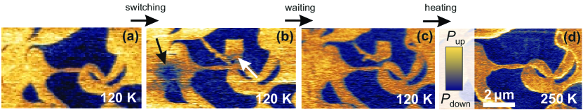
PFM measurements at showed the typical trimerization-induced improper ferroelectric domain structure of the hexagonal manganites (Fig. 1 a)). We then created a new domain by applying a voltage of + to the AFM tip while scanning a window of (Fig. 1 b)). This resulted in a square-shaped domain of upwards polarization within a down-polarized domain (white arrow). The black arrow points to a region where the same poling procedure was applied to an area which was already polarized upwards. The latter led to the injection of surface charges, visible as a diffuse dark region. At , the written domain was stable over a period of more than six days, whereas the space charges disappeared within a few hours (Fig. 1 c)). Finally, we found that when the sample was heated to , the domain structure reverted to its original configuration, i.e., the electric-field-induced square domain disappeared (Fig 1 d)).
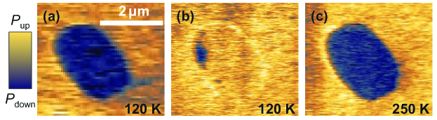
In order to investigate how the ferroelectric domain structure reverts to its previous configuration, we recorded a series of PFM images at higher spatial resolution. Figure 2 a) shows a down-polarized bubble domain within an up-polarized environment. After scanning a window of covering the entire bubble with + applied to the tip, the polarization was mostly reversed so that the bubble disappeared. A faint outline, however, was still observable where the previous as-grown domain wall had been located (Fig. 2 b)). This outline was possibly caused by the presence of oxygen interstitials, which are known to accumulate at neutral wallsSchaab et al. (2018), but are immobile at low temperatureRemsen and Dabrowski (2011) and hence cannot follow the displacement of the domain wall. When the sample was heated to , the original domain structure was recovered as depicted in Fig. 2 c).
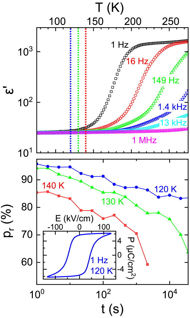
Complementary to the local measurements, we performed bulk dielectric spectroscopy and ferroelectric hystersis loop measurements to characterize the retention of the YMnO3 polarization and test for signatures of back-switching at the macro-scale. Measurements of the dielectric constant shown in Fig. 3 a) revealed a step-like increase of with temperature, indicating an intrinsic dielectric constant masked by barrier layer capacitance effectsLunkenheimer et al. (2002, 2009). Therefore, we chose our measurement temperature such that we could probe the intrinsic ferroelectric polarizationLunkenheimer et al. (2009); Ruff et al. (2017, 2018) (left of the dashed lines in Fig. 3 a)). Specifically, we performed all experiments at temperatures at or below 140 K. For confirmation, we measured a ferroelectric hysteresis loop at with an electrical poling field oscillating at (inset of Fig. 3 b). The shape of the loop and the saturation polarization are in perfect agreement with theoryFennie and Rabe (2005) and values of previous experiments Ruff et al. (2018); Han et al. (2013); Choi et al. (2010); Lilienblum et al. (2015), confirming that only the true polarization was measured.
To measure the retention behavior, first a pre-poling pulse with an applied electric field of was used to saturate the sample polarization. After a delay time ranging from to , positive-up-negative-down (PUND) measurements with the first pulse in the same electrical-field direction as the pre-poling pulse and a peak electric field of were performed to determine the remaining fraction of the saturated polarization , where denotes the initial polarization created by the pre-poling pulse and the measured polarization after the delay time . Figure 3 b) shows as a function of the delay time measured at three different temperatures. The equilibrium state towards which the system relaxes corresponds to , i.e., equal amount of up- and down polarized regions. At , the polarization reverted quickly to this equilibrium state after poling, whereas the value of polarization surplus was retained for several days at . These results are consistent with the reversal of polarization upon heating observed by the local switching experiments in Figs. 1 and 2.
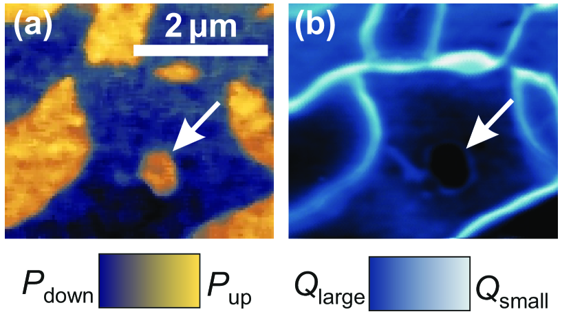
The domain walls of as-grown and electric-field-induced polar domains also showed different behavior when observed in EFM measurements. Because the overall conductivity is very low at , the domain wall conductance can not directly be measured by conductive AFM. However, EFM allows to image the electrostatics of domain walls even under insulating conditions (see Ref. Schoenherr et al., 2019 and Supplementary Information for details). Fig. 4 a) shows a PFM scan of the sample surface where a bubble domain was created by poling at (arrow). Here, in contrast to the measurements in which the AFM tip was scanned over a defined area with an applied voltage, the tip was stationary on the sample surface while applying the writing voltage. This resulted in the creation of a domain of about diameter as shown in Fig. 4 a).
The as-grown and the electric-field-induced domains exhibited the same brightness in PFM. Figure 4 b) shows an EFM image of the same area, measured at after the sample had been heated to . This temperature sequence creates an EFM contrast due to the pyroelectric effect associated with the temperature change, but preserves the written domain pattern because the temperature is not high enough for fast relaxation (see Supplementary Information for details). A pronounced EFM contrast was observed at as-grown domain walls, which is consistent with their enhanced conductivity attributed to the presence of oxygen interstitialsSchaab et al. (2018). At the domain walls associated with the written domains, however, the EFM contrast was substantially weaker, suggesting lower electronic conductance and, hence, a lower density of oxygen defects compared to the as-grown walls.
IV Discussion
We now discuss why electric-field-induced domains tend to return to their as-grown, trimerization-controlled configuration upon heating. First, we note that even though the electric-field poling acts on the polarization, the trimerization has to follow this reorientation because of the rigid coupling between secondary and primary order parameterKumagai and Spaldin (2013). Thus, we can exclude that the observed backswitching is due to an unswitched residue of the trimerized state.
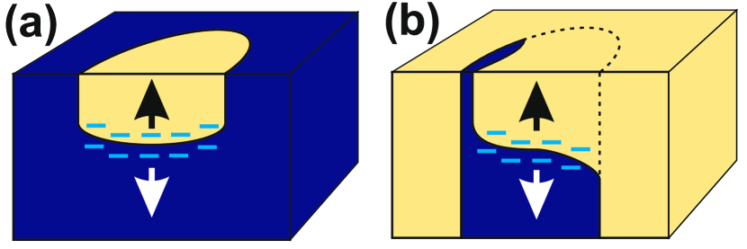
When the polarization at the sample surface is locally influenced by the AFM tip, it is affected only in a layer of a few hundreds of nanometers at the surface due to field-focusing below the AFM tip. Hence, the bulk polarization below the field-induced square domain in Fig. 1 remained unswitched. At the newly created domain wall below, the polarizations met tail-to-tail, resulting in uncompensated charges as is illustrated in Fig. 5 a). At elevated temperatures, such a configuration would be readily screened by charge carriers, but at the cryogenic temperature of our experiment, this screening process becomes extremely slow. Since the presence of uncompensated charges at the domain wall is energetically unfavorable, the material returned to its initial configuration when heated.
As-grown domains, on the other hand, exhibit no uncompensated charges and are therefore stable. An as-grown domain wall which had been erased by external electric fields was restored to its original shape by a temperature increase (Fig. 2). We conclude that defects, which show a propensity to accumulate at domain walls at high temperatures, but are immobilized at low temperaturesRemsen and Dabrowski (2011), could remain at their original location when a domain wall is displaced and serve as localized potential energy minima for the recovery of the domain structure. This hypothesis is corroborated by the remanent outline of the erased domain in Fig. 2 b) and the difference in domain-wall contrast between as-grown and electric-field-induced domain walls in Fig. 4 b), which can both be explained by a difference in defect density. Note that a similar dissociation of domain walls and defects during switching was previously found in BiFeO3 Stolichnov et al. (2014).
The intriguing consequence of these conclusions is that the electrostatic forces in the improper ferroelectric YMnO3 are strong enough to reverse not only the secondary, but also the primary order parameter, leading to the striking situation that the allegedly weaker secondary order parameter controls the stronger one.
Note that in all our local probe experiments, the topological protection of the domain structure by the primary order parameter did not play a role, because only bubbles, i.e., domains within existing domains, were created and erased, whereas the topological domain vortex meeting points were not affected. Therefore, we observed a behavior resembling that of proper ferroelectrics.
In our bulk switching experiments, on the other hand, the topological constraints imposed by the primary order parameter affected the poling behavior. Specifically, electric-field poling cannot destroy the topological domain vortices and therefore the sample cannot be transferred into a single-domain state Choi et al. (2010); Jungk et al. (2010). These unswitched remnants of the unfavored polarization direction then served as nuclei and memory in the relaxation of the polarization, a behavior not expected in proper ferroelectrics.
V Summary and Conclusions
We have shown that despite their origin in a non-polar, primary order parameter, the manipulation of polar domains in improper ferroelectric YMnO3 is guided by the same electrostatics as in proper ferroelectrics. In particular, the improper ferroelectric domain configuration can be manipulated by electric fields, and its dynamics upon heating is driven by charge accumulation. On the other hand, bulk measurements indicate that the topological protection of the domain configuration due to the primary order parameter prevents the sample from reaching the single-domain configuration of a proper ferroelectric, with consequences for the nucleation, pinning and conductance of the remaining ferroelectric domain walls. We thus conclude that with regard to external fields and charges, improper ferroelectrics behave like a proper ferroelectric in many respects, but the existence of the primary order parameter leads to intriguing additional functionalities.
VI Acknowledgments
The authors thank M. C. Weber for valuable help in sample preparation and A. Bortis, D. M. Evans and Q. N. Meier for helpful discussions. This research was supported by the EU European Research Council (Advanced Grant No. 694955—INSEETO) and the Swiss National Fund under grant numbers SNSF 20021_178825, 20021_149192 and 206021_150635. L.K. acknowledges support from an ETH Career Seed Grant. D.M. thanks NTNU for support through the Onsager Fellowship Program and the Outstanding Academic Fellows Program.
All authors discussed the results and contributed to the completion of the manuscript. L. K. and P. S. performed the low-temperature AFM experiments. S. K. and K. H. performed the dielectric spectroscopy measurements. E.P. grew the YMnO3 samples. S.K., T.L, M.T., D. M. and M.F. designed the experiment and supervised the study.
References
- Levanyuk and Sannikov (1974) A. P. Levanyuk and D. G. Sannikov, Soviet Physics Uspekhi 17, 199 (1974).
- Kimura et al. (2003) T. Kimura, T. Goto, H. Shintani, K. Ishizaka, T. Arima, and Y. Tokura, Nature 426, 55 (2003).
- Aken et al. (2004) B. B. V. Aken, T. T. Palstra, A. Filippetti, and N. A. Spaldin, Nature Materials 3, 164 (2004).
- Ikeda et al. (2005) N. Ikeda, H. Ohsumi, K. Ohwada, K. Ishii, T. Inami, K. Kakurai, Y. Murakami, K. Yoshii, S. Mori, Y. Horibe, and H. Kitô, Nature 436, 1136 (2005).
- Choi et al. (2010) T. Choi, Y. Horibe, H. T. Yi, Y. J. Choi, W. Wu, and S.-W. Cheong, Nature Materials 9, 253 (2010).
- Jungk et al. (2010) T. Jungk, Á. Hoffmann, M. Fiebig, and E. Soergel, Applied Physics Letters 97, 012904 (2010).
- Meier et al. (2012) D. Meier, J. Seidel, A. Cano, K. Delaney, Y. Kumagai, M. Mostovoy, N. A. Spaldin, R. Ramesh, and M. Fiebig, Nature Materials 11, 284 (2012).
- Oh et al. (2015) Y. S. Oh, X. Luo, F.-T. Huang, Y. Wang, and S.-W. Cheong, Nature Materials 14, 407 (2015).
- McQuaid et al. (2017) R. G. McQuaid, M. P. Campbell, R. W. Whatmore, A. Kumar, and J. M. Gregg, Nature Communications 8, 15105 (2017).
- Mundy et al. (2017) J. A. Mundy, J. Schaab, Y. Kumagai, A. Cano, M. Stengel, I. P. Krug, D. M. Gottlob, H. Doğanay, M. E. Holtz, R. Held, Z. Yan, E. Bourret, C. M. Schneider, D. G. Schlom, D. A. Muller, R. Ramesh, N. A. Spaldin, and D. Meier, Nature Materials 16, 622 (2017).
- Schaab et al. (2018) J. Schaab, S. H. Skjærvø, S. Krohns, X. Dai, M. E. Holtz, A. Cano, M. Lilienblum, Z. Yan, E. Bourret, D. A. Muller, M. Fiebig, S. M. Selbach, and D. Meier, Nature Nanotechnology 13, 1028 (2018).
- Lilienblum et al. (2015) M. Lilienblum, T. Lottermoser, S. Manz, S. M. Selbach, A. Cano, and M. Fiebig, Nature Physics 11, 1070 (2015).
- Fiebig et al. (2002) M. Fiebig, T. Lottermoser, D. Fröhlich, A. V. Goltsev, and R. V. Pisarev, Nature 419, 818 (2002).
- Lottermoser et al. (2002) T. Lottermoser, M. Fiebig, and D. Fröhlich, Journal of Applied Physics 91, 8251 (2002).
- Fennie and Rabe (2005) C. J. Fennie and K. M. Rabe, Physical Review B 72, 100103 (2005).
- Meier et al. (2017) Q. Meier, M. Lilienblum, S. Griffin, K. Conder, E. Pomjakushina, Z. Yan, E. Bourret, D. Meier, F. Lichtenberg, E. Salje, N. Spaldin, M. Fiebig, and A. Cano, Physical Review X 7, 041014 (2017).
- Ruff et al. (2017) E. Ruff, S. Krohns, M. Lilienblum, D. Meier, M. Fiebig, P. Lunkenheimer, and A. Loidl, Physical Review Letters 118, 036803 (2017).
- Ruff et al. (2018) A. Ruff, Z. Li, A. Loidl, J. Schaab, M. Fiebig, A. Cano, Z. Yan, E. Bourret, J. Glaum, D. Meier, and S. Krohns, Applied Physics Letters 112, 182908 (2018).
- Roessli et al. (2005) B. Roessli, S. N. Gvasaliya, E. Pomjakushina, and K. Conder, Journal of Experimental and Theoretical Physics Letters 81, 287 (2005).
- Lunkenheimer et al. (2009) P. Lunkenheimer, S. Krohns, S. Riegg, S. Ebbinghaus, A. Reller, and A. Loidl, The European Physical Journal Special Topics 180, 61 (2009).
- Scott (2007) J. F. Scott, Journal of Physics: Condensed Matter 20, 021001 (2007).
- Loidl et al. (2008) A. Loidl, S. Krohns, J. Hemberger, and P. Lunkenheimer, Journal of Physics: Condensed Matter 20, 191001 (2008).
- Kalinin and Gruverman (2007) S. Kalinin and A. Gruverman, eds., Scanning Probe Microscopy (Springer New York, 2007).
- Soergel (2011) E. Soergel, Journal of Physics D: Applied Physics 44, 464003 (2011).
- Gruverman et al. (2019) A. Gruverman, M. Alexe, and D. Meier, Nature Communications 10, 1661 (2019).
- Kalinin and Bonnell (2001) S. V. Kalinin and D. A. Bonnell, Physical Review B 63, 125411 (2001).
- Schoenherr et al. (2019) P. Schoenherr, K. Shapovalov, J. Schaab, Z. Yan, E. D. Bourret, M. Hentschel, M. Stengel, M. Fiebig, A. Cano, and D. Meier, Nano Letters 19, 1659 (2019).
- Remsen and Dabrowski (2011) S. Remsen and B. Dabrowski, Chemistry of Materials 23, 3818 (2011).
- Lunkenheimer et al. (2002) P. Lunkenheimer, V. Bobnar, A. V. Pronin, A. I. Ritus, A. A. Volkov, and A. Loidl, Physical Review B 66, 052105 (2002).
- Han et al. (2013) M.-G. Han, Y. Zhu, L. Wu, T. Aoki, V. Volkov, X. Wang, S. C. Chae, Y. S. Oh, and S.-W. Cheong, Advanced Materials 25, 2415 (2013).
- Kumagai and Spaldin (2013) Y. Kumagai and N. A. Spaldin, Nature Communications 4, 1540 (2013).
- Stolichnov et al. (2014) I. Stolichnov, M. Iwanowska, E. Colla, B. Ziegler, I. Gaponenko, P. Paruch, M. Huijben, G. Rijnders, and N. Setter, Applied Physics Letters 104, 132902 (2014).