DRAMDig: A Knowledge-assisted Tool to Uncover DRAM Address Mapping
Abstract
As recently emerged rowhammer exploits require undocumented DRAM address mapping, we propose a generic knowledge-assisted tool, DRAMDig, which takes domain knowledge into consideration to efficiently and deterministically uncover the DRAM address mappings on any Intel-based machines. We test DRAMDig on a number of machines with different combinations of DRAM chips and microarchitectures ranging from Intel Sandy Bridge to Coffee Lake. Comparing to previous works, DRAMDig deterministically reverse-engineered DRAM address mappings on all the test machines with only 7.8 minutes on average. Based on the uncovered mappings, we perform double-sided rowhammer tests and the results show that DRAMDig induced significantly more bit flips than previous works, justifying the correctness of the uncovered DRAM address mappings.
Index Terms:
Rowhammer, Reverse-engineer, DRAM Address Mapping, Knowledge-assisted Tool.I Introduction
DRAM is the main memory unit of modern computer systems and organized into rows. In 2014, Kim et al. [6] reported a software-induced DRAM fault, the so-called “rowhammer”, that is, intensive accessing two DRAM rows can cause bit flips in an adjacent row even without accessing the row. The fault was soon after exploited in cross memory boundary such as user-kernel [13] and VM-hypervisor [14]. To demonstrate a rowhammer exploit successfully, understanding how physical addresses are mapped to DRAM is a necessity [13, 10, 14] to efficiently and effectively induce rowhammer bit flips.
Although such mapping is available in AMD’s architectural manual but not published by another major chip company, Intel. As shown in Table I, Seaborn et al. [13] was the first to uncover the mapping. They first perform a blind rowhammer test, results of which are used to analyze DRAM address mapping of a specific machine. Although their methodology is intuitive and simple, the blind test is quite inefficient (within hours) and needs to be performed again if the machine setting changes (e.g., its microarchitecture or DRAM chips are replaced). To address the efficiency issue, Xiao et al. [14] applied a timing channel [9] to efficiently uncover DRAM address mapping. However, their tool only works in a limited number of machine settings (we actually experimented the code they shared and details are in Section IV-A). DRAMA [10] was the first to present a generic reverse-engineering tool that can be used in any Intel machines. It proposes a brute-force approach to enumerate all possible combinations of physical address bits and verify each combination based on the aforementioned timing channel. Due to its blind selection of physical addresses, DRAMA is inefficient (within hours) and often fails to output a deterministic DRAM address mapping (we tested their code 111https://github.com/IAIK/drama and details are in Section IV).
| Uncovering Tool | Generic | Efficient | Deterministic |
|---|---|---|---|
| Seaborn et al. [13] | (within hours) | ||
| Xiao et al. [14] | (within minutes) | ||
| DRAMA [10] | (within hours) | ||
| DRAMDig | (within minutes) |
Our contributions: In this paper, we revisit the limitations and advantages of the aforementioned algorithms and observe that none of them made full use of domain knowledge. With this key observation, we propose a generic knowledge-assisted tool, which utilizes domain knowledge (see Section III-A) to produce a deterministic DRAM address mapping on different machines. First, DRAMDig detects physical-address bits that index rows and columns, respectively. Second, the tool resolves the mappings from remaining bits to banks including channels, DIMMs, and ranks. Third, DRAMDig determines the bank bits that are also row bits or column bits.
We test DRAMDig on 9 different machine settings and it is able to efficiently and deterministically uncover the DRAM address mapping on each setting within only 7.8 minutes on average. Based on the uncovered mappings, we perform double-sided rowhammer tests on three different machine settings and all results show that DRAMDig is much more effective in inducing rowhammer bit flips than the other generic tool, DRAMA [10]. To this end, DRAMDig enables users to test how vulnerable their computers are to the rowhammer problem and also help evaluate the impact of existing rowhammer attacks [14, 2, 10, 4, 1] and rowhammer DRAM PUFs [11, 15].
In summary, we make the following key contributions:
-
•
We present a generic knowledge-assisted tool to reverse-engineer DRAM address mappings on both DDR3 and DDR4 chips for different CPU microarchitectures.
-
•
Compared to existing works, our proposed algorithm makes full use of system DRAM information, which makes itself efficient in generating a deterministic DRAM address mapping.
-
•
We perform rowhammer tests based on DRAMDig and have induced a significantly higher number of bit flips than previous works, justifying the correctness of our uncovered DRAM address mappings.
II Background and Related Work
In this section, we first describe the modern DRAM organization and then briefly introduce the rowhammer vulnerability.
II-A Dynamic Random-Access Memory
Dynamic Random-Access Memory (DRAM) modules are produced in the form of Dual Inline Memory Module (DIMM). A DIMM is directly connected to the CPU’s memory controller through one of two channels. A DIMM consists of one or two ranks, corresponding to its one or two sides. Each rank is further decomposed of multiple banks. A bank is structured as arrays of cells with rows and columns. When a memory access to a desired bank occurs, this “opens” a specified row by transferring all data in the row to the bank’s row buffer and a specified column from the row buffer will be accessed. As such, subsequent access to the same row will be served by the row buffer, while opening another row will flush the row buffer.
DRAM Refresh: The charge in the DRAM cell is not persistent and will drain over time due to various charge leakage reasons [6]. To prevent data loss, a periodic re-charge or refresh is required for all cells. DRAM specification specifies that the DRAM refresh interval is typically 32 or 64 ms, during which all cells within a rank will be refreshed.
DRAM Address Mapping: The CPU’s memory controller decides how physical-address bits are mapped to a DRAM address. A DRAM address refers to a 3-tuple of bank, row, column (DIMM, channel, and rank are included into the bank tuple). As this mapping is not publicly documented on a major processor platform, i.e., Intel, Seaborn et al. [12] observed that only different rows within the same bank can induce rowhammer bit flips. Based on this observation, they made an educated guess on the DRAM address mapping of an Intel Sandy Bridge CPU. Both DRAMA [10] and Xiao et al. [14] relied on a timing channel [9] to uncover the mapping.
II-B The Rowhammer Vulnerability
DRAM rows are vulnerable to persistent charge leakage induced by adjacent rows. Specifically, frequently opening (also known as rowhammer) one row within the DRAM refresh interval can cause bit flips to the neighboring rows. To trigger expected rowhammer bit flips from a modern CPU, an adversary has to clear the CPU caches and the row buffer, and gain the knowledge of how DRAM is accessed by the CPU. Firstly, all-level CPU cache must be flushed in order to hammer rows and this can be done explicitly by an unprivileged instruction (e.g., clflush) on x86 or implicitly by eviction sets of physical memory lines [1, 5, 3]. Secondly, bypassing the row buffer is also a necessity. Intuitively, hammering (i.e., frequently accessing) two different rows within the same bank in an alternate manner can bypass the row buffer. If two rows happen to be one row apart, such technique is called double-sided rowhammer. If not, then it is called single-sided rowhammer. Alternatively, one-location rowhammer [4] forces the memory controller to clear the row buffer and thus only needs to hammer one row. Lastly, to map a virtual address to a DRAM address, Memory Management Unit (MMU) will translate the virtual address to a physical address, which is mapped to a DRAM address by the memory controller. The virtual to physical mapping can be addressed by either accessing pagemap or forcing hugepage allocation. Clearly, a correct DRAM address mapping helps induce more rowhammer bit flips and thus affects existing rowhammer attacks [14, 2, 10, 4, 1] and rowhammer DRAM PUFs [11] as well as its attack [15].
III Overview
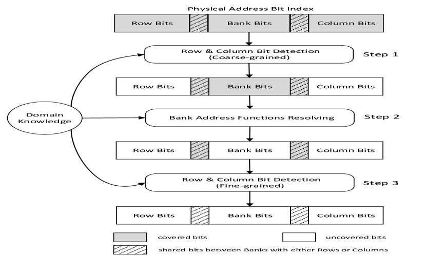
In this section, we describe a knowledge-assisted approach, named DRAMDig, to reverse engineer DRAM address mappings. As shown in Figure 1, DRAMDig consists of three main steps. In Step 1, we perform row and column bits detection and produce a coarse-grained results; that is, most row and column bits are uncovered while bits in grey boxes are still covered. In Step 2, we carefully select physical addresses that only differ in bits shown in grey boxes, then partition those addresses into different piles (addresses in each pile share the same bank), and identify bank address functions that can work for all piles. In Step 3, we perform a fine-grained analysis on the resolved bank address functions to detect row or column bits that also play a role in the bank address functions as shared bits (see lined boxes in Figure 1). Note that each step needs assistance from specific domain knowledge.
In the following sections, we first introduce the domain knowledge and a timing primitive, and then discuss the major three steps of DRAMDig in details.
III-A Domain Knowledge
We categorize the domain knowledge into three groups.
- •
-
•
System Information. This includes the total number of banks, physical memory size, and whether DRAM chips support ECC protection. This information can be obtained from the output of system commands such as decode-dimms and dmidecode.
-
•
Empirical observations. We have considered two aspects. Firstly, a bank address function on Intel microarchitecture is a tuple of multiple physical address bits, which are XORed to output a single bit. Secondly, since Ivy Bridge, the lowest bit of a bank address function that owns the most number of bits is not the column bit.
III-B A Timing Primitive
We resort to a timing channel [9] to reverse-engineer the DRAM mappings. Specifically, this timing channel is caused by the row-buffer conflicts within the same DRAM bank. As mentioned in Section II, each bank has a row buffer that caches the last accessed row. If a pair of addresses reside in two different rows of the bank and they are accessed alternately, the row buffer will be repeatedly reloaded and cleared. This causes the so-called row-buffer conflicts. Clearly, row buffer conflicts can lead to higher latency in accessing the two addresses than the case that they lie either within the same row or in different banks. As such, we can distinguish whether two addresses are in different rows within the same bank.
III-C Row & Column Bit Detection (Coarse-Grained)
We firstly partition the physical address bits into row, column and bank bits at a coarse-grained level. We use the same approach as the work [14]. Specifically, for row bits, we measure access latency for two physical addresses that only with one bit different. If the latency is high, that means those addresses reside within the same bank but different row (SBDR), and that bit is the only different bit for the two addresses, so it is a row bit.
For column bits, we select two physical addresses with only two bits being different, one being any detected row bit and the other being one non-row bit. If we get high latency for those two addresses, the non-row bit is a column bit. This because the two addresses are in the same bank, so neither of those bits is a bank bit, and then that non-row bit is a column bit that determine which column a physical address is mapped to. Finally, We consider the bits left are bank bits.
Note that the bits detection results in this step are coarse-grained. The row and column bits detected so far are only responsible for addressing rows and columns. There could be other row bits or column bits that also take responsibility for addressing banks, and they are not detected in this step. We will discuss how to identify them in section III-E.
III-D Bank Address Function Resolving
We uncover the bank address functions based on the above coarse-grained detection results. It consists of three phases. First, we calculate a number of specific address ranges based on the bank bits, and then select physical addresses within those ranges. Second, we partition the selected addresses into #bank number of piles, of which #bank can be known from the System Information in Section III-A. At last, we investigate those address piles and detect the bank address functions. We discuss the three phases in detail as follows.
Physical-Address Selection: The main idea is to only select the physical addresses within specific ranges. Such ranges reflect all possible values of all bank bits, so the selected addresses contain all the bank address functions. Besides, as the number of bank bits is determined through coarse-grained detection, the number of selected addresses can be determined. Algorithm 1 presents how we conduct physical-address selection.
The algorithm first calculates a , which indicates bank bits positions, and selects the physical pages that cover that range. (line 7-15). We don’t want miss any bank bits and thus we require that the selected physical pages are consecutive, and if there are some pages missed in , we try again. The last found physical page range is presented by .
Note that we use and to calculate range mask, but not all the bits in will be used in the bank address functions. We use “” to represent those bits that have nothing to do with the address functions such that we set the bits to 1. Next, for every investigated address with , we make it first mask against and then check whether the new address is valid and if so, we add it to , which holds final selected addresses. With “”, it enables us to only focus on the reasonable number of addresses that actually matter the address functions.
Physical Addresses Partition: We apply Algorithm 2 to partition the selected addresses into #bank numbers of piles.
First, we randomly select one address from and measure the latency with every other address. If the latency is high, it means we have one address that is SBDR with . We put it into which stores addresses from that are SBDR with (line 4-9). By doing so, we can collect all addresses from that are SBDR with and record them in . Next we verify whether the number of addresses in is within a valid range. If so, we consider this round of partition is successful, and then remove all the addresses in from and conduct next round of partition (line 10-12). Finally, it stops when enough addresses have been partitioned (line 13-15).
Ideally, all the addresses in will be partitioned into #bank number of piles with each pile having the same number of addresses. However, in practice the partition may be influenced by noises introduced by incorrect results of latency measurement, so it is possible that not all of piles have the same number of addresses, and also there may be some addresses that not partitioned into any pile. That’s why we introduce and and they can be adjusted in practice. Empirically, we set to 0.2 and to 85% and then the addresses can be successfully partitioned into #bank number of piles.
Bank Address Function Detection: We utilize Algorithm 3 to present how to detect bank address functions based on the address piles obtained.
| Machine | Microarch. | DRAM | Bank Address Functions | Row Bits | Column Bits | |
|---|---|---|---|---|---|---|
| No. | Type, Size | Config. | ||||
| No.1 | Sandy Bridge | DDR3, 8GiB | 2, 1, 1, 8 | (6), (14, 17), (15, 18), (16, 19) | 1732 | 05, 713 |
| i5-2400 | ||||||
| No.2 | Ivy Bridge | DDR3, 8GiB | 2, 1, 2, 8 | (14, 18), (15, 19), (16, 20), (17, 21), (7, 8, 9, 12, 13, 18, 19 ) | 1832 | 06, 813 |
| i5-3230M | ||||||
| No.3 | Ivy Bridge | DDR3, 4GiB | 1, 1, 2, 8 | (13, 17), (14, 18), (15, 19), (16, 20) | 1731 | 012 |
| i5-3230M | ||||||
| No.4 | Haswell | DDR3, 4GiB | 1, 1, 1, 8 | (13, 16), (14, 17), (15, 18) | 1631 | 012 |
| i5-4210U | ||||||
| No.5 | Haswell | DDR3, 16GiB | 2, 1, 2, 8 | (14, 18), (15, 19), (16, 20), (17, 21), (7, 8, 9, 12, 13, 18, 19 ) | 1832 | 06, 813 |
| i7-4790 | ||||||
| No.6 | Skylake | DDR4, 16GiB | 2, 1, 2, 16 | (7, 14), (15, 19), (16, 20), (17, 21), (18, 22), (8, 9, 12, 13, 18, 19) | 1933 | 07, 913 |
| i5-6600 | ||||||
| No.7 | Skylake | DDR4, 4GiB | 1, 1, 1, 8 | (6, 13), (14, 16), (15, 17) | 1631 | 012 |
| i5-6200U | ||||||
| No.8 | Coffee Lake | DDR4, 8GiB | 1, 1, 1, 16 | (6 13), (14 17), (15 18), (16, 19) | 1732 | 012 |
| i5-9400 | ||||||
| No.9 | Coffe Lake | DDR4, 16GiB | 2, 1, 2, 16 | (7, 14), (15, 19), (16, 20), (17, 21), (18, 22), (8, 9, 12, 13, 18, 19) | 1933 | 07, 913 |
| i5-9400 | ||||||
According to Empirical Observation in Section III-A, bank address functions take some bank bits as input and output values from those bank bits. Since we have grouped #bank number of piles and the addresses in each pile map to the same bank, we look into each pile and try all combinations of bank bits and apply each of them to the addresses in the pile. We look into the combination starting from one bit to the number of bank bits (line 1). If a combination of bank bits has the same XORed result for all the addresses in the pile, we consider it as a possible bank address function. After investigating all the piles, we can have all possible bank address functions (line 3-11).
However, some address functions are just linear combinations of the others so they are not the actual address functions and need to be removed. We consider the functions that have fewer bits have higher priority and remove the lower one if it is the linear combinations of higher priority functions. For instance, if (14, 18), (15, 19) and (14, 15, 18, 19) are 3 bank address functions. We consider the previous two have higher priority than the third, because the third is the linear combination of the previous two and we consider it as redundant (line 12-13).
Apart from that, the number of bank address functions should be . There may be more than that number of functions after removing the redundant, and they are not actual address functions. So we test every combination of number of functions and consider them as bank address functions, and use them to number the address piles. The actual bank address functions should be able to count those piles from to (line 14).
III-E Row & Column Bit Detection (Fine-Grained)
As discussed in section III-C, we need to determine the row bits and column bits that are also bank bits. From the Specifications in Section III-A, we can know the exact number of row and column bits for a specific DRAM chip, and since we have detected some row bits and column bits, we are able to determine how many row bits and column bits left to be uncovered.
For the remaining covered row bits, we start to investigate the bank address functions that consist of two bits. We select two physical address with only those two bits different and measure their latency. The two addresses actually map to the same bank. If the latency is actually high, it means either one bit is a row bit. We consider the higher one as the row bits as discussed in [12, 14]. If there are also row bits still covered after investigating two-bit address functions, we proceed to investigate address the bank functions that have more bits. In practice, we have not seen any case that needs to investigate the address functions that have three or more bits.
For the remaining covered column bits, we first check the number of remaining column bits that need uncovered, and then identify those bits that have not been identified as column bits in coarse-grained detection, denoted as . Next, according to the Empirical Observation in Section III-A, we know the lowest bit (denoted as ) of the function occupying the most number of bits is not a column bit. So we investigate the bits , by the order from low to high, and consider the first requested number of bits as column bits.
IV Evaluation
In this section, we first present DRAM address mappings uncovered by DRAMDig, and then evaluate its performance overhead. At last, we utilize the uncovered mappings on 3 machines to perform double-sided rowhammer tests.
IV-A Uncovered DRAM Address Mappings
We test DRAMDig on multiple Linux systems with different combinations of Intel microarchitectures and DRAM chips including DDR3 and DDR4. DRAMDig has successfully uncovered DRAM mappings including row and column bits and bank address functions for all the test settings, as shown in Table II. From the table, we see that DRAMDig has uncovered DRAM address mappings not only for mainstream CPU microarchitectures but also for a much newer CPU architecture (i.e., Coffee Lake) that previous works have never discussed.
Distinguish DRAMDig: When executing the code that Xiao el al. [14] shared with us, we found that it could not work on more than half of the machine settings, that is, No.2 and No.6-9. Take the No. 6 machine setting as an instance, the running code was stuck after resolving (16, 20), (17, 21), (18, 22) as 3 of 6 bank address functions. As such, their approach is not generic. For DRAMA [10], we ran their code for numerous times and found that it generated different DRAM mappings most of the time. As DRAMA is the first generic reverse-engineering tool, we further compare DRAMDig with it in terms of performance overhead and rowhammer tests in the following sections.
IV-B Performance Overhead
We present the performance overhead required by DRAMDig and DRAMA [10] respectively. As shown in Fig. 2, DRAMDig can be finished from 69 seconds to 17 minutes in all machines settings (only 7.8 minutes on average). In comparison, DRAMA spent from almost 500 seconds to 2 hours, indicating a much higher time cost than DRAMDig. Particularly in No.3 and No.7 settings, it cost roughly two hours without producing any results before we killed it.
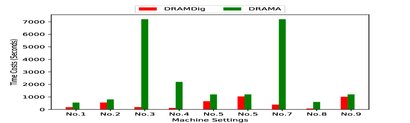
For DRAMDig, most of the time cost comes from the physical address partition, which is heavily affected by the number of selected physical addresses. The more selected addresses require more access latency measurements and thus the partition costs more time. Specifically, DRAMDig in No.6 and No.9 settings selected the highest number of physical addresses (almost 16,000), making itself timing-consuming. In contrast, it selected the least number (about 4000) in No.8 setting, thus making itself time-saving.
IV-C Rowhammer Tests
A correct DRAM address mapping is critical in effectively inducing rowhammer bit flips and thus can justify the correctness of uncovered DRAM address mappings. Since both Seaborn’s [13] and Xiao’s [14] tools are not generic and limited to one or multiple machine settings, we compare our work with another generic tool, DRAMA [10].
Specifically, we conducted double-sided rowhammer tests using the DRAM address mappings uncovered by DRAMDig and DRAMA respectively on three machine settings. For each setting, we performed 5 rowhammer tests and each lasted 5 minutes. The results are induced bit flips as shown in Table III. T1-T5 represent the 5 tests while the bit-flip numbers of each test are displayed in a way of DRAMDig/DRAMA. From the Total column, we can clearly see that DRAMDig caused significantly more bit flips than DRAMA while DRAMA even failed to induce any bit flips in some tests on No.2 and No.5. Also, the rowhammer test results justify the correctness of our uncovered DRAM address mappings.
| Machine | T1 | T2 | T3 | T4 | T5 | Total |
| No. | DRAMDig/DRAMA | |||||
| No.1 | 296/197 | 418/179 | 226/177 | 627/259 | 484/286 | 2051/1098 |
| No.2 | 959/240 | 934/0 | 976/18 | 1039/947 | 955/670 | 4863/1875 |
| No.5 | 12/7 | 12/0 | 12/0 | 10/0 | 11/0 | 57/7 |
V Conclusion
In this paper, we proposed a generic knowledge-assisted tool, DRAMDig, which applied domain knowledge to efficiently and deterministically reverse-engineer DRAM address mappings. We evaluated DRAMDig on a bunch of machines with different DRAM chips and CPU microarchitectures settings. The experiments showed that DRAMDig was able to deterministically uncover DRAM address mappings on all the test machines with only 69 seconds in the best case and 17 minutes in the worst case. We also performed double-sided rowhammer tests with our uncovered DRAM address mappings and made comparison with DRAMA, and the results indicated that DRAMDig could induce significantly more bit flips, which justified the correctness of our tool. As a result, we are going to open-source our tool to help users better understand DRAM address mapping and evaluate the impact of rowhammer attacks and rowhammer DRAM PUFs.
References
- [1] Z. B. Aweke, S. F. Yitbarek, R. Qiao, R. Das, M. Hicks, Y. Oren, and T. Austin. Anvil: Software-based protection against next-generation rowhammer attacks. ACM SIGPLAN Notices, 51(4):743–755, 2016.
- [2] Y. Cheng, Z. Zhang, S. Nepal, and Z. Wang. Cattmew: Defeating software-only physical kernel isolation. IEEE Transactions on Dependable and Secure Computing, 2019.
- [3] D. Genkin, L. Pachmanov, E. Tromer, and Y. Yarom. Drive-by key-extraction cache attacks from portable code. In International Conference on Applied Cryptography and Network Security, pages 83–102. Springer, 2018.
- [4] D. Gruss, M. Lipp, M. Schwarz, D. Genkin, J. Juffinger, S. O’Connell, W. Schoechl, and Y. Yarom. Another flip in the wall of rowhammer defenses. arXiv preprint arXiv:1710.00551, 2017.
- [5] D. Gruss, C. Maurice, and S. Mangard. Program for testing for the dram rowhammer problem using eviction. https://github.com/IAIK/rowhammerjs, May 2017.
- [6] Y. Kim, R. Daly, J. Kim, C. Fallin, J. H. Lee, D. Lee, C. Wilkerson, K. Lai, and O. Mutlu. Flipping bits in memory without accessing them: An experimental study of dram disturbance errors. In ACM SIGARCH Computer Architecture News, volume 42, pages 361–372. IEEE Press, 2014.
- [7] Micron, Inc. Ddr3 sdram mt41k2g4rkb, mt41k1g8trf, mt41k512m16vrn data sheet. https://www.micron.com/products/dram/ddr3-sdram/, 2015.
- [8] Micron, Inc. Ddr4 sdram mt40a2g4, mt40a1g8, mt40a512m16 data sheet. https://www.micron.com/products/dram/ddr4-sdram/, 2015.
- [9] T. Moscibroda and O. Mutlu. Memory performance attacks: Denial of memory service in multi-core systems. In USENIX Security Symposium, 2007.
- [10] P. Pessl, D. Gruss, C. Maurice, M. Schwarz, and S. Mangard. Drama: Exploiting dram addressing for cross-cpu attacks. In USENIX Security Symposium, pages 565–581, 2016.
- [11] A. Schaller, W. Xiong, N. A. Anagnostopoulos, M. U. Saleem, S. Gabmeyer, S. Katzenbeisser, and J. Szefer. Intrinsic rowhammer pufs: Leveraging the rowhammer effect for improved security. In 2017 IEEE International Symposium on Hardware Oriented Security and Trust (HOST), pages 1–7. IEEE, 2017.
- [12] M. Seaborn. How physical addresses map to rows and banks in dram. http://lackingrhoticity.blogspot.com.au/2015/05/how-physical-addresses-map-to-rows-and-banks.html.
- [13] M. Seaborn and T. Dullien. Exploiting the dram rowhammer bug to gain kernel privileges. In Black Hat’15.
- [14] Y. Xiao, X. Zhang, Y. Zhang, and R. Teodorescu. One bit flips, one cloud flops: Cross-vm row hammer attacks and privilege escalation. In USENIX Security Symposium, pages 19–35, 2016.
- [15] S. Zeitouni, D. Gens, and A.-R. Sadeghi. It’s hammer time: how to attack (rowhammer-based) dram-pufs. In Proceedings of the 55th Annual Design Automation Conference, page 65. ACM, 2018.