Flux-induced topological superconductivity in full-shell nanowires
Abstract
We present a novel route to realizing topological superconductivity using magnetic flux applied to a full superconducting shell surrounding a semiconducting nanowire core. In the destructive Little-Parks regime, reentrant regions of superconductivity are associated with integer number of phase windings in the shell. Tunneling into the core reveals a hard induced gap near zero applied flux, corresponding to zero phase winding, and a gapped region with a discrete zero-energy state around one applied flux quantum, , corresponding to phase winding. Theoretical analysis indicates that in the presence of radial spin-orbit coupling in the semiconductor, the winding of the superconducting phase can induce a transition to a topological phase supporting Majorana zero modes. Realistic modeling shows a topological phase persisting over a wide range of parameters, and reproduces experimental tunneling conductance data. Further measurements of Coulomb blockade peak spacing around one flux quantum in full-shell nanowire islands shows exponentially decreasing deviation from periodicity with device length, consistent with Majorana modes at the ends of the nanowire.
I Introduction
Majorana zero modes (MZMs) at the ends of one-dimensional topological superconductors are expected to exhibit non-trivial braiding statistics Read2000 ; Kitaev01 ; Alicea2011 , opening a path toward topologically protected quantum computing Nayak2008 ; DasSarma2015 . Among the proposals to realize MZMs, one approach Lutchyn2010 ; Oreg2010 based on semiconducting nanowires with strong spin-orbit coupling subject to a Zeeman field and superconducting proximity effect has received particular attention, yielding numerous compelling experimental signatures Mourik2012 ; Deng2016 ; Albrecht2016 ; Zhang2018 ; Lutchyn2018 . An alternative route to MZMs aims to create vortices in spinless superconductors, by various means, for instance by coupling a vortex in a conventional superconductor to a topological insulator Fu2008 ; Chiu11 ; Cook11 ; deJuan14 ; Xu2015 or conventional semiconductor Sau2010 ; Alicea2010 , using doped topological insulators Hosur2011 , iron-based superconductors Wang2018 , or using vortices in exotic quantum Hall analogs of spinless superconductors DasSarma2005 .
In this Article, we demonstrate both experimentally and theoretically that a hybrid nanowire consisting of a full superconducting (Al) shell surrounding a semiconducting (InAs) core can be driven into a topological phase that supports MZMs at the wire ends by a flux-induced winding of the superconducting phase. This conceptually new approach contains elements of both proximitized-wire schemes Lutchyn2010 ; Oreg2010 and vortex-based schemes Read2000 ; Fu2008 for creating MZMs. The topological phase sets in at relatively low magnetic fields, is controlled discretely by moving from zero to one phase twists around the superconducting shell, and does not require a large factor in the semiconductor, broadening the landscape of candidate materials.
While it is known that well-chosen superconducting phase differences can be used to break time-reversal symmetry and localize MZMs in semiconducting heterostructures Romito2012 ; vanHeck2014 ; Kotetes2015 ; Hell2017 ; Pientka2017 ; Stanescu2018 , the corresponding realizations typically require careful tuning of the fluxes. In contrast, vortices in a full-shell wire provide a naturally quantized means of controlling superconducting phase. In the destructive Little-Parks regime Little1962 ; deGennes1981 , the modulation of critical current and temperature with flux applied along the hybrid nanowire results in a sequence of lobes with reentrant superconductivity Liu2001 ; Sternfeld2011 . Each lobe is associated with a quantized number of twists of the superconducting phase Tinkham1966 , determined by the external field so that the free energy of the superconducting shell is minimized. The result is a series of topologically locked boundary conditions for the proximity effect in the semiconducting core, with a dramatic effect on the subgap density of states.
Our measurements reveal that tunneling into the core in the zeroth superconducting lobe, around zero flux, yields a hard proximity-induced gap with no subgap features. In the superconducting regions around one quantum of applied flux, corresponding to phase twists of in the shell, tunneling spectra into the core shows stable zero-bias peaks, indicating a discrete subgap state fixed at zero energy.
Theoretically, we find that a Rashba field arising from the breaking of local radial inversion symmetry at the semiconductor-superconductor interface Antipov2018 ; Mikkelsen2018 ; Woods2019 , along with -phase twists in the boundary condition, can induce a topological state supporting MZMs. We calculate the topological phase diagram of the system as a function of various parameters such as Rashba spin-orbit coupling, radius of the semiconducting core and band bending at the superconductor-semiconductor interface Antipov2018 ; Mikkelsen2018 ; Woods2019 . Our analysis shows that topological superconductivity extends in a reasonably large portion of the parameter space. Transport simulations of the tunneling conductance in the presence of Majorana zero modes qualitatively reproduce the experimental data in the entire voltage-bias range.
We obtain further experimental evidence that the zero-energy states are localized at wire ends by investigating Coulomb blockade conductance peaks in full-shell wire islands of various lengths. In the zeroth lobe, Coulomb blockade peaks show spacing, indicating Cooper-pair tunneling and an induced gap exceeding the island charging energy. In the first lobe, peak spacings are roughly -periodic, with slight even-odd alternation that vanishes exponentially with island length consistent with overlapping Majorana modes at the two ends of the Coulomb island, as investigated previously Albrecht2016 ; vanHeck2016 . The exponential dependence on length, and incompatibility with a power-law dependence, strongly suggests that MZMs reside at the ends of the hybrid islands.
II Device description
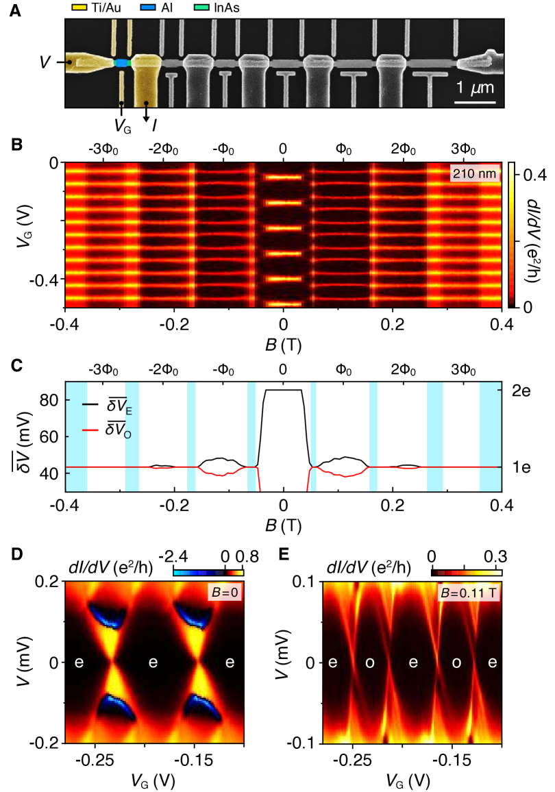
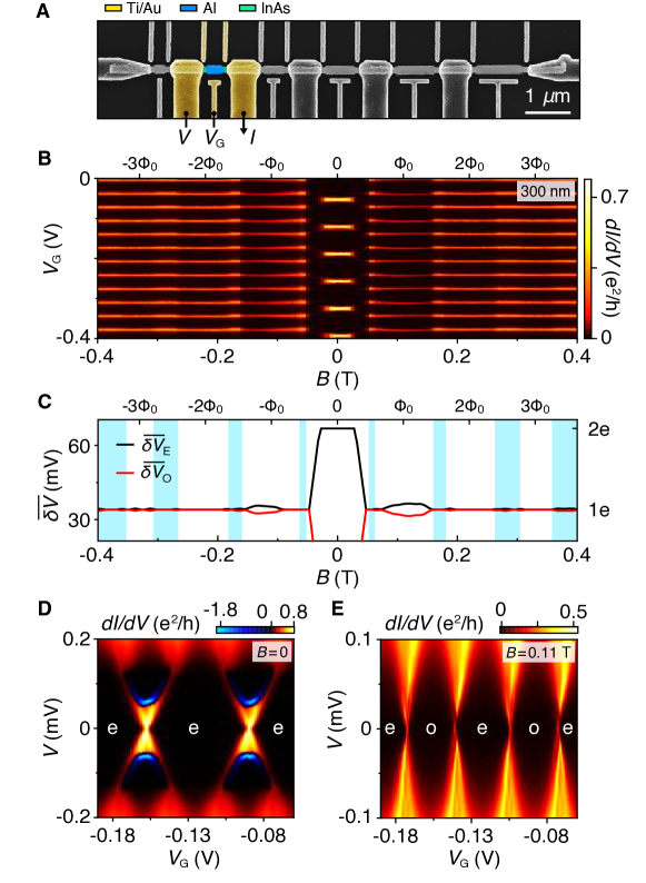
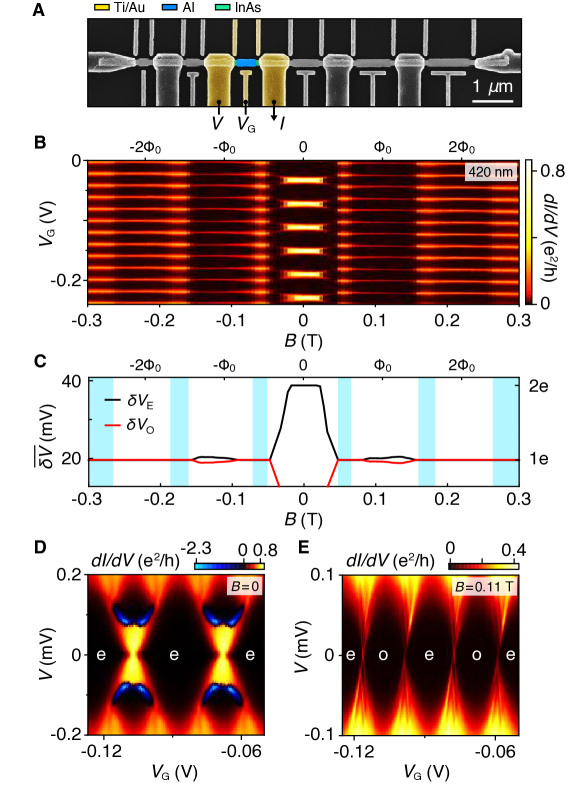
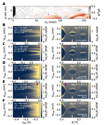
InAs nanowires were grown by the vapor-liquid-solid method using molecular beam epitaxy (MBE). The nanowires had a hexagonal cross section with maximum diameter nm. A 30 nm epitaxial Al layer was grown while rotating the sample, yielding a fully enclosing shell (Fig. 1A) Krogstrup2015 . Devices were fabricated using electron-beam lithography. Standard ac lock-in measurements were carried out in a dilution refrigerator with a base temperature of 20 mK. Magnetic field was applied parallel to the nanowire using three-axis vector magnet. Two device geometries, measured in three devices each, showed similar results. Data from two representative devices are reported in the main text: device 1 was used for 4-probe measurements of the shell (Fig. 1B) and tunneling spectroscopy of the core (Fig. 2A); device 2 comprised six Coulomb islands of different lengths fabricated on a single nanowire, each with separate ohmic contacts, two side gates to trim tunnel barriers, and a plunger gate to change occupancy (Fig. 6A). Supporting data from additional three tunneling devices, one of which has thinner shell, and two Coulomb-blockaded devices are presented in Supplementary . For more detailed description of the wire growth, device fabrication and measurement techniques see Supplementary .

Differential resistance of the shell, , measured for device 1 as a function of bias current, , and axial magnetic field, , showed a lobe pattern characteristic of the destructive regime (Fig. 1C) with maximum switching current of A at , the center of the zeroth lobe. Between the zeroth and first lobes, supercurrent vanished at mT, re-emerged at mT, and had a maximum near the center of the first lobe, at mT. A second lobe with smaller critical current was also observed, but no third lobe.
Temperature dependence of around zero bias yielded a reentrant phase diagram with superconducting regions separated by destructive regions with temperature-independent normal-state resistance (Fig. 1D). and shell dimensions from Fig. 1A yield a Drude mean free path of nm. The dirty-limit shell coherence length Tinkham1966 ; Gordon1984
| (1) |
can then be found using the zero-field critical temperature K from Fig. 1D and Fermi velocity of Al, m/s Kittel2005 , with Planck constant and Boltzmann constant , yielding nm. The same values for is found using the onset of the first destructive regime Schwiete2009 .
III Tunneling spectroscopy
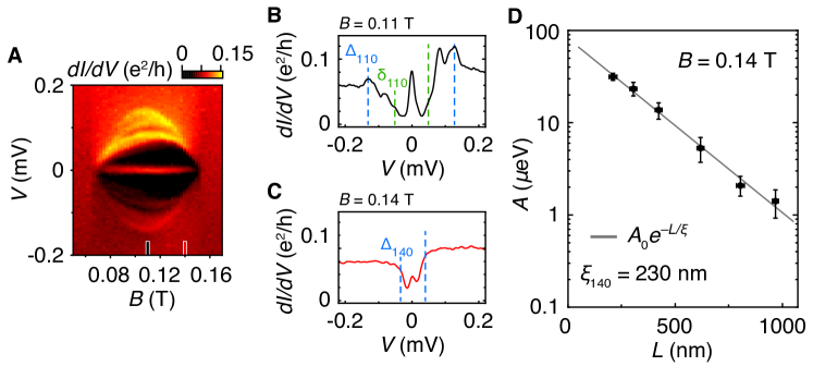
Differential conductance, , as a function of source-drain voltage, , measured in the tunneling regime as a probe of the local density of states at the end of the nanowire is shown in Fig. 2. The Al shell was removed at the end of the wire and the tunnel barrier was controlled by the global back-gate at voltage . At zero field, a hard superconducting gap was observed throughout the zeroth superconducting lobe (Fig. 2, B and D). Similar to the supercurrent measurements presented above, the superconducting gap in the core closed at mT and reopened at mT, separated by a gapless destructive regime. Upon reopening, a narrow zero-bias conductance peak was observed throughout the first gapped lobe (Fig. 2, B and F). Several flux-dependent subgap states are also visible, separated from the zero-bias peak in the first lobe. These nonzero subgap states are analogs of Caroli-de Gennes-Matricon bound states Caroli1964 , in this case confined at the metal-semiconductor interface rather than around a vortex core.
The first lobe persists to mT, above which a second gapless destructive regime was observed. A second gapped lobe centered around mT then appeared, containing several subgap states away from zero energy, as shown in greater detail in Supplementary . The second lobe closes at mT, above which only normal-state behavior was observed.
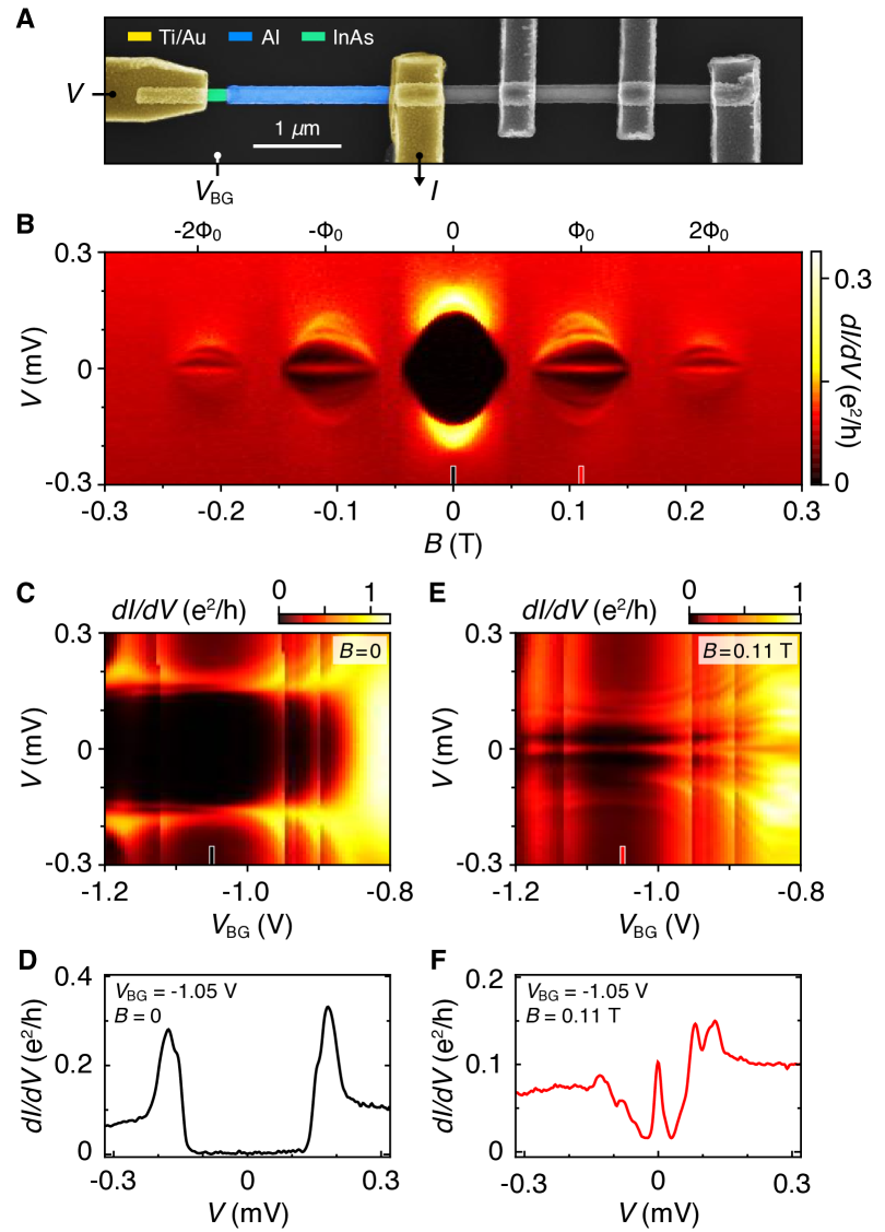
The dependence of tunneling spectra on back-gate voltage in the zeroth lobe is shown in Fig. 2C. In weak tunneling regime, for V a hard gap was observed, with eV (Fig. 2, C and D). As the device is opened, for V subgap conductance is enhanced due to Andreev processes. The increase in conductance at V is likely due to a resonance in the barrier. In the first lobe, at mT, the sweep of showed a zero-energy state throughout the tunneling regime (Fig. 2E). The cut displayed in Fig. 2F shows a discrete zero-bias peak well separated from other states. As the tunnel barrier is opened, the zero-bias peak gradually evolves into a zero-bias dip. This behavior is in qualitative agreement with theory Vuik2018 , although the crossover occurs at lower conductance than expected. Additional line-cuts as well as the tunneling spectroscopy for the second lobe are provided in Supplementary . Several switches in data occurred at the same gate voltages in Fig. 2, C and E, presumably due to gate-dependent charge motion in the barrier.
IV Modeling of topological phases
To better understand the origin of the zero-energy modes in the first lobe we analyze theoretically a semiconducting nanowire covered by a superconducting shell. First, we present a toy model of a cylindically symmetric full-shell wire (Fig. 3), highlighting the underlying mechanism of the topological phase appearance. Thereafter we move on to simulations of realistic geometries (Fig. 4 and Fig. 5).
We assume that the semiconductor (InAs) has a large Rashba spin-orbit coupling due to the local inversion symmetry breaking in the radial direction at the semiconductor-superconductor interface (corresponding to an electric field pointing along the radial direction at the superconductor-semiconductor interface). The system is subject to a magnetic field along the direction of the nanowire, . Using cylindrical coordinates and the symmetric gauge for the electromagnetic vector potential, , the effective Hamiltonian for the semiconducting core can be written as (henceforth )
| (2) |
Here is the electron momentum operator, the electric charge, the effective mass, is the chemical potential, the strength of the Rashba spin-orbit coupling, and finally are spin- Pauli matrices. , and are the cylindrical unit vectors. For ease of presentation, we consider -independent and in our model, which may be viewed as averaged versions of the corresponding -dependent quantities. The vector potential , where is the flux threading the cross-section at radius . For simplicity, we neglect the Zeeman term due to the small magnetic fields required in the experiment.
The superconducting shell (Al) induces superconducting correlations in the nanowire due to Andreev processes at the semiconductor-superconductor interface. If the tunnel coupling to the superconductor is weak, the induced pairing in the nanowire can be expressed as a local potential (see Ref. Supplementary ). In the Nambu basis , the Bogoliubov-de-Gennes (BdG) Hamiltonian for the proximitized nanowire is then given by
| (5) |
We assume that the thickness of the shell is smaller than London penetration depth: . Therefore, the magnetic flux threading the shell is not quantized. However, the magnetic field induces a winding of the superconducting phase of the order parameter with the angular coordinate and the winding number determined by the external magnetic flux.
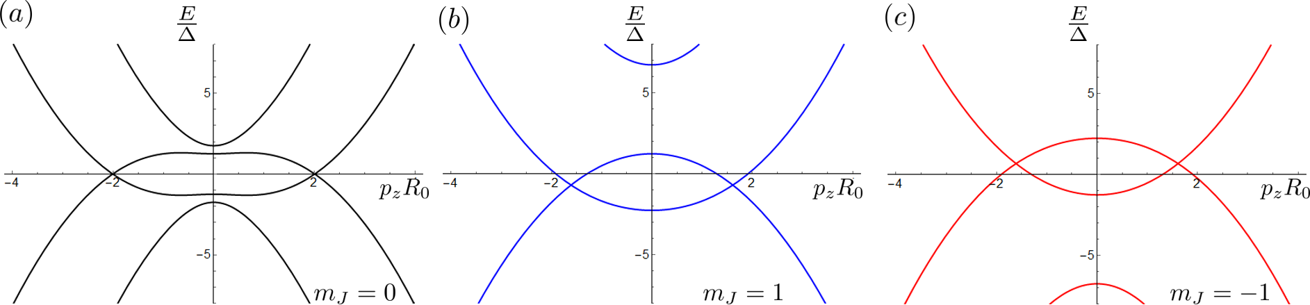
We notice the following rotational symmetry of the BdG Hamiltonian: with , where we introduced matrices acting in Nambu space. Eigenstates of can thus be labeled by a conserved quantum number : . The wave function has to be single-valued, which imposes the following constraint on :
| (6) |
It is interesting to note that the particle-hole symmetry relates states with opposite energy and angular quantum number , that is with , where represents complex conjugation. Thus, the sector—allowed when the winding number is odd—is special as it allows non-degenerate Majorana solutions at zero energy, as we show below.
The angular dependence of can be eliminated via a unitary transformation , namely where
| (7) | ||||
Here and . Note that naively one might expect spin-orbit coupling to average out; however, the non-trivial structure of -eigenvectors yields finite matrix elements proportional to the Rashba spin-orbit coupling.
Assuming that the electrons in the core are localized at the interface we set (Fig. 3A). This approximation is motivated by the fact that there is an accumulation layer in certain semiconductor-superconductor heterostructures such as InAs/Al, as explained below. In this case the electrons in semiconductor effectively form a thin-wall hollow cylinder and one can consider only the lowest-energy radial mode in Eq. (7). This allows for an analytical solution of the model. The effective Hamiltonian for the hollow-cylinder model reads
| (8) | ||||
Here, and the parameters and correspond to the effective chemical potential and Zeeman energy. and represent the coupling of the generalized angular momentum with magnetic field and electron spin, respectively. They are defined as
| (9) | ||||
| (10) | ||||
| (11) | ||||
| (12) |
with .
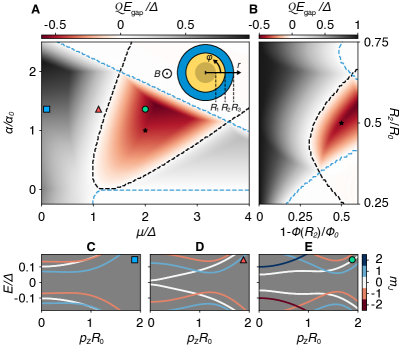
Equations (9)-(12) allow to identify a topological phase in the sector of the first lobe where . In this case, and , and one can map Eq. (25) to the Majorana nanowire model of Refs. Lutchyn2010 ; Oreg2010 . Notice that the effective Zeeman term has an orbital origin here and is present even when the factor in the semiconductor is zero. Both and can be tuned by the magnetic flux , which may induce a topological phase transition. In the hollow cylinder approximation when the core is penetrated by one flux quantum (). This regime corresponds to the trivial (s-wave) superconducting phase. However, a small deviation of the magnetic flux can drive the system into the topological superconducting phase FootnoteFlux . Indeed, the Zeeman and spin-orbit terms in Eq. (25) do not commute and thus opens a gap in the spectrum at . At the topological quantum phase transition between the two phases, the gap in the sector,
| (13) |
closes. The resulting phase diagram is shown in Fig. 3, where the gap closing at the topological transition is indicated by black dashed lines. Close to the transition, the quasiparticle spectrum in the sector is given by with and the corresponding topological coherence length .
A well-defined topological phase requires the quasiparticle bulk gap to be finite for all values of . Due to the angular symmetry of Eq. (25), different sectors do not mix and, as a result, the condition for a finite gap in the sectors is Supplementary . In general, the topological phase diagram can be obtained by calculating the topological index Kitaev01 ,
| (14) |
where and correspond to trivial and topological phases, respectively. Thus, the topological phase supporting MZMs appears due to the change of in the sector. In Fig. 3 we show the topological phase diagram and energy gap of the hollow cylinder model determined by taking into account all sectors.
The hollow cylinder model provides conceptual understanding for the existence of the topological phase in full shell nanowires. The model, however, is limited to small chemical potentials and a conserved angular momentum. For a direct comparison with the experiment more realistic simulations extending to the regime with multiple radial modes are needed.
V Realistic simulations
Recent advances in the modelling of semiconductor-superconductor hybrid structures have led to more accurate simulations of proximitized nanowires Vuik16 ; Mikkelsen2018 ; Antipov2018 ; Winkler2018 . Here, the essence of our approach is to integrate out the superconductor into self-energy boundary conditions, as discussed in Supplementary . This approximation allows for three-dimensional (3D) simulations of proximitized nanowires, including important effects such as self-consistent electrostatics and orbital magnetic field contribution Winkler17 .
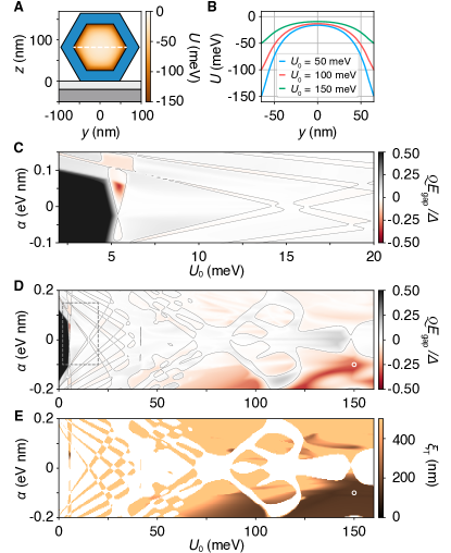
We model a hexagonal InAs wire with 130 nm corner-to-corner diameter coated by a 30 nm thick Al shell, see Fig. 4A. The work function difference between InAs and Al leads to a band offset between the conduction band of InAs and the Fermi level of Al resulting in an electron accumulation layer close to the interface, see Fig. 4, A and B. This band offset is on the order of 100 meV Antipov2018 ; Mikkelsen2018 ; Winkler2018 ; Schuwalow2019 . Due to the accumulation layer, there is an intrinsic electric field for the electrons, resulting in Rashba spin-orbit coupling with the symmetry axis in approximately radial direction Footnote1 ; Winkler2003 . The magnitude of has been experimentally determined to be in the range of 0.02 to 0.08 eV nm Lutchyn2018 .
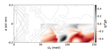
Given the uncertainties, we calculate the topological phase diagram as a function of band offset, , and the Rashba spin-orbit coupling, Wimmer2012 . The band offset controls the number of subbands in the nanowire as well as their population. For meV the system is in the single radial mode regime and the phase diagram appears qualitatively similar to the hollow-cylinder model, see Fig. 4, C and D. Around 5 meV there is a gapped topological phase which we identify with the angular sector, analog to the hollow-cylinder model. Specifically in this regime, apart from the sector, the topological phases have very small gap. The vertical feature at meV band offset in Fig. 4D corresponds to a second radial subband with crossing the Fermi level.
For meV the phase diagram becomes qualitatively different. Due to the increased number of bands the different topological phases hybridize and merge into extended topological regions Sticlet2017 ; LutchynFisher11 . Furthermore, as increases the wave functions are pushed closer to the superconductor leading to a stronger hybridization of the wave functions with Al. In this region one finds extended topological regions with sizable gaps which are a significant fraction of the superconducting gap.
Mixing of different angular sectors, facilitated by the broken cylindrical symmetry due to the hexagonal cross section, lifts the restriction of gapped topological phases to the sector. In this context, we note that when angular symmetry is broken (due to disorder in superconductor or geometrical effects) and is not a good quantum number, the topological superconducting phase may also appear at even winding numbers (see Supplementary for the topological phase diagram in the second lobe).
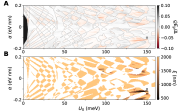
In addition to the gap size we also compute the topological coherence length, (Fig. 4E), from the eigenvalue decomposition of the translation operator at zero energy Nijholt16 . As expected, regions with large gap also have a short coherence length. Note that due to the smaller Fermi velocity in the semiconductor, the topological coherence length can be smaller than the s-wave coherence length. We find that the shortest nm, whereas the typical values for realistic spin-orbit coupling strength and band offset range between 140 and 200 nm.
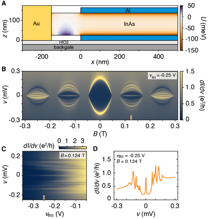
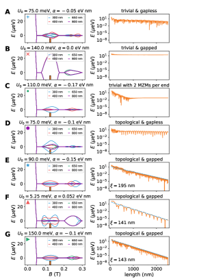
Having established bulk properties, we numerically compute a three-dimensional full shell wire in a transport geometry. The corresponding longitudinal cross section of the simulated device is shown in Fig. 5A. After calculating the electrostatic potential of the 3D structure we simulate the quantum transport using the package Kwant and adaptive kwant ; adaptive . In the main text we focus on a single point in the phase diagram with band offset of 150 meV and eV nm (see the white circle in Fig. 4, D and E). Results for other representative points can be found in Supplementary .
Computed conductance, , as a function of bias voltage, v, and magnetic field, , is shown in Fig. 5B. The simulated back-gate voltage, , is chosen such that there is good visibility of states in the wire. Similar to the experiment, the zeroth lobe shows a hard gap with no subgap states. The first and second lobes on the other hand show multiple subgap states FootnoteAsymmetry . The first lobe has a gap with a zero-bias peak due to Majorana end states. The size of the gap is consistent with the bulk phase diagram in Fig. 4D. The second lobe has more subgap states and appears to be gapless.
The evolution of the simulated spectrum with the back-gate voltage in the topological phase is displayed in Fig. 5C. As expected, the bias voltages at which zero-bias peak and subgap states are visible is independent of but the intensities of the states change. Since the wire is fully covered by a superconducting shell the effect of the back gate is completely screened inside the bulk of the wire and does not influence the topological phase or bulk states. When the junction becomes very open at V the zero-bias peak transforms into a zero-bias dip, as expected in this regime.
VI Coulomb blockade spectroscopy
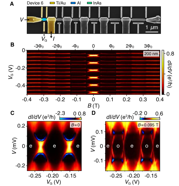
Returning to experiment, we next investigate MZM hybridization, which can be measured using the spacing of Coulomb blockade conductance peaks in Coulomb islands as a function of island length Albrecht2016 ; vanHeck2016 ; OFarell2018 ; Shen2018 . The exponential length dependence of hybridization energy is a signature of MZMs localized at the opposite ends of the nanowire Cheng2009 ; Fu2010 ; Chiu2017 . We investigated full-shell islands over a range of device lengths from nm to nm, fabricated on a single nanowire, as shown in Fig. 6.
Zero-bias conductance as a function of plunger-gate voltage, , and for device 2 yielded series of Coulomb blockade peaks for each segment, examples of which are shown in Fig. 6B. The corresponding average peak spacings, , for even and odd Coulomb valleys as a function of are shown in Fig. 6C. Around zero field, Coulomb-blockade peaks with periodicity were found. These peaks split at 40 mT toward the high-field end of the zeroth superconducting lobe, as the superconducting gap decreased below the charging energy of the island. The peaks then became -periodic (within experimental sensitivity) around mT and throughout the first destructive regime (see also Fig. 1 for the onset of destructive regime). When superconductivity reappeared in the first lobe, the Coulomb peaks did not become spaced by again, but instead showed nearly spacing with even-odd modulation. The nm island showed a qualitatively similar even-odd also in the second lobe. Unlike device 1 described in Fig. 2, the shortest island in device 2 also showed a third superconducting lobe, which can be identified from the peak height contrast in Fig. 6B. Coulomb blockade peaks were -periodic within experimental sensitivity throughout the third lobe.
Tunneling spectra at finite source-drain bias showed Coulomb diamonds around zero field (Fig. 6D) and nearly diamonds at mT, near the middle of the first lobe (Fig. 6E). The zero-field diamonds are indistinguishable from each other, showing a region of negative differential conductance associated with the onset of quasiparticle transport Hekking1993 ; Hergenrother1994 ; Higginbotham2015 . In the first lobe (Fig. 6E), Coulomb diamonds alternate in size and symmetry, with degeneracy points showing sharp, gapped structure, indicating that the near-zero-energy state is discrete. Additional resonances at finite bias reflect excited discrete subgap states away from zero energy.
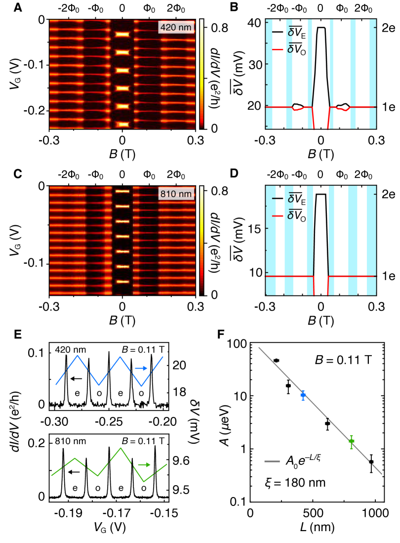
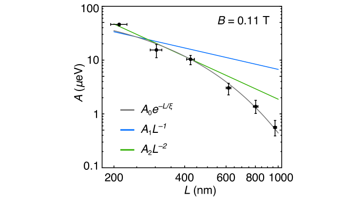
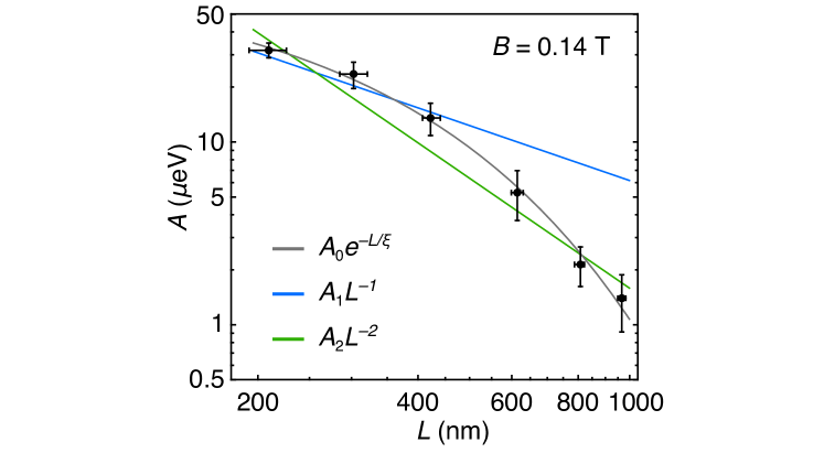
Coulomb peaks for two longer islands are shown in Fig. 7, A to E, with full data sets for other lengths reported in Supplementary . All islands showed -periodic Coulomb peaks in the zeroth lobe and nearly spacing in the first lobe. Examining the 420 nm and 810 nm data in Fig. 7, A, C and E already reveals that the mean difference between even and odd peak spacings in the first lobe decreased with increasing island length. To address this question quantitatively, we determine the lever arm, , for each island independently in order to convert plunger gate voltages to chemical potentials on the islands, using the slopes of the Coulomb diamonds Thijssen2008 ; Albrecht2016 . This allows the peak spacing differences (Fig. 7, B and D) to be converted to island-energy differences, , between even and odd occupations, as a function of device length, (a detailed exemplar peak spacing analysis is presented in Supplementary ). Within a Majorana picture, the energy scale reflects the length dependent hybridization energy of MZMs. Values for at mT, in the middle of the first lobe, spanning over two orders of magnitude are shown in Fig. 7F. A fit to an exponential yields fit parameters eV and nm. The data are well described by an exponential length dependence, implying that the low-energy modes are located at the ends of the wire, not bound to impurities or local potential fluctuations as expected for overlapping Majorana modes. The comparison of exponential and power-law fits as well as the calculated length dependence that shows exponential decay only in topological regimes are provided in Supplementary . The measured is consistent with the calculated using realistic parameters.
Along with length dependent even-odd peak spacing difference, we observe even-odd modulation in peak heights, see Fig. 7E. Possible explanation of these phenomena was proposed in Ref. Hansen2018 . Additionally, we find a complex alternating peak-height structure depending on magnetic field within the first lobe. Peak height modulation accompanying peak spacing modulation was observed previously Albrecht2016 ; OFarell2018 ; Shen2018 .
To investigate how coherence length , extracted from the exponential decrease of even-odd peak spacing with length, depends on the superconducting gap, , we examine peak spacing near the high-field edge of the first lobe, mT, where the gap is reduced to eV, and shows no subgap features besides the zero-bias peak Supplementary . At this reduced gap we again find an exponential dependence on length, and incompatibility with a power law, now with nm. We observe that is consistent with simple scaling, (not accounting for a field-dependent velocity). From Fig. 2B and Ref. Supplementary , eVeV , where is the lowest non-zero subgap state, and . We also note that both and are slightly smaller than the coherence length in the superconducting shell at corresponding B-field values: nm and nm, extracted from data in Fig. 1D using Eq. (1) and the corresponding values of . This discrepancy may be interpreted as resulting from the velocity renormalization in the semiconductor in the strong coupling limit Stanescu2011 ; nadj2013 ; Peng2015 .
VII Conclusions and Outlook
In this Article, we demonstrated experimentally and theoretically that threading magnetic flux through a semiconducting nanowire fully covered by a superconducting shell can induce a topological phase with Majorana zero modes at the nanowire ends. While being of similar simplicity and practical feasibility Krogstrup2015 as the original nanowire proposals with a partial shell coverage Lutchyn2010 ; Oreg2010 , full-shell nanowires provide several key advantages. First, the topological transition in a full-shell wire is driven by the field-induced winding of the superconducting order parameter, rather than by the Zeeman effect so that, as demonstrated in the reported measurements, the required magnetic fields can be very low ( T). Therefore, the present proposal is compatible with conventional superconducting electronics and removes the need for a large factor semiconductor, potentially expanding the landscape of candidate materials. Moreover, the full shell naturally protects the semiconductor from impurities and random surface doping, thus enabling a reproducible way of growing many wires with essentially identical electrostatic environments. Although full-shell wires do not allow for direct gating of the electron density in the semiconducting core, we demonstrated that via a careful design of the wire properties, for example by choosing the appropriate radius, it is possible to obtain wires that harbor MZMs at a predictable magnetic field. The modest magnetic field requirements, protection of the semiconducting core from surface defects, and locked phase winding in discrete lobes together suggest a new and relatively easy route to creating and controlling Majorana zero modes in hybrid materials. Our findings open a possibility to study an interplay of mesoscopic and topological physics in this novel system.
VIII Acknowledgments
We thank A. Antipov, L. Casparis, M. Freedman, A. Higginbotham, E. Martinez for valuable discussions, J. Gamble and J. Gukelberger for contributions to the simulation code, as well as C. Sørensen, R. Tanta and S. Upadhyay for contributions to material growth and device fabrication. Research was supported by Microsoft, the Danish National Research Foundation, and the European Commission. This work was performed in part at Aspen Center for Physics, which is supported by National Science Foundation grant PHY-1607611. M.T.D. acknowledges support from State Key Laboratory of High Performance Computing, China. L.I.G. acknowledges support from NSF DMR Grant No. 1603243.
References
- (1) N. Read, D. Green, Phys. Rev. B 61, 10267 (2000).
- (2) A. Y. Kitaev, Phys. Usp. 44, 131 (2001).
- (3) J. Alicea, Y. Oreg, G. Refael, F. von Oppen, M. P. A. Fisher, Nat. Phys. 7, 412 (2011).
- (4) C. Nayak, S. H. Simon, A. Stern, M. Freedman, S. Das Sarma, Rev. Mod. Phys. 80, 1083 (2008).
- (5) S. Das Sarma, M. Freedman, C. Nayak, NPJ Quant. Inf. 1, 15001 (2015).
- (6) R. M. Lutchyn, J. D. Sau, S. Das Sarma, Phys. Rev. Lett. 105, 077001 (2010).
- (7) Y. Oreg, G. Refael, F. von Oppen, Phys. Rev. Lett. 105, 177002 (2010).
- (8) V. Mourik, et al., Science 336, 1003 (2012).
- (9) M. T. Deng, et al., Science 354, 1557 (2016).
- (10) S. M. Albrecht, et al., Nature 531, 206 (2016).
- (11) H. Zhang, et al., Nature 556, 74 (2018).
- (12) R. M. Lutchyn, et al., Nat. Rev. Mater. 3, 52 (2018).
- (13) L. Fu, C. L. Kane, Phys. Rev. Lett. 100, 096407 (2008).
- (14) C.-K. Chiu, M. J. Gilbert, T. L. Hughes, Phys. Rev. B 84, 144507 (2011).
- (15) A. Cook, M. Franz, Phys. Rev. B 84, 201105 (2011).
- (16) F. de Juan, R. Ilan, J. H. Bardarson, Phys. Rev. Lett. 113, 107003 (2014).
- (17) J.-P. Xu, et al., Phys. Rev. Lett. 114, 017001 (2015).
- (18) J. D. Sau, R. M. Lutchyn, S. Tewari, S. Das Sarma, Phys. Rev. Lett. 104, 040502 (2010).
- (19) J. Alicea, Phys. Rev. B 81, 125318 (2010).
- (20) P. Hosur, P. Ghaemi, R. S. K. Mong, A. Vishwanath, Phys. Rev. Lett. 107, 097001 (2011).
- (21) D. Wang, et al., Science 362, 333 (2018).
- (22) S. Das Sarma, M. Freedman, C. Nayak, Phys. Rev. Lett. 94, 166802 (2005).
- (23) A. Romito, J. Alicea, G. Refael, F. von Oppen, Phys. Rev. B 85, 020502 (2012).
- (24) B. van Heck, S. Mi, A. R. Akhmerov, Phys. Rev. B 90, 155450 (2014).
- (25) P. Kotetes, Phys. Rev. B 92, 014514 (2015).
- (26) M. Hell, M. Leijnse, K. Flensberg, Phys. Rev. Lett. 118, 107701 (2017).
- (27) F. Pientka, et al., Phys. Rev. X 7, 021032 (2017).
- (28) T. D. Stanescu, A. Sitek, A. Manolescu, Beilstein J. Nanotechnol. 9, 1512 (2018).
- (29) W. A. Little, R. D. Parks, Phys. Rev. Lett. 9, 9 (1962).
- (30) P.-G. de Gennes, C. R. Acad. Sci. Paris 292, 279 (1981).
- (31) Y. Liu, et al., Science 294, 2332 (2001).
- (32) I. Sternfeld, et al., Phys. Rev. Lett. 107, 037001 (2011).
- (33) M. Tinkham, Introduction to Superconductivity (McGraw Hill, New York, ed. 2, 1996).
- (34) A. E. Antipov, et al., Phys. Rev. X 8, 031041 (2018).
- (35) A. E. G. Mikkelsen, P. Kotetes, P. Krogstrup, K. Flensberg, Phys. Rev. X 8, 031040 (2018).
- (36) B. D. Woods, S. Das Sarma, T. D. Stanescu, Phys. Rev. B 99, 161118 (2019).
- (37) B. van Heck, R. M. Lutchyn, L. I. Glazman, Phys. Rev. B 93, 235431 (2016).
- (38) P. Krogstrup, et al., Nat. Mater. 14, 400 (2015).
- (39) See Supplemental Material.
- (40) J. M. Gordon, C. J. Lobb, M. Tinkham, Phys. Rev. B 29, 5232 (1984).
- (41) C. Kittel, Introduction to Solid State Physics (Wiley, ed. 8, 2005).
- (42) G. Schwiete, Y. Oreg, Phys. Rev. Lett. 103, 037001 (2009).
- (43) C. Caroli, P. G. De Gennes, J. Matricon, Phys. Lett. 9, 307 (1964).
- (44) A. Vuik, B. Nijholt, A. R. Akhmerov, M. Wimmer, SciPost Phys. 7, 61 (2019).
- (45) Note that magnetic flux piercing the finite-thickness superconducting shell can be significantly different from that penetrating the core.
- (46) A. Vuik, D. Eeltink, A. R. Akhmerov, M. Wimmer, New J. Phys. 18, 033013 (2016).
- (47) G. W. Winkler, et al., Phys. Rev. B 99, 245408 (2019).
- (48) G. W. Winkler, et al., Phys. Rev. Lett. 119, 037701 (2017).
- (49) S. Schuwalow, et al., arXiv:1910.02735 (2019).
- (50) With our sign convention this electric field results in an of negative sign. However, there are also other contributions to from strain and microscopic details of the InAs-Al interface. The sign of the spin-orbit coupling is difficult to predict due to this.
- (51) R. Winkler, Spin-orbit coupling effects in two-dimensional electron and hole systems, Springer tracts in modern physics (Springer, Berlin, 2003).
- (52) M. Wimmer, ACM Trans. Math. Softw. 38, 30:1 (2012).
- (53) D. Sticlet, B. Nijholt, A. Akhmerov, Phys. Rev. B 95, 115421 (2017).
- (54) R. M. Lutchyn, M. P. A. Fisher, Phys. Rev. B 84, 214528 (2011).
- (55) B. Nijholt, A. R. Akhmerov, Phys. Rev. B 93, 235434 (2016).
- (56) C. W. Groth, M. Wimmer, A. R. Akhmerov, X. Waintal, New J. Phys. 16, 063065 (2014). The code is publicly available at https://kwant-project.org/.
- (57) B. Nijholt, J. Weston, J. Hoofwijk, A. Akhmerov, Adaptive: parallel active learning of mathematical functions (2019). The code is publicly available at https://github.com/python-adaptive/adaptive.
- (58) The asymmetry of the conductance of subgap states in bias voltage in our simulation is a consequence of a dissipation term eV Liu2017 .
- (59) E. C. T. O’Farrell, et al., Phys. Rev. Lett. 121, 256803 (2018).
- (60) J. Shen, et al., Nat. Commun. 9, 4801 (2018).
- (61) M. Cheng, R. M. Lutchyn, V. Galitski, S. Das Sarma, Phys. Rev. Lett. 103, 107001 (2009).
- (62) L. Fu, Phys. Rev. Lett. 104, 056402 (2010).
- (63) C.-K. Chiu, J. D. Sau, S. Das Sarma, Phys. Rev. B 96, 054504 (2017).
- (64) F. W. J. Hekking, L. I. Glazman, K. A. Matveev, R. I. Shekhter, Phys. Rev. Lett. 70, 4138 (1993).
- (65) J. M. Hergenrother, M. T. Tuominen, M. Tinkham, Phys. Rev. Lett. 72, 1742 (1994).
- (66) A. P. Higginbotham, et al., Nat. Phys. 11, 1017 (2015).
- (67) J. M. Thijssen, H. S. J. Van der Zant, Phys. Status Solidi B 245, 1455 (2008).
- (68) E. B. Hansen, J. Danon, K. Flensberg, Phys. Rev. B 97, 041411 (2018).
- (69) T. D. Stanescu, R. M. Lutchyn, S. Das Sarma, Phys. Rev. B 84, 144522 (2011).
- (70) S. Nadj-Perge, I. K. Drozdov, B. A. Bernevig, A. Yazdani, Phys. Rev. B 88, 020407 (2013).
- (71) Y. Peng, F. Pientka, L. I. Glazman, F. von Oppen, Phys. Rev. Lett. 114, 106801 (2015).
- (72) C.-X. Liu, J. D. Sau, T. D. Stanescu, S. Das Sarma, Phys. Rev. B 96, 075161 (2017).
- (73) T. O. Rosdahl, A. Vuik, M. Kjaergaard, A. R. Akhmerov, Phys. Rev. B 97, 045421 (2018).
- (74) QDevil ApS, http://www.qdevil.com.
- (75) I. Vurgaftman, J. R. Meyer, L. R. Ram-Mohan, Journal of Applied Physics 89, 5815 (2001).
- (76) N. Ashcroft, N. Mermin, Solid State Physics (Cengage Learning, 2011).
- (77) This approximation is well justified given the much larger effective mass of Al compared to InAs Rosdahl2018 .
- (78) T. Kiendl, F. von Oppen, P. W. Brouwer, Phys. Rev. B 100, 035426 (2019).
- (79) is measured from the center to a corner of an effective hexagon.
- (80) While the chosen in the simulation is slightly different from the experimentally measured nm, the gap-field dependence is still very close in simulation and experiment.
- (81) V. H. Dao, L. F. Chibotaru, Phys. Rev. B 79, 134524 (2009).
- (82) M. Lee, J. S. Lim, R. López, Phys. Rev. B 87, 241402 (2013).
- (83) Our results also apply to the case of and .
- (84) A. I. Larkin, Sov. Phys. JETP 21, 153 (1965).
- (85) N. C. Koshnick, H. Bluhm, M. E. Huber, K. A. Moler, Science 318, 1440 (2007).
- (86) C. Beenakker, Phys. Rev. B 44, 1646 (1991).
- (87) J. F. Cochran, D. E. Mapother, Phys. Rev. 111, 132 (1958).
- (88) S. Das Sarma, J. D. Sau, T. D. Stanescu, Phys. Rev. B 86, 220506 (2012).
IX Supplemental Material
X Nanowire growth
The hybrid nanowires used in this work were grown by molecular beam epitaxy on InAs (111)B substrate at C. The growth was catalyzed by Au via the vapor-liquid-solid method. The nanowire growth was initiated with an axial growth of InAs along the direction with wurtzite crystal structure, using an In flux corresponding to a planar InAs growth rate of m/hr and a calibrated As4/In flux ratio of 14. The InAs nanowires with core diameter of nm were grown to a length of m. Subsequently, an Al shell with thickness of nm (or nm for the nanowire used in device 4) was grown at C on all six facets by continuously rotating the growth substrate with respect to the metal source. The resulting full shell had an epitaxial, oxide-free interface between the Al and InAs Krogstrup2015 .
XI Device fabrication
The devices were fabricated on a degenerately n-doped Si substrate capped with a nm thermal oxide. Prior to the wire deposition, the fabrication substrate was pre-fabricated with a set of alignment marks as well as bonding pads. Individual hybrid nanowires were transferred from the growth substrate onto the fabrication substrate using a manipulator station with a tungsten needle. Standard electron beam lithography techniques were used to pattern etching windows, contacts and gates.
The quality of the Al etching was found to improve when using a thin layer of AR 300-80 (new) adhesion promoter. Double layer of EL6 copolymer resists was used to define the etching windows. The Al was then selectively removed by submerging the fabrication substrate for s into MF-321 photoresist developer.
As the native InAs and Al oxides have different work functions, different cleaning processes had to be applied before contacting the wires. To contact the Al shell in devices 1, 3, 4 and 5, a stack of A4 and A6 PMMA resists was used. Normal Ti/Al ( nm) ohmic contacts to Al shell were deposited after in-situ Ar-ion milling (RF ion source, W, mTorr, min). To contact the InAs core in all seven devices, a single layer of A6 PMMA resist was used. A gentler Ar-ion milling (RF ion source, W, mTorr, min) was used to clean the InAs core followed by metalization of the normal Ti/Al ( nm) ohmic contacts to InAs core.
A single layer of A6 PMMA resist was used to form normal Ti/Al ( nm) side-gate electrodes in devices 2, 6 and 7, and top-gate electrode in device 4, separated from the wire by nm layer of atomic layer deposited dielectric HfO2.
XII Measurements
Each of the dc lines used to measure and gate the devices was equipped with RF and RC filters (QDevil QDevil ), adding a line resistance k. This has a negligible effect on the data in a weak tunneling regime, where the device resistance is much greater than line resistance. In the strong tunneling regime, however, a significant fraction of the applied voltage drops over the line resistance (dominated by the filters), resulting in smaller measured conductance values. A comparison between measured two-terminal and spectra and numerically corrected spectra is presented in Fig. S4. The 4-probe differential resistance measurements were carried out using an ac excitation of nA. The 2-probe tunneling conductance measurements were conducted using ac excitation of V.
XIII Numerical simulations
The normal-state Hamiltonian used in the numerical simulations is given by
| (1) | ||||
where is the Fermi level, is the potential energy and is the radial spin-orbit coupling. We solve for the electrostatic potential in a separate step using the Thomas-Fermi approximation analog to Ref. Winkler2018 . In the semiconductor (InAs) we take , and Vurgaftman2001 . In the superconductor (Al) we take , eV and AshcroftMermin . For simplicity we set . The vector potential corresponds to a spatially homogeneous magnetic field.
The Bogoliubov-de-Gennes Hamiltonian is given by
| (4) |
where we introduce a small dissipative term . It is numerically advantageous to introduce a small level broadening eV in the transport simulations in order to avoid sharp features. In all other simulations we set . A side-effect of nonzero is that the conductance becomes particle-hole-asymmetric for bias voltages below the Al gap Liu2017 . Non-zero can also correspond to a soft-gap in the superconductor or result from coupling to an additional lead.
The superconductor is integrated-out into a self-energy boundary condition, see also Eq. 19. The effective mass in Al is taken to be infinite parallel to the interface, and finite perpendicular to the interface FootnoteEffectiveMass . This means that in the discretized Hamiltonian, every lattice site adjacent to the superconductor is attached to a semi-infinite, one-dimensional Al chain. The idea behind this arrangement is to effectively simulate the fact that in the strong coupling limit there is nearly perfect Andreev reflection from the superconductor Kiendl2019 , as discussed in the Supplementary Text. In the semiconductor we use a lattice spacing of 5 nm. Due to the small , significantly smaller lattice spacing of 0.1 nm is required in Al. The non-equidistant discretization across the interface is described by the method of Ref. Antipov2018 . For the InAs-Al bonds we choose a length of 0.1 nm – the same as the discretization in Al – to ensure strong coupling.
We assume the following gap dependence within a lobe [see also Eq. (16)]
| (5) | ||||
with an effective radius nm and for a hexagonal cross-section FootnoteRadius . The full pairing is then . We take meV, nm and T which results in a similar gap-field dependence as in the experiment FootnoteXi .
XIV Destructive regime
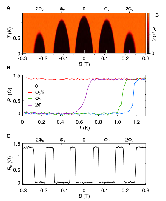
As a result of fluxoid quantization, the critical temperature, , of a cylindrical shell is periodically modulated by an axial magnetic field Tinkham1966 ; Little1962 . For cylinders with radius smaller than the superconducting coherence length, is expected to vanish whenever the applied flux (axial magnetic field component times shell cross-sectional area) is close to an odd half-integer multiple of the superconducting flux quantum, ( mTm2, ) deGennes1981 ; Schwiete2009 ; Dao2009 . Throughout the extended range where vanishes, superconductivity is destroyed Liu2001 ; Sternfeld2011 .
The nanowire used in device 1 has a hexagonal InAs core with diameter of nm and Al shell with thickness of nm, giving a mean diameter of nm. The dirty-limit coherence length is given by Tinkham1966 ; Gordon1984 . The measured normal state resistance is . The distance between the voltage probes is nm. This yields shell resistivity of nm , with the shell cross-sectional area nm2. The Fermi velocity in Al is m/s Kittel2005 , giving a Drude mean free path of nm, where is electron mass, is electron charge and is charge carrier density, with Fermi wave vector . The measured critical temperature is K. This gives nm, greater than the mean nanowire radius ( nm), hence the measured nanowires are expected to exhibit a destructive regime. This is consistent with the measurements, see Fig. S2A.
At integer flux quanta ( and ), normal-to-superconducting transitions appear as the temperature is lowered, with the critical temperature decreasing as the flux number increases. Around and the resistance of the shell, , stays at the normal value down to the lowest measured temperature, mK, as shown in Fig. S2B. At the base temperature, the two destructive regimes can be identified by abrupt changes of from to and then back to when the flux passes and , see Fig. S2C.
XV Penetration depth
An applied magnetic field penetrates thin-film superconductors with thickness much less than penetration depth, , uniformly. In dirty limit, the effective penetration depth , where and at zero temperature are related by Tinkham1966 . Taking as the London penetration depth for Al Kittel2005 , yields nm greater than Al thickness (30 nm). As a result, the flux in the wire is not quantized. Note, however, that the fluxoid is still quantized Little1962 ; Tinkham1966 .
XVI Tunneling spectroscopy
For all four tunneling-spectroscopy devices (1, 3, 4 and 5) the zeroth lobe, where the winding number is 0, shows a hard gap and no subgap states are visible. In the first lobe, with the phase winding of , the spectrum for devices 1, 3 and 4 (all with nm Al shell) displays a discrete, zero-energy state (see main-text Fig. 2, and Figs. S5 and S6), whereas for device 5 (with 10 nm Al shell) the spectrum consists of multiple discrete, but finite energy subgap states, see Fig. S7. In the second lobe, with even number of phase windings, the spectrum for device 1 features an asymmetric superconducting density of states with the lowest energy subgap state centered around eV, see Fig. S3; For devices 3 and 4, multiple subgap states can be identified at finite voltage, but no zero-bias peak, see Figs. S5 and S6; For device 5, a qualitatively similar to the first lobe spectrum with several finite-energy states is observed, see Fig. S7. Device 4 with slightly bigger diameter, displays the third lobe, with odd number of phase windings. The spectrum features subgap states and a peak at zero bias, see Fig. S6.
For device 5, a discrete state crosses zero-energy around V and then again at V, resembling a proximitized quantum dot state, similar to the one previously studied in Ref. Lee2013 , see Fig. S7. We usually associate such state with a resonant level in the barrier and if possible avoid it in the measurements.
XVII Model for the disordered superconducting shell
In this Section, we consider a disordered superconducting shell (e.g., Al shell) with inner and outer radii and , respectively, see Fig. 3 of the main text. We assume that the thickness of the shell , with being the London penetration length in the bulk superconductor. In this case, the screening of the magnetic field by the superconductor is weak and can be neglected. The effective Hamiltonian for the SC shell in cylindrical coordinates can be written as
| (6) |
Here, are the electron momentum operators, the electric charge, the electron mass in the SC, , is the chemical potential in the SC, are Pauli matrices representing Nambu space, is bulk SC gap at , is the winding number for the SC phase, and represents short-range impurity scattering potential. It is enlightening to perform a gauge transformation which results in a real order parameter, i.e. . The gauge transformation introduces an effective vector potential, with
| (7) |
where and . It follows from this argument that the solution of Eq. (6) should be periodic with , see Fig. S8. Namely, the winding number adjusts itself to the value of the magnetic field so that the energy of the superconductor is minimized. In particular, for each winding number , the maxima of the quasiparticle gap occur at
| (8) |
We neglect the Zeeman contribution since the typical magnetic fields of interest are smaller than mT for which the Zeeman splitting is negligible.
In order to understand the magnetic field dependence of the quasiparticle gap, one needs to calculate the Green’s functions for the disordered SC shell as a function of . The disordered superconductor is characterized by an elastic mean free path and a corresponding diffusive coherence length , where is the coherence length in the bulk, clean limit ( is the Fermi velocity in the SC). For simplicity, we assume henceforth that the thickness of the superconducting shell 111our results also apply to the case of and , so that the properties of the system can be obtained by calculating the Green’s function for the disordered bulk superconductor in magnetic field and . This problem was considered by Larkin Larkin1965 , who showed that within the self-consistent Born approximation the normal and anomalous Matsubara Green’s function are given by
| (9) | |||
| (10) |
where and is the angular momentum eigenvalue and is the eigenvalue of the Hamiltonian
The functions and are determined by the following equations:
| (11) | |||
| (12) |
with being the elastic scattering time and being the angular momentum cutoff. In the limit , the leading order corrections to the above equations appear in quadratic order since linear terms vanish due the averaging over . Indeed, one can show that the self-consistent solution for is given by
| (13) | ||||
| (14) | ||||
| (15) |
where is the characteristic scale for the magnetic field effects in the problem. Here . Thus, corrections to the pairing gap are governed by the small parameter . In terms of the flux quantum, this condition reads . Note that disorder suppresses orbital effects of the magnetic field and leads to a weaker dependence of the pairing gap on magnetic field (i.e., quadratic vs linear). In other words, the disordered superconductor can sustain much higher magnetic fields compared to the clean one, see Fig. S8. Finally, the analysis above can be extended to . After some manipulations, one finds that Liu2001 ; Koshnick2007
| (16) |
This estimate is consistent with the numerical calculations, see Fig. S8.
XVIII Derivation of the effective Hamiltonian
In the previous Section we derived the Green’s function for the disordered superconducting ring. One can now use these results to study the proximity effect of the SC ring on the semiconducting core. We will focus again on the case when the SC shell is thin such that . In this case, one can neglect magnetic field dependence of the self-energy for the entire lobe. Thus, one can use zero field Green’s functions for the disordered superconductor to investigate the proximity effect which are obtained by substituting and with in the clean Green’s functions.
One can now integrate out the superconducting degrees of freedom and calculate the effective self-energy due to the tunneling between semiconductor and superconductor. Using the gauge convention when is real, the tunneling Hamiltonian between SM and SC is given by Stanescu2011
| (17) |
where and refer to the SM and SC domains, respectively. is the tunneling matrix element between the two subsystems, and and are the fermion annihilation and creation operators in the corresponding subsystem. One can calculate the SC self-energy due to tunneling to find
| (18) |
where is a quickly decaying function away from describing tunneling between the two subsystems. Note that the SC self-energy in this approximation is the same as for a clean superconductor because the ratio of is independent of .
The Green’s function for the semiconductor can be written as
| (19) |
In order to calculate quasiparticle energy spectrum one has to find the poles of above Green’s function.
In the hollow cylinder limit, is a constant and one can find low energy spectrum analytically. Indeed, after expanding Eq. (19) in small , the quasiparticle poles are determined by the spectrum of the following effective Hamiltonian:
| (20) |
By comparison with Eqs. (6)-(10) of the main text, one can establish the correspondence between the bare parameters of the semiconductor and the renormalized parameters of the hollow cylinder model due to the proximity cooupling to the SC. We find:
| (21) | |||||
| (22) | |||||
| (23) | |||||
| (24) |
where , and are the bare values of the effective mass, chemical potential and spin-orbit coupling strength, respectively. Specifically, note that the renormalizaiton also reduces the Fermi velocity by a factor of which is well-known to lead to shorter coherence lengths than from naive estimates that assume bare Fermi velocities Stanescu2011 ; nadj2013 ; Peng2015 .
XIX Effect of higher states on the gap
As demonstrated in the main text, states with larger have the potential to close the gap and thus limit the extent of the topological phase. Here we provide analytical estimates within the hollow cylinder model for the regions in parameter space that become gapless due to higher states. We start with the BdG Hamiltonian (5) of the main text assuming ,
| (25) | ||||
with
| (26) | |||||
| (27) | |||||
| (28) | |||||
| (29) |
with . With respect to the main text, we also introduced anisotropic spin-orbit coupling with and representing the strength of coupling to the transversal and longitudinal () momentum direction. In the main text, we used isotropic spin-orbit but it is convenient for the discussion below to distinguish the two contributions.
Example energy spectra for the lowest sectors are shown in Fig. S9. Particle-hole symmetry relates and sectors. Therefore, sector is special in this sense. Note that is crucial to estimate the topological gap in the sector, i.e., a topological gap requires and . The conditions for a finite gap in sectors are more stringent. First of all, the pairing term hybridizes states within each sector. Thus, the system is gapless if there is an odd number of particle and hole bands at the Fermi level, which leads to the condition
| (30) |
which follows from the gap closing at . The gapless region in the upper right corner of Figs. 3, A and B, of the main text is due states fulfilling condition (30).
If condition (30) is not satisfied and the number of bands at the Fermi levels is even, the system can be gapped – see, for instance, panels (b) and (c) in Fig. S9. This happens, for example, if the effective chemical potential for a given subband in which case the subband is empty and gapped. However, if the subband is filled, i.e. if , one has to investigate the closing of the gap at finite momenta. In this case, the system is gapless when is smaller than a certain critical value required to hybridize particle and hole bands with mismatched Fermi momenta, see Fig. S9, (b) and (c). In the limit , the condition for a vanishing gap reads
| (31) | ||||
| (32) |
One may notice that the term acts as a Pauli limiting field for a given subband and leads to pair-breaking effects.
We can understand the generally finite extent of the gapped regions in the - plane by considering conditions (31) and (32). Condition (31) is either met for sufficiently large or sufficiently large (when is kept constant). At the same time, large states generally violate condition (32) since the bottom of the band is shifted up which needs to be compensated by sufficiently large . We therefore expect to find gapless states for large (which enable large ) or very large which fulfill condition while still being compatible with condition .
XX Phase diagram in the second lobe
In Fig. S10 we simulate the topological phase diagram and Majorana coherence length in the second lobe. We find that for the parameters of the transport simulations in the main text, the system is in the topologically trivial phase in the second lobe. In general, we find that topological phases in the second lobe have extremely small gap and therefore also very long Majorana coherence lengths.
XXI Coulomb spectroscopy
The Coulomb peak spacing is dictated by the lowest energy state at energy , may it be a subgap state or the superconducting gap itself. The periodicity of the Coulomb peaks is determined by the ratio between and the charging energy, . The Coulomb blockade is periodic for ; It becomes even-odd once is less than ; And it is periodic in case . Non-interacting Majorana modes have zero energy, hence a Coulomb island hosting Majoranas can be charged in portions of single electrons. If the wavefunctions of the opposing Majorana modes have a finite overlap, for example because of the finite island length, the energy of the corresponding modes will deviate from zero Albrecht2016 ; vanHeck2016 .
In the even-odd Coulomb blockade regime, the Coulomb-peak spacing, , is proportional to for even diamonds and for odd diamonds, which implies that Albrecht2016 ; Higginbotham2015 . This makes the Coulomb spectroscopy a powerful tool to study the interaction of Majorana modes in hybrid superconducting islands with finite size.
Device 2 consists of six hybrid islands with lengths ranging from nm up to nm. Figure 6 in the main-text presents measurements for the shortest island. Data for the other five islands are presented in Figs. S11–S15. In each of the figure, panel (A) displays the scanning electron micrograph with the measurement setup for corresponding island highlighted in false colors; Panel (B) shows zero-bias conductance as a function of the axial magnetic field, , and gate voltage, ; Panel (C) depicts average even and odd peak spacing evolution in magnetic field, extracted from the data shown in panel (B); Panels (D) and (E) show Coulomb diamonds in the middle of the zeroth and first lobes, the later featuring zero-bias peaks at the degeneracy points for each island.
The same measurement routine was carried out at several different gate configurations for each island to gather more statistics. The average lever arm, , the difference of average even and odd peak spacings as well as the corresponding amplitude —all measured at mT—are given in Table 1.
A set of additional data from device 2 measured on the nm Coulomb island at V is shown in Fig. S16. For comparison, the data from the same island presented in Fig. S12 is taken at V. Similar to the other island lengths, -periodic Coulomb diamonds are found in the zeroth lobe (Fig. S16C); In the destructive regime, the superconducting gap is suppressed and the Coulomb blockade becomes periodic with the degeneracy points displaying normal density of states (Fig. S16D); In the first lobe, the diamonds are nearly -periodic with discrete, low energy states at the degeneracy points (Fig. S16E); In the second lobe, the superconductivity is restored (see Fig. S2), however, the Coulomb blockade is periodic and no clear discrete states can be resolved (Fig. S16F). Qualitatively similar behavior is observed for all six island lengths.
XXII Peak spacing analysis
An exemplar routine of the peak spacing analysis is illustrated in Fig. S17 for data from device 2 measured on the nm Coulomb island. The peak positions and spacings are deduced from a multi-Lorentzian fit to the data. A sharp distinction between the destructive regime and the first lobe is found: While the peak spacing evolution with the plunger-gate voltage is featureless at mT (blue line in Fig. S17A), a clear zigzag-like alternating pattern between the adjacent spacings emerges at mT (green line in Fig. S17B). The destructive regime, where the Coulomb blockade is periodic, provides a useful tool for calibrating the analysis and determining the experimental noise floor.
Conductance line shape of the Coulomb oscillations in the regime (tunneling rate to the leads) (electron temperature) (level spacing) (charging energy) is given by (see Ref. Beenakker1991 )
| (33) |
where is the amplitude of the peak, is the peak position and is the peak width parameter that is related to the electron temperature by , with the lever arm . The Full width at half maximum of the peak is given by 3.5 .
Figure S17C shows three Coulomb peaks measured at mT and fit to a linear combination of Eq. (33) with the parameter estimates and their standard errors given in the figure caption. The average peak width mV together with the lever arm meV/V, deduced form the Coulomb diamonds shown in Fig. S17E, yield electron temperature mK. Note that the effective electron temperature is two orders of magnitude higher than the standard fit error of the peak-position estimate.
XXIII Distinguishing topological from trivial regime
In this section we compare simulated observables in the topological and in the trivial regime. For this purpose, we perform transport simulations in different locations of the phase diagram, see Fig. S23. From these simulations, it is clear that a ZBP is not a unique signature of the topological phase. For example, a very small bulk gap might mimic a faint ZBP as in Fig. S23B. Furthermore, crystalline symmetries might stabilize additional topological phases with an even number of MZMs at each end, see Fig. S23D. Therefore, we also calculate the lowest excitation energy for different wire lengths in Fig. S24, similar in spirit to the experimental Coulomb blockade spectroscopy. We find that only topological phases with a large gap show an exponential decay of the lowest excitation energy over a large range of wire lengths, consistent with localized end states. Fig. S24C corresponds to a scenario with even number of MZMs at each end (two in this case) protected by a spatial mirror symmetry. Initially the behavior is exponential for short wire lengths but flattens out at longer wire lengths. Due to limited numerical accuracy the mirror symmetry is slightly broken in our system and the two MZMs are not at exactly zero energy. Analogous, any spatial symmetry will be broken in an experiment due to imperfections. As we have shown here with multiple different scenarios, it is possible to distinguish trivial from topological ZBPs with this technique.


![[Uncaptioned image]](/html/2003.13177/assets/x23.png)

| (nm) | (meV/V) | (mV) | (eV) |
|---|---|---|---|
| 210 | 4.9 | 9.3 | 45 |
| 300 | 6.1 | 2.5 | 15 |
| 420 | 11 | 0.91 | 10 |
| 620 | 17 | 0.17 | 3 |
| 810 | 17 | 0.08 | 1.4 |
| 970 | 15 | 0.04 | 0.6 |