One-dimensional moiré charge density wave in the hidden order state of URu2Si2 induced by fracture
Abstract
Moiré patterns can lead to fundamentally new electronic behavior when formed between two atomic lattices slightly shifted with respect to each otherBistritzer and MacDonald (2011); Cao et al. (2018); Xie et al. (2019); Choi et al. (2019); Jiang et al. (2019); Lu et al. (2019); Peng et al. (2019). A solid is however not just characterized by the atomic lattice, but also by dynamical charge or magnetic excitations that do not need to be commensurate to the lattice. This raises the question if one can obtain a moiré through the interaction of dynamic modes with the atomic lattice. Here we report on the discovery of a one-dimensional charge density wave (1D-CDW) which is a moiré pattern between the atomic lattice and a hot spot for electronic scattering in the bandstructure of the hidden order (HO) state of URu2Si2. The moiré is produced by fracturing the crystal in presence of a dynamical spin mode at low temperatures. Our results suggest that charge interactions are among the most relevant features competing with HO in URu2Si2.
The HO state of URu2Si2 puzzles experimentalists and theoreticians alike since its discovery more than three decades ago Flouquet (2005); Mydosh and Oppeneer (2011); Mydosh et al. (2020). It consists of a phase transition below K in which there is a large entropy changeWang et al. (2020). However, neutron scattering experiments do not show any sign of static magnetic nor structural orderBourdarot et al. . Instead, there are dynamical modes of Ising-like magnetic excitations with a strong fluctuating magnetic moment, , located at and Broholm et al. (1987, 1991); Bourdarot et al. . These modes are quenched into an antiferromagnet order above 5 kbar with the wavevectorBourdarot et al. ; Mydosh et al. (2020); Villaume et al. (2008) and with the wavevector at high magnetic fieldsWiebe et al. (2007); Villaume et al. (2008); Knafo et al. (2016). The magnetic field also modifies the Fermi surface, producing nesting at Pourret et al. (2013). In addition, several measurements indicate that at zero field the bandstructure has a hot spot for scattering at , so that there is a strong interaction between electronic degrees of freedom and the dynamical modesElgazzar et al. (2009); Pourret et al. (2013); Wiebe et al. (2007); Morr (2016). Here we use Scanning Tunneling Microscopy (STM) to study high quality single crystals of URu2Si2. Contrasting previous STM workAynajian et al. (2010); Schmidt et al. (2010), we find that there is a one-dimensional charge modulation with a wavevector that is a moiré combination of the atomic lattice periodicity and the dynamical spin excitation mode at . This suggests that the dynamical modes can lead to new symmetry breaking ground states in URu2Si2 through external action.
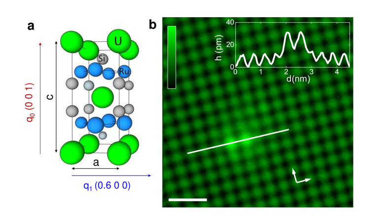
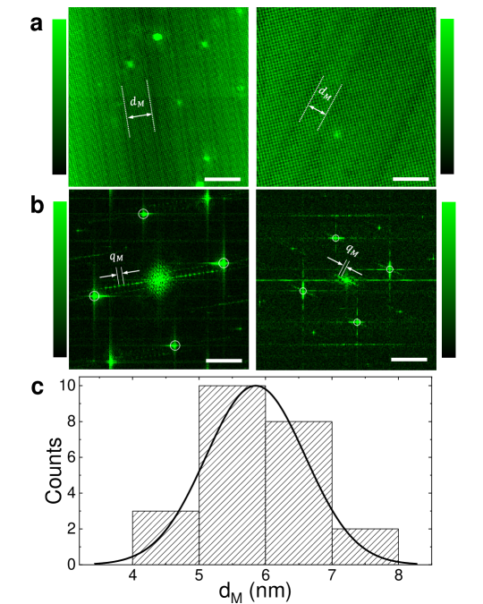
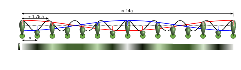
Figure 1(a) shows the crystal structure of URu2Si2 together with a representation of the directions of and . In Fig. 1(b) we show atomically resolved images of the U square atomic lattice, with the in-plane lattice parameter pm, similar as in previous work Aynajian et al. (2010); Schmidt et al. (2010); Zhang et al. (2018). We focus here mostly on features obtained from the STM topography. Spectroscopic features are mentioned in the supplementary information and mostly coincide with previous work.
In fields of view that are sufficiently large and free of steps, there is a certain pattern which repeats on the image and is one-dimensional (Fig.2). The pattern corresponds to height changes which vary from place to place and are very small, of at most 2 pm,i.e. 1% or less as compared to the usual atomic corrugation (inset of Fig. 1b, Aynajian et al. (2010); Schmidt et al. (2010); Zhang et al. (2018)). The period and the direction of the one-dimensional pattern can be determined from the Fourier transforms of the topographic images. The Bragg peaks associated to the one-dimensional modulation repeat at integer multiples of . We determine from the reciprocal space distance between consecutive peaks and obtain that nm (Fig.2b). This corresponds to a modulation of period nm (). The one-dimensional modulation is nearly parallel to an in-plane crystalline direction, often with a small angle of a few degrees. A histogram with observed is shown in Fig. 2c. We observed the modulation in many fields of view on five different samples, each one cleaved at low temperatures (more details in the Supplementary Information), up to magnetic fields of 4 T and temperatures several K above liquid helium. At higher temperatures and above THO we were unable to detect it because the amplitude of the modulation is too small to detect in presence of temperature induced drift in the STM. As discussed in the Supplementary Information in detail, the observed features are associated to fracturing the sample at low temperatures.
A modulation observed in STM topographic images superimposed to the atomic lattice is usually caused by charge order in form of a CDW. The Fermi surface has mainly a four-fold symmetry and there are no features in the Fermi surface which could lead to any 1D-CDWElgazzar et al. (2009); Bourdarot et al. (2010). Features of the Fermi surface are instead fourfold, showing nesting at along the c-axis. Nesting occurs in-plane at too at sufficiently high magnetic fieldsPourret et al. (2013). At the level of the local atomic size density of states measured by in-plane topographic imaging with STM, we do not expect to observe directly modulations at wavevectors corresponding to dynamical modes. However, we might be sensitive to effects related to the mode at , which is clearly an in-plane hot spot in the Fermi surface. As we show in the following, is related to through a moiré pattern and the direction of is determined by the direction of the propagation of the crack front during fracture.
First, let us establish the relation between and , knowing that . The superposition of 1D modulations with similar periodicities and () leads to an additional modulation, the moiré pattern, at a scale which is far above and and is given by Zhou et al. (2008); Oster and Nishijima (1963). If and with an integer (and of course ), the moiré adopts a ”fractional” form and . The moiré is then composed of cosine functions of wavelength phase-shifted to each other by . In STM images made at constant tunneling current, we measure the variations in the local density of states (LDOS) integrated between the Fermi level and the bias voltage as a function of the position. The LDOS can be understood as a combination of localized orbitals and itinerant electronsTersoff and Hamann (1983, 1985). Let us take for simplicity the case of a 1D row of atoms, separated by a given lattice constant. If there is a very weak modulation at a wavevector close to an integer times the lattice constant superposed to the 1D atomic lattice, the visible signature of this modulation on the LDOS is formed by the moiré pattern resulting from the value of the modulation at the atomic lattice positions. Let us consider schematically a set of elongated atomic orbitals located at integer multiples of and assume that the size of the lobes is given by a modulation close to (at (0.57 0 0), which gives , with the modulation at , , and ). The result is schematically shown in Fig. 3. The size of the lobes leads to a pattern which consists of two inverted cosines, each one with a periodicity and shifted by . Thus, our images show CDW at as a consequence of a moiré combination between and the atomic lattice.
Second, to understand the symmetry breaking, let us discuss the origin of the modulation. The modulation is not present in any of the STM images shown in Ref.Aynajian et al. (2010); Schmidt et al. (2010), although their resolution was of the same order as ours. In those experiments, samples were cleaved at relatively high temperatures (of the order of liquid nitrogen), whereas we cleave our sample at very low temperatures (below liquid helium). Cleavage of a hard single crystal is equivalent to brittle fracture. It is a fast procedure by which the bonds are broken first on one side of the sample and then a crack front travels through the sample in a short amount of time. The propagation of the crack front during cleavage leaves permanent modifications of the surfaceDeegan et al. (2003). These modifications can be due to acoustic waves that are emitted when a crack front crosses defects during the cleaving process or due to other forms of local interaction of the crack front and the crystalline lattice and have been extensively studied in materiales such as Si, sapphire or tungstenSherman and Be’ery (2004); Deegan et al. (2003); Kermode et al. (2013); Zhao et al. (2018). From a careful optical and electron microscopy analysis of surfaces of URu2Si2 broken at room temperatures and at low temperatures (see Supplementary Information) we obtain that samples cleaved at low temperatures have a set of linear features created during crack and oriented close to a crystalline axis. These features define a fixed direction which is close to one of the main in-plane crystalline axis and produce the one-dimensional symmetry breaking field. We note that we observe the modulation in five samples cut differently, each one with slightly different shapes, different crack initiation points, and different internal structure of defects.
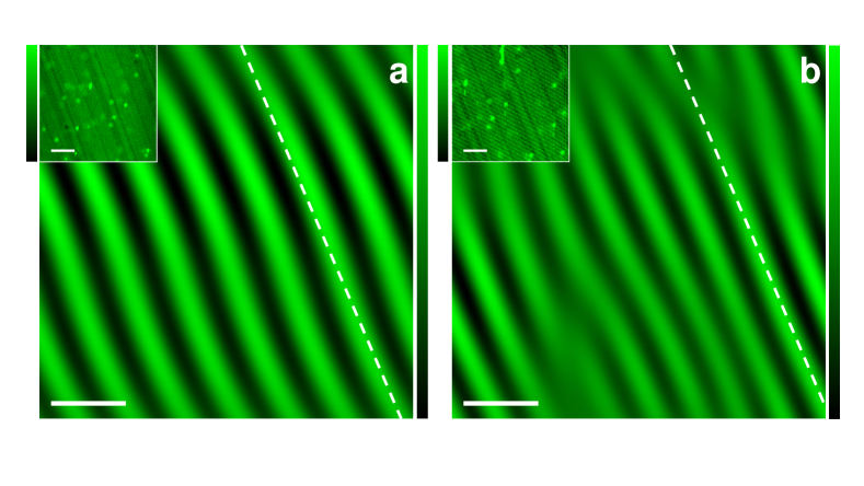
The modulation is not perfect over the whole crystal but shows defects at a few locations. Such a situation occurs in Fig. 4, where we filter the peaks corresponding to the modulation at to obtain Fig. 4a,b. We observe that, in these fields of view, the stripes are structured. In Fig. 4a there is a shear shift of the charge modulation. In Fig. 4b there is a pair of dislocations in the charge modulation in the top of the image and another dislocation in the bottom of the image.
Our scans show the 1D-CDW Bragg peaks just at the center of the Fourier transform. To understand this observation, let us describe a CDW through a vector , with the vector of the absolute value of the modulation, the wavevector of the modulation and a phase shiftEl Baggari et al. (2018). As we show in the Supplementary Information, the corresponding Fourier transform shows satellite peaks around lattice Bragg peaks when the displacement vector is in-plane along or . If the displacement is out-of-plane, , the image shows satellite peaks around the center of the Fourier transform. The latter is always observed in our images. Thus, we are mostly observing an amplitude modulation of the charge (out-of-plane), without in-plane atomic displacements.
Notice that there is no in-plane strain associated to the modulation, although the modulation might influence strain caused by defects. To analyze this possibility, we have calculated the strain from our images following Refs. Lawler et al. (2010); Zeljkovic et al. (2015). We can identify slight modifications of the strain built up around defects consisting of Si atoms on top of a U surface, with a tendency to form strain with a slightly elongated shape. It is useful to remind that Nuclear Magnetic Resonance (NMR) measurements highlight the relevance of charge disturbances and in particular show a two-fold lineshape on Si associated to defectsKambe et al. (2013, 2015, 2018). Our results suggest that Si defects are influenced by charge disturbances such as the one-dimensional charge modulation.
We should note that crack front velocity is of order of sound velocity (see Supplementary Information andSherman and Be’ery (2004); Deegan et al. (2003); Kermode et al. (2013); Zhao et al. (2018)). Thus, we can link together the external action (crack front), atomic displacement modes (phonons) and the electronic susceptibility of URu2Si2 (fluctuations at ). The phonon dispersion in URu2Si2 shows no strong features connected to the HO transitionBuhot et al. (2015). However, there is an anomalous phonon mode broadening which suggests strong anharmonicity and coupling to magnetic excitationsButch et al. (2015); Buhot et al. (2015); Gardner et al. (2016). The dispersion relation of the modes provides a velocity Buhot et al. (2015). Most remarkably, crack front velocity, sound velocity and the velocity of the magnetic modes are all of the order of tens of km/s.
Interestingly, the time required for each of these three modes to cross a single unit cell is in the femtosecond regime. Thus, ultrafast radiation experiments on surfaces of URu2Si2 might lead to similar effects as a travelling crack front and potentially to the nucleation of a similar CDW.
Notice that moiré patterns arise on surfaces or few layer systems because of displacements or rotations of atomic latticesBistritzer and MacDonald (2011); Cao et al. (2018); Xie et al. (2019); Choi et al. (2019); Jiang et al. (2019); Lu et al. (2019); Peng et al. (2019). Rotations among atomic layers provide a control parameter, the relative angle between layers, to modify the moiréCao et al. (2018). In our case, moiré modulations can arise with any characteristic vector from the electronic bandstructure. That is, with wavevectors located inside the Brillouin zone and lying close to an integer fraction of the unit cell lattice. To modify the moiré, we need to modify the bandstructure, with the usual control parameters as doping, stress or magnetic field. For very large values of in , the moiré pattern might rapidly acquire a very long wavelength, which should make it quite difficult to distinguish from a large defect or distortion. However, for small (and with a sufficient difference between and ), the moiré combinations proposed here could lead to a variety of new ground states.
In summary, we observe that the high susceptibility of URu2Si2 at results in quenched 1D-CDW when there is a sufficiently strong interaction with a cracking process. But we are not just condensing a CDW related to through fracture. The moiré between the atomic lattice and the modulation leads to a real, physical, 1D-CDW which breaks the in-plane square C4 symmetry. Of course such a CDW is not a property of the HO. But it is related to HO through one of the wavevectors that lead to the moiré. Our observation supports the claim that in the HO phase electric interactions might play a key role, as proposed by nuclear magnetic resonance experimentsKambe et al. (2018).
Acknowledgments
We acknowledge discussions with F. Guinea, A. Levy Yeyati and with S. Vieira and support by the Spanish MINECO (FIS2014-54498-R, MDM-2014-0377), by the Comunidad de Madrid through program NANOMAGCOST-CM (Grant No. S2018/NMT-4321) and by Cost Action CA16218 (Nanocohybri). I.G. acknowledges support by the European Research Council PNICTEYES grant agreement 679080. We also acknowledge the support of Departamento Administrativo de Ciencia, Tecnología e Innovación, COLCIENCIAS (Colombia) Convocatoria 784 - 2017 and the Cluster de investigación en ciencias y tecnologías convergentes de la Universidad Central (Colombia). We also acknowledge SEGAINVEX at UAM.
Author contributions
E.H. and I.G. spotted the one-dimensional modulation and worked through its characterization. The experiment was proposed by D.A. and J.F. and designed by E.H., I.G. and H.S.. V.B. searched for possible combinations of modulations, identified the moiré and calculated the strain, with the supervision of H.S., E.H. and I.G.. W.J.H. and J.A.G. provided support to the interpretation and in analyzing fracture, together with E.H. and with input from H.S.. J.C. made the corresponding simulations. D.A. prepared and characterized samples. The paper was written by E.H., I.G., J.F. and H.S. with contributions from all authors.
Methods
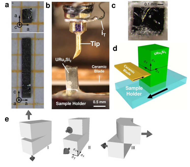
We use a STM set-up described in Refs.Suderow et al. (2011); Galvis et al. (2015) that features a movable sample holder which we use to cleave in-situ the sample and change in-situ the scanning windowSuderow et al. (2011). The single crystals of URu2Si2 have been grown by Czochralski method and have a residual resistance ratio of about 120 Aoki et al. (2010). We first screened crystals for high quality, from different growths and then cut crystals into needles of about 0.5 mm 0.5 mm 2 mm. We inserted each needle into a hole made on a gold substrate and glued them with silver epoxy. The needles were positioned into the sample holder in such a way that they hit a sharp ceramic blade when pulling on the sample holder. Slightly below 4.2 K we pulled on the holder through a manual mechanism located at room temperature and connected to the holder with a piano cord. We felt resistance when the sample touched the blade. We continued pulling until we heard a characteristic ”crack”. At this point, the sample was broken. The noise created during crack, which we heard outside the dilution refrigerator, evidences generation of sound waves during fracture. This was made with the tip far from the sample. We then approached the tip to the sample, scanned and obtained the results discussed here. We provide results obtained in five succesful cleaves, obtaining each time atomically flat surfaces in cryogenic vacuum. In each crystal, we were able to study several tens of scanning windows, each limited by the scanning range of our piezotube (2m 2m)Suderow et al. (2011). We present almost exclusively topographic STM images made at 150 mK and with the STM on constant current mode held by a feedback loop, with a setpoint of a fraction of nA and at a bias voltage of order of 10 mV.
Supplementary Information
.1 Further details of the experimental set-up and results on five samples
The STM set-up has been described in detail elsewhereSuderow et al. (2011). However, it is useful to provide details about the additions that we have made to be able to cleave at low temperatures hard samples as URu2Si2. In Fig. 5a we show pictures of URu2Si2 from the side and from the top. The sample has been shaped using a wire saw into a rectangle elongated perpendicular to the cleaving plane (the (a,a) axis). In Fig. 5b we show a picture of the sample mounted on the STM. The picture is taken from the front. The piezotube is located on the top of the picture. We can see the tip of Au on the top of the image and the part of the URu2Si2 that holds out from the sample holder. A cleaved surface is shown in Fig. 5c from the top. In Fig. 5d we schematically show the process of cleaving. We move laterally the sample holder and a ceramic blade pushes laterally the rectangular sample until it breaks. The efforts during the crack are tear, compressive and shear efforts, as schematically represented in Fig. 5e.
The tip of Au is prepared and shaped as shown in Refs. Rodrigo et al. (2004); Suderow et al. (2011). To this end, we glue a pad of Au on the sample holder in such a way that we can move the tip between sample and pad of gold, once the sample has been cleaved. To analyze the images we use WSxM Horcas et al. (2007) and software available at Sof .
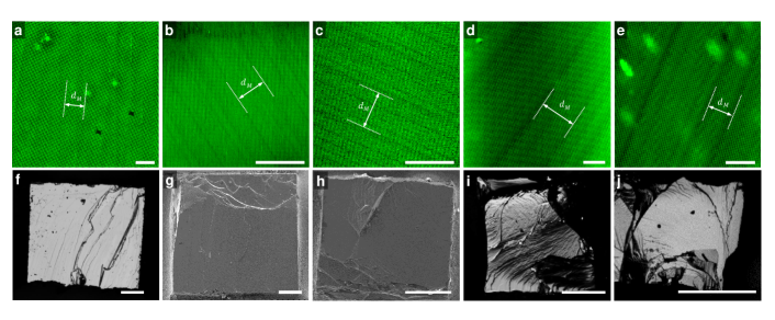
In Fig.6 we show results obtained in five different samples that were cleaved at low temperatures. We see that we can observe the one-dimensional modulation in each sample. The resulting cleaved surfaces are varied. Optical inspection mostly shows large mirror shiny surfaces (Fig.6f,g,h) or mirror like surfaces interspersed with large cracks (Fig.6i,j). In spite of that we could always obtain atomic resolution and the one-dimensional modulation.
.2 Analysis of fractured surfaces
After the experiment, we verified that the only source for the cracking noise was the sample (no components of the dilution refrigerator or the STM were damaged). The remaining part of the sample generally flew away to the bottom of the vacuum chamber. We collected both parts of the sample and made a detailed analysis of their surface using Scanning Electron Microscopy (SEM) and optical microscopy at room temperature.
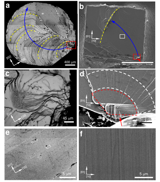
In single crystals, fractures are the result of the external applied stress, the elastic properties of the crystal and the relative orientation between the crack propagation and the crystalline lattice directions. As a result, characteristic surface marks can be identified to reconstruct the fracture process. We have made a microscopy study of surfaces on URu2Si2 obtained after cleaving at room temperature and at low temperatures (Fig. 7). We identify with yellow dashed lines step hackles. In both cases, hackles follow an elliptical shape. The crack front travels along a direction perpendicular to the hackle linesKermode et al. (2013); Zhao et al. (2018); Sherman (2003). The curved crack direction results due to the deflection of the crack between planes because of the anisotropic velocity depencence of lattice vibrationsSherman and Be’ery (2004). In our case, the crack front in the sample cleaved at room temperature can be approximated by an ellipse of semi-axes of and . From such a shape we can estimate the propagation velocity of the crack front to be of order of Kermode et al. (2013); Zhao et al. (2018); Sherman (2003). The sample cleaved at low temperatures is too small to make an estimation, but we can expect similar crack front velocities.
In the sample cleaved a room temperature we found that it was not easy to identify the starting crack point. Instead we observe a starting crack zone of approximately a few (red rectangle in Fig. 7a and Fig. 7c). By contrast, on the sample cleaved al low temperature, we identify the starting crack point as the red arrow in Fig. 7d. In every crack, we can identify the primary surface marks, called mirror and mist zones. These are regions where a crack radiates outwards from the starting point of fracture. These zones are the transition regions between the starting crack point and the hackle lines. We define the mirror zone by the region enclosed by the red dashed line (Fig. 7d). Inside the mirror zone we identify radially outgoing lines. Outside, in the mist zone, lines start to become straight and oriented with the crystalline axis, ending up in hackle lines. Hackle lines run in the local direction of craking and separate parallel but non coplanar sections of the fractured surface. Twist hackles are formed when the crack runs parallel to a preferent cleaving plane and the direction of the normal stress to this plane changes. Then, the crack cannot tilt in response to the new direction of stress direction and thus it splits into small, separated segmentsQuinn . These lines form at exactly 90∘ to each other and are often close to being parallel to a cristalline axis. The lines evidence the large accumulation of strain before the crack (see also Fig.8).
In order to address with more accuracy the crack features on the cleavage surfaces on both samples, we focus our attention in areas less than 25 25 (Fig. 7e,f). There we can observe important differences. In the sample cleaved at room temperature we identify flat surfaces of tens of microns with rectangular defects within areas of sizes 1-2 that are parallel to the [10] and [01] directions (Fig.7e). In the sample cleaved at 4.2K, by contrast, we observe stripes nearly parallel to the [01] atomic direction (Fig.7f). These stripes are formed hackle lines that run close to a crystalline axis. These are related to the travelling direction of the crack front. The interaction of the crack front with dynamical modes of URu2Si2 defines the moiré one-dimensional charge modulation discussed in the main text.
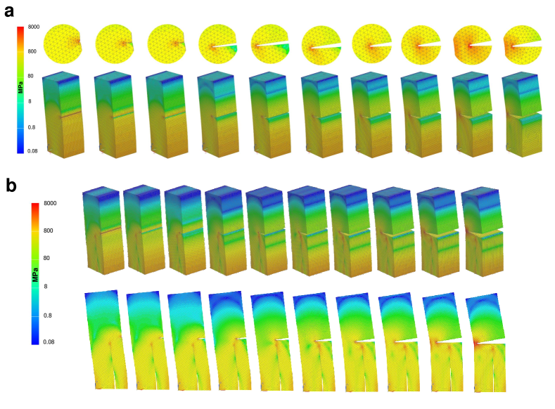
The establishment of any permanent modification of the crystal structure requires energy. The only available source is the strain energy dissipating during cleavage, which is used to create the new surfaces obtained after cleaving. It is useful to discuss the strain we accumulate before breaking the sample. To see this, we can consider that, when we use samples of 1 mm square section (instead of 0.5 mm), we break a tin solder joint of the pulling mechanism instead of the sample. By decreasing sample thickness to 0.5 mm we break instead the sample. Thus, we can estimate that the uniaxial force on the sample is of order of the shear force of a tin solder joint. A good estimate is probably between 1 and 10 kg, say 5 kg or 50 N. This is applied as a shear to the sample using a wedge. The uniaxial pressure is as high as 200 kg/mm2, if we estimate that contact between the wedge and the sample is along an area of 0.1x0.5 mm2. This produces as much as 20 kbar uniaxial pressure, enough to locally drive the system into an ordered phase close to the wedgeMydosh and Oppeneer (2011); Mydosh et al. (2020). More detailed calculations are provided in Fig. 8. We use a finite element calculation with the software NX Nastran. We use isoparametric tetrahedron elements with four vortex nodes and size additional midside nodes. The sample size is 1 mm 1 mm 3 mm and the mesh size is 50. We apply a lateral force of 50 N and a vertical tear force of 100 N, to be able to consider a sample separated in two parts in the model. We take a Young modulus of 192.85 GPaWang et al. (2020). We see that we can easily obtain locally pressures up to 80 kbar (8 GPa) at the wedge (Fig. 8a). We also see that, in presence of a large defect inside the sample, the local pressure is considerably enhanced and modified at the tip of the defect (Fig. 8b). This suggests that large sample anomalies, like cuts or twists, which remain unnoticed in usual characterization experiments such as resistivity or specific heat, strongly increase the likelihood of inducing permanent modifications during fracture.
When the sample cleaves, the pressure is of course released. However, there is a large amount of available energy from the accumulated strain. We can estimate the released energy and compare it to the bonding energy and find very large values, of order of the mJ. On the other hand, usually the tensile strength upon shear of the material is exactly the bond-breaking strength, plus the energy required to produce surface modifications. To have such a surplus of mechanical energy that does not go into bond-breaking and creates permanent features on the surface, we need that the lateral edge of the sample has a higher tensile strength than the bulk. This should indeed be the case, taking into account that the sample has been cut and has certainly many more defects close to the edge. As we see in Fig. 7, the surfaces obtained from cleaving an as-grown sample at room temperature are very different than those obtained cleaving a sample shaped using a wire saw at low temperature. The latter shows many more small scale modifications of the surface. Thus, the crack process has enough energy to produce permanent modifications of the surface. Furthermore, the local accumulated pressure drives the sample out of the HO state for the duration of the propagation of the crack front through the sample.
.3 Steps and the one-dimensional modulation
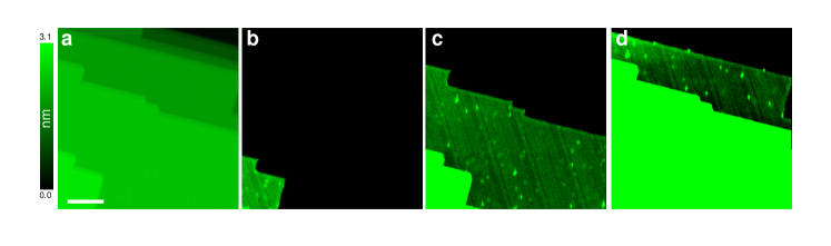
By contrast to the large steps observed using optical microscopy and SEM, it is interesting to analyze the one-dimensional modulation in atomically sized steps with STM. In Fig.9 we show a field of view with three large steps, each one consisting of a change in height of exactly half of the c-axis lattice constant. In the resulting plateaus, which are atomically flat, we can clearly see the modulation when we increase the contrast in the color scale that shows the topography (Fig.9b,c,d).
.4 Displacement vector
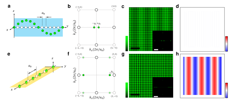
As we show in Fig. 10, the Fourier patterns of displacement vectors with different directions are different. We take , with wavevector . In Fig. 10a,c we show a modulation that occurs along the c-axis, out of plane (). In the Fourier transform Fig. 10b and inset of In Fig. 10c we observe a set of peaks around the center. When there is an in-plane displacement (Fig. 10e,g), the peaks in Fourier space appear around the Bragg peaks of the unmodulated atomic lattice (Fig. 10f and inset of g), without peaks at the center of the Fourier transform.
In our images of the one-dimensional modulation, we observe peaks at the center of the Fourier transform. Thus, we have a charge modulation exclusively along the c-axis, in the same way as the modulation mentioned above (Fig. 10a-d). Sometimes we also observe satellite modulation peaks around atomic Bragg peaks but with smaller amplitude that the peaks appearing at the center of the Fourier transform.
It is interesting to analyze the possibility of having lateral atomic displacements. To this end, let us start by remarking that when has in-plane components, atoms are displaced with respect to their equilibrium positions within the plane. We can thus define an in-plane field of displacements and describe the same modulation as displacements with respect to an undisturbed perfect lattice. If the wavevector of the modulation is sufficiently separated from the wavevector of the atomic lattice, we can obtain the displacements and the strain map , which is . The strain map can be normalized to the atomic lattice constant and shows quantitavely how much the atomic separation is reduced or extended in presence of a modulation or a defect. Let us see this in a couple of examples.
First, in Fig. 10a there is no in-plane strain (Fig. 10d), so that is equal to zero and we have a perfect square lattice. In a longitudinal modulation, by contrast, Fig.10e, there are in-plane atomic displacements and thus local strain (Fig.10h). The Fourier transform shows peaks indicating the direction of the modulation (here one-dimensional) surrounding the Bragg peaks of the atomic lattice, see Fig.10f. Let us now see how we calculate the strain maps of 10d,h.
The strain map can be obtained by operating on an image showing a lattice with strain. We define the atomic lattice as a periodic cosinusoidal modulation with amplitude and wavevector . Notice that we calculate the strain from a local displacement vector . To obtain we calculate . We chose in such a way as to be able to capture strain whose spatial variation is of order of . Of course, should be much larger than interatomic spacing and much smaller than the field of view. Then, , because the Gaussian weighting () occurs over a lengths scale that involve many interatomic distances, which eliminates the small wavelength contributions. We can then invert the cosine, taking care to correct for phase slips, and obtain . From we can reconstruct the strain free lattice and calculate the strain map (Fig.10d,h). This is a widely used algorith with many applications, including correction of drifts and measurement of strain in strained latticesLawler et al. (2010); Zeljkovic et al. (2015). In Fourier space, it corresponds to extract the Fourier components around the atomic lattice Bragg peaks along x and along y and shift these together down to the center of Fourier space. The result is that a strain map is visualized as a two-dimensional image, as shown for the above mentioned examples in 10d,h. Notice that can be calculated only at a distance from the border of the image.
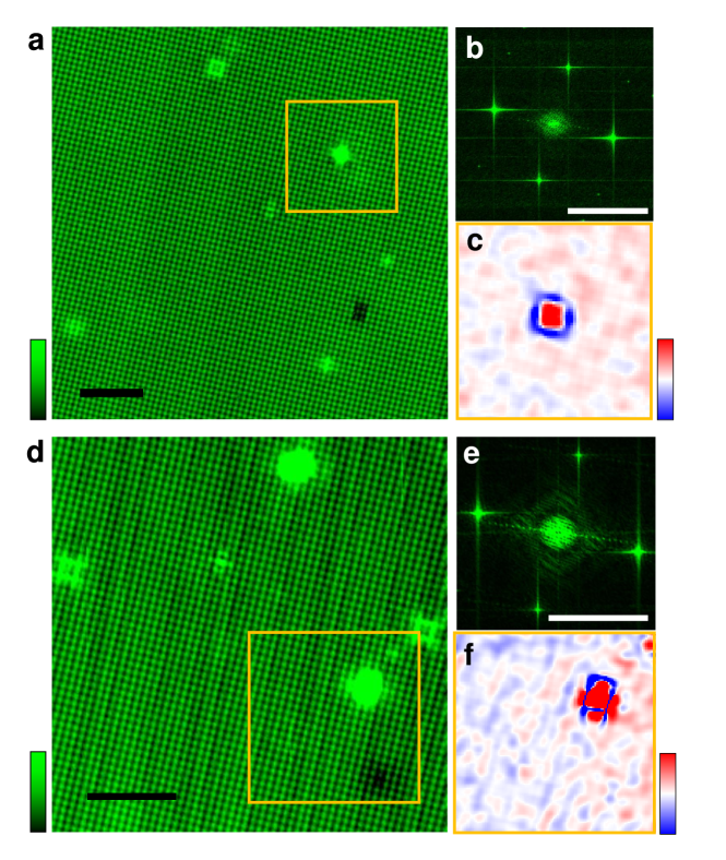
We can now apply such a reasoning to our data. As we discuss in the paper, in most cases the Bragg peaks associated to the modulation are centered at the origin. We rarely see a signal around the Bragg peaks and it is much weaker than the signal at the center. Therefore, the modulation has only a c-axis component and we indeed do not observe any strain. To test this with more detail we proceeded to the calculations and show the result in Fig. 11. Let us start with an image with a weak modulation (smaller corrugation) Fig. 11a. The one-dimensional modulation is seen in the Fourier transform Fig. 11b as a set of peaks at the center, with no clear signature around the Bragg peaks of the atomic lattice. The corresponding strain map is flat within our noise level, which we estimate to be of 0.1% the lattice constant . For comparison, the vertical displacement we can associate to the one-dimensional modulation is at most of 2 pm, which is 0.5% of the lattice constant . A pressure of 10 kbar corresponds to a modification of the lattice constant by about 1 pm.
Interestingly, we do observe an increase in the displacement around atomic size defects. We show around such a defect in Fig. 11c. The defect consists of a square of Si atoms on top of the U surface. The strain field is a square which follows the orientation of the Si atoms (at 45∘ with respect to the U lattice). It shows that the strain accumulates in the U lattice just around the defects. The interatomic distance between Si atoms is also modified. Let us now consider a field of view where the one-dimensional modulation has a slightly larger corrugation (Fig. 11d). The Fourier transform also shows mostly peaks around the center (Fig. 11e). When calculating we find a slight tendency to form one-dimensional stripe. Around a defect (11f) we identify here an asymmetry in the strain map around the defect. The compression and extension occurs preferentially along an axis that is parallel to the one-dimensional modulation. This shows that there is an interaction between the one-dimensional modulation and the strain field produced by individual defects.
.5 Bias voltage dependence of STM topographic images and spectroscopic features of the one-dimensional modulation
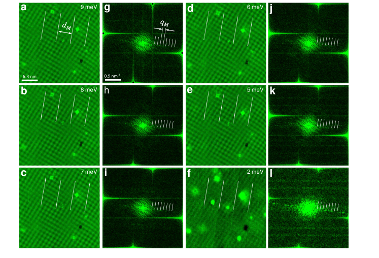
In Fig. 12 we show the bias voltage dependence of the modulation discussed in the main text. We focus here on topographic images taken in the range between 10 mV and 2 mV. In real space we see the one-dimensional modulation and a few atomic size defects. The Fourier transform shows the four Bragg peaks of the atomic lattice and the peaks corresponding to the modulation. In Fourier space we also observe a white circle, with structure inside, around the center. This is the consequence of quasiparticle interference scattering at the defects. Here we show topographic images, which are obtained at constant current. The current is given by where is the bias voltage given in the images and the density of states. Therefore, it provides an energy integrated account of the density of states between zero bias and the voltages mentioned at each image in Fig. 12.
The fact that the observed corrugation is so small suggests that the associated features in are very small too. Nevertheless, we can try to discuss the features in the spectroscopy, first remembering previous results Aynajian et al. (2010); Schmidt et al. (2010); Haule and Kotliar (2009) and comparing ours to those results and then analyzing in more detail in the low energy part of the data.
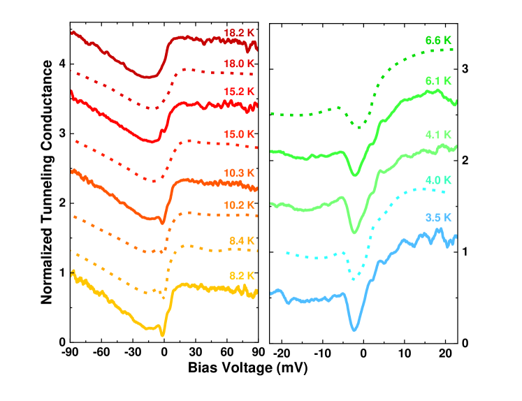
We first have to realize that the local density of states has no region in energy where it is flat. It consists of a Fano anomaly, superposed to a gap opening and of two van Hove singularities located at a few mV. To see this, let us start by comparing our work with previous results (Fig.13). As shown in Refs.Aynajian et al. (2010); Schmidt et al. (2010); Haule and Kotliar (2009), the local density of states in URu2Si2 has several interesting features whose evolution is strongly linked to the heavy fermion nature of URu2Si2 and the HO transition. When cooling from room temperature, the local density of states acquires an asymmetric shape. The asymmetric shape follows well a Fano-lineshape. The Fano-lineshape occurs due to interference from simultaneous tunneling into light and heavy bands. When cooling, the formation of the heavy bands is seen in the establishment of the Fano-lineshape in the local density of states. At about 18 K (see Fig.13), the resulting local density of states is explained by well established heavy electron bands Aynajian et al. (2010); Schmidt et al. (2010); Haule and Kotliar (2009). When entering the HO state, a feature appears close to zero energy. The feature develops when cooling into a V-shaped depression of the local density of states, which is asymmetric in bias voltage (see Fig.13) Aynajian et al. (2010); Schmidt et al. (2010); Morr (2016). As we see in Fig.13, we can exactly reproduce those previous results.
As shown in Refs.Aynajian et al. (2010); Schmidt et al. (2010); Morr (2016), the feature reflects the modifications in the bandstructure introduced by HO, observed thanks to enhanced quasiparticle interference induced by Th in doped samplesSchmidt et al. (2010). These can be associated to a gap opening due to nesting along when entering HO that provides the V-shaped depression. It was also previously shown that the establishment of the Fano-lineshape leads to peaks from the band hybridization in the local density of states. These are due to van Hove anomalies at the energies with strongest band bending that provide a large density of states Maltseva et al. (2009). These occur at particularly low energies in URu2Si2Morr (2016). In addition, there are two hybridized bandsMorr (2016); Yuan et al. (2012). These hybridization features occur below 2mV in form of several kinks in the bandstructure. Th doped samples show enhanced in-plane electronic scattering along a few wavevectors, some close to the wavevector providing a hot spot on the Fermi surfaceSchmidt et al. (2010).
It should be clear from the outset that any feature appearing in such a wavy background is very difficult to disentangle, particularly if associated to such a small signal in the topography. Below about 2 mV, we can identify some features in the spectroscopic maps. These are very weak and yet not fully clear, although worth to comment on.
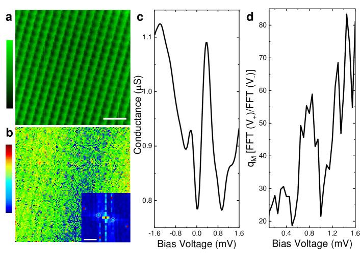
Some of these features are seen when zooming into data obtained in Ref.Aynajian et al. (2010); Schmidt et al. (2010) but these were mostly left undiscussed. Further analysis shown in Ref.Maltseva et al. (2009) related these features to the bandstructure. There are hybridized bands at very low energies with a bandstructure that is highly asymmetric with respect to the Fermi levelMorr (2016). We show our result in 14 on a field of view without defects. There are two clear peaks located at about -1.5 mV and at +0.4 mV. These peaks are at a a similar energy position as those found in previous work and related to the bandstructure. Here we observe that these are considerably more pronounced. As band hybridization leads to a highly asymmetric local density of states, we have chosen to divide the signal at positive with that at negative bias voltages. We then observe the modulation as a stripe which goes from the top left to the upper right part of the image. The Fourier transform shows the corresponding peaks, which show no dispersion with bias voltage, although their amplitude strongly varies. We observe that the amplitude decreases below about 1.6 mV. Furthermore, we observe an increase at about 0.8 mV (Fig. 14d). This can highlight a modification of the signal related to the one-dimensional modulation at a van Hove anomaly. Of course, a comprehensive understanding of all these features requires a careful analysis of the tunneling conductance and its temperature dependence, but this already establishes a link between the one-dimensional modulation and the local density of states.
References
- Bistritzer and MacDonald (2011) R. Bistritzer and A. H. MacDonald, Moiré bands in twisted double-layer graphene, Proceedings of the National Academy of Sciences 108, 12233 (2011), https://www.pnas.org/content/108/30/12233.full.pdf .
- Cao et al. (2018) Y. Cao, V. Fatemi, A. Demir, S. Fang, S. L. Tomarken, J. Y. Luo, J. D. Sanchez-Yamagishi, K. Watanabe, T. Taniguchi, E. Kaxiras, R. C. Ashoori, and P. Jarillo-Herrero, Correlated insulator behaviour at half-filling in magic-angle graphene superlattices, Nature 556, 80 (2018).
- Xie et al. (2019) Y. Xie, B. Lian, B. Jäck, X. Liu, C.-L. Chiu, K. Watanabe, T. Taniguchi, B. A. Bernevig, and A. Yazdani, Spectroscopic signatures of many-body correlations in magic-angle twisted bilayer graphene, Nature 572, 101 (2019).
- Choi et al. (2019) Y. Choi, J. Kemmer, Y. Peng, A. Thomson, H. Arora, R. Polski, Y. Zhang, H. Ren, J. Alicea, G. Refael, F. von Oppen, K. Watanabe, T. Taniguchi, and S. Nadj-Perge, Electronic correlations in twisted bilayer graphene near the magic angle, Nature Physics 15, 1174 (2019).
- Jiang et al. (2019) Y. Jiang, X. Lai, K. Watanabe, T. Taniguchi, K. Haule, J. Mao, and E. Y. Andrei, Charge order and broken rotational symmetry in magic-angle twisted bilayer graphene, Nature 573, 91 (2019).
- Lu et al. (2019) X. Lu, P. Stepanov, W. Yang, M. Xie, M. A. Aamir, I. Das, C. Urgell, K. Watanabe, T. Taniguchi, G. Zhang, A. Bachtold, A. H. MacDonald, and D. K. Efetov, Superconductors, orbital magnets and correlated states in magic-angle bilayer graphene, Nature 574, 653 (2019).
- Peng et al. (2019) L. Peng, J. Qiao, J.-J. Xian, Y. Pan, W. Ji, W. Zhang, and Y.-S. Fu, Unusual electronic states and superconducting proximity effect of Bi films modulated by a NbSe2 substrate, ACS Nano 13, 1885 (2019), https://doi.org/10.1021/acsnano.8b08051 .
- Flouquet (2005) J. Flouquet, On the heavy fermion road, Progress in Low Temperature Physics 15, 139 (2005).
- Mydosh and Oppeneer (2011) J. A. Mydosh and P. M. Oppeneer, Colloquium : Hidden order, superconductivity, and magnetism: The unsolved case of , Rev. Mod. Phys. 83, 1301 (2011).
- Mydosh et al. (2020) J. A. Mydosh, P. M. Oppeneer, and P. S. Riseborough, Hidden order and beyond: an experimental—theoretical overview of the multifaceted behavior of , Journal of Physics: Condensed Matter 32, 143002 (2020).
- Wang et al. (2020) L. Wang, M. He, F. Hardy, D. Aoki, K. Willa, F. J., and C. Meingast, Electronic nematicity in revisited, (2020).
- (12) F. Bourdarot, S. Raymond, and L.-P. Regnault, Neutron scattering studies on , .
- Broholm et al. (1987) C. Broholm, J. K. Kjems, W. J. L. Buyers, P. Matthews, T. T. M. Palstra, A. A. Menovsky, and J. A. Mydosh, Magnetic excitations and ordering in the heavy-electron superconductor , Phys. Rev. Lett. 58, 1467 (1987).
- Broholm et al. (1991) C. Broholm, H. Lin, P. T. Matthews, T. E. Mason, W. J. L. Buyers, M. F. Collins, A. A. Menovsky, J. A. Mydosh, and J. K. Kjems, Magnetic excitations in the heavy-fermion superconductor , Phys. Rev. B 43, 12809 (1991).
- Villaume et al. (2008) A. Villaume, F. Bourdarot, E. Hassinger, S. Raymond, V. Taufour, D. Aoki, and J. Flouquet, Signature of hidden order in heavy fermion superconductor : Resonance at the wave vector , Phys. Rev. B 78, 012504 (2008).
- Wiebe et al. (2007) C. R. Wiebe, J. A. Janik, G. J. MacDougall, G. M. Luke, J. D. Garrett, H. D. Zhou, Y.-J. Jo, L. Balicas, Y. Qiu, J. R. D. Copley, Z. Yamani, and W. J. L. Buyers, Gapped itinerant spin excitations account for missing entropy in the hidden-order state of , Nat Phys 3, 96 (2007).
- Knafo et al. (2016) W. Knafo, F. Duc, F. Bourdarot, K. Kuwahara, H. Nojiri, D. Aoki, J. Billette, P. Frings, X. Tonon, E. Lelièvre-Berna, J. Flouquet, and L.-P. Regnault, Field-induced spin-density wave beyond hidden order in , Nature Communications 7, 13075 (2016).
- Pourret et al. (2013) A. Pourret, A. Palacio-Morales, S. Krämer, L. Malone, M. Nardone, D. Aoki, G. Knebel, and J. Flouquet, Fermi surface reconstruction inside the hidden order phase of probed by thermoelectric measurements, Journal of the Physical Society of Japan 82, 034706 (2013).
- Elgazzar et al. (2009) S. Elgazzar, J. Rusz, M. Amft, P. M. Oppeneer, and J. A. Mydosh, Hidden order in originates from fermi surface gapping induced by dynamic symmetry breaking, Nat Mater 8, 337 (2009).
- Morr (2016) D. K. Morr, Theory of scanning tunneling spectroscopy: from kondo impurities to heavy fermion materials, Reports on Progress in Physics 80, 014502 (2016).
- Aynajian et al. (2010) P. Aynajian, E. H. da Silva Neto, C. V. Parker, Y. Huang, A. Pasupathy, J. Mydosh, and A. Yazdani, Visualizing the formation of the Kondo lattice and the hidden order in , Proceedings of the National Academy of Sciences 107, 10383 (2010).
- Schmidt et al. (2010) A. R. Schmidt, M. H. Hamidian, P. Wahl, F. Meier, A. V. Balatsky, J. D. Garrett, T. J. Williams, G. M. Luke, and J. C. Davis, Imaging the fano lattice to hidden order transition in , Nature 465, 570 (2010).
- Zhang et al. (2018) W. Zhang, H. Y. Lu, D. H. Xie, W. Feng, S. Y. Tan, Y. Liu, X. G. Zhu, Y. Zhang, Q. Q. Hao, Y. B. Huang, X. C. Lai, and Q. Y. Chen, ARPES/STM study of the surface terminations and -electron character in , Phys. Rev. B 98, 115121 (2018).
- Bourdarot et al. (2010) F. Bourdarot, E. Hassinger, S. Raymond, D. Aoki, V. Taufour, L.-P. Regnault, and J. Flouquet, Precise study of the resonance at q0=(1,0,0) in , Journal of the Physical Society of Japan 79, 064719 (2010).
- Zhou et al. (2008) S. Zhou, Y. Fu, X. Tang, S. Hu, W. Chen, and Y. Yang, Fourier-based analysis of moiré fringe patterns of superposed gratings in alignment of nanolithography, Opt. Express 16, 7869 (2008).
- Oster and Nishijima (1963) G. Oster and Y. Nishijima, Moiré patterns, Scientific American 208, 54 (1963).
- Tersoff and Hamann (1983) J. Tersoff and D. R. Hamann, Theory and application for the scanning tunneling microscope, Phys. Rev. Lett. 50, 1998 (1983).
- Tersoff and Hamann (1985) J. Tersoff and D. R. Hamann, Theory of the scanning tunneling microscope, Phys. Rev. B 31, 805 (1985).
- Deegan et al. (2003) R. D. Deegan, S. Chheda, L. Patel, M. Marder, H. L. Swinney, J. Kim, and A. de Lozanne, Wavy and rough cracks in silicon, Phys. Rev. E 67, 066209 (2003).
- Sherman and Be’ery (2004) D. Sherman and I. Be’ery, From crack deflection to lattice vibrations—macro to atomistic examination of dynamic cleavage fracture, Journal of the Mechanics and Physics of Solids 52, 1743 (2004).
- Kermode et al. (2013) J. R. Kermode, L. Ben-Bashat, F. Atrash, J. J. Cilliers, D. Sherman, and A. De Vita, Macroscopic scattering of cracks initiated at single impurity atoms, Nature Communications 4, 2441 (2013).
- Zhao et al. (2018) L. Zhao, D. Bardel, A. Maynadier, and D. Nelias, Velocity correlated crack front and surface marks in single crystalline silicon, Nature Communications 9, 1298 (2018).
- El Baggari et al. (2018) I. El Baggari, B. H. Savitzky, A. S. Admasu, J. Kim, S.-W. Cheong, R. Hovden, and L. F. Kourkoutis, Nature and evolution of incommensurate charge order in manganites visualized with cryogenic scanning transmission electron microscopy, Proceedings of the National Academy of Sciences 115, 1445 (2018), https://www.pnas.org/content/115/7/1445.full.pdf .
- Lawler et al. (2010) M. J. Lawler, K. Fujita, J. Lee, A. R. Schmidt, Y. Kohsaka, C. K. Kim, H. Eisaki, S. Uchida, J. C. Davis, J. P. Sethna, and E.-A. Kim, Intra-unit-cell electronic nematicity of the high- copper-oxide pseudogap states, Nature 466, 347 (2010).
- Zeljkovic et al. (2015) I. Zeljkovic, D. Walkup, B. A. Assaf, K. L. Scipioni, R. Sankar, F. Chou, and V. Madhavan, Strain engineering Dirac surface states in heteroepitaxial topological crystalline insulator thin films, Nature Nanotechnology 10, 849 (2015).
- Kambe et al. (2013) S. Kambe, Y. Tokunaga, H. Sakai, T. D. Matsuda, Y. Haga, Z. Fisk, and R. E. Walstedt, NMR study of in-plane twofold ordering in , Phys. Rev. Lett. 110, 246406 (2013).
- Kambe et al. (2015) S. Kambe, Y. Tokunaga, H. Sakai, and R. E. Walstedt, Distributed twofold ordering in , Phys. Rev. B 91, 035111 (2015).
- Kambe et al. (2018) S. Kambe, Y. Tokunaga, H. Sakai, T. Hattori, N. Higa, T. D. Matsuda, Y. Haga, R. E. Walstedt, and H. Harima, Odd-parity electronic multipolar ordering in : Conclusions from Si and Ru nmr measurements, Phys. Rev. B 97, 235142 (2018).
- Buhot et al. (2015) J. Buhot, M. A. Méasson, Y. Gallais, M. Cazayous, A. Sacuto, F. Bourdarot, S. Raymond, G. Lapertot, D. Aoki, L. P. Regnault, A. Ivanov, P. Piekarz, K. Parlinski, D. Legut, C. C. Homes, P. Lejay, and R. P. S. M. Lobo, Lattice dynamics of the heavy-fermion compound , Phys. Rev. B 91, 035129 (2015).
- Butch et al. (2015) N. P. Butch, M. E. Manley, J. R. Jeffries, M. Janoschek, K. Huang, M. B. Maple, A. H. Said, B. M. Leu, and J. W. Lynn, Symmetry and correlations underlying hidden order in , Phys. Rev. B 91, 035128 (2015).
- Gardner et al. (2016) D. R. Gardner, C. J. Bonnoit, R. Chisnell, A. H. Said, B. M. Leu, T. J. Williams, G. M. Luke, and Y. S. Lee, Inelastic x-ray scattering measurements of phonon dynamics in , Phys. Rev. B 93, 075123 (2016).
- Suderow et al. (2011) H. Suderow, I. Guillamon, and S. Vieira, Compact very low temperature scanning tunneling microscope with mechanically driven horizontal linear positioning stage, Review of Scientific Instruments 82 (2011), 10.1063/1.3567008.
- Galvis et al. (2015) J. A. Galvis, E. Herrera, I. Guillamón, J. Azpeitia, R. F. Luccas, C. Munuera, M. Cuenca, J. A. Higuera, N. Díaz, M. Pazos, M. Garcá-Hernandez, A. Buendá, S. Vieira, and H. Suderow, Three axis vector magnet set-up for cryogenic scanning probe microscopy, Review of Scientific Instruments 86, 013706 (2015).
- Aoki et al. (2010) D. Aoki, F. Bourdarot, E. Hassinger, G. Knebel, A. Miyake, S. Raymond, V. Taufour, and J. Flouquet, Field re-entrant hidden-order phase under pressure in , Journal of Physics: Condensed Matter 22, 164205 (2010).
- Rodrigo et al. (2004) J. G. Rodrigo, H. Suderow, S. Vieira, E. Bascones, and F. Guinea, Superconducting nanostructures fabricated with the scanning tunnelling microscope, Journal of Physics: Condensed Matter 16, R1151 (2004).
- Horcas et al. (2007) I. Horcas, R. Fernández, J. M. Gómez-Rodríguez, J. Colchero, J. Gómez-Herrero, and A. M. Baro, Wsxm: A software for scanning probe microscopy and a tool for nanotechnology, Review of Scientific Instruments 78, 013705 (2007), https://doi.org/10.1063/1.2432410 .
- (47) Https://github.com/LowTemperaturesUAM/, DOI 10.5281/zenodo.3882156.
- Sherman (2003) D. Sherman, Hackle or textured mirror?: Analysis of surface perturbation in single crystal silicon, Journal of Materials Science 38, 783 (2003).
- (49) G. Quinn, Fractography of ceramics and glasses, 10.6028/NIST.SP.960-16e2.
- Haule and Kotliar (2009) K. Haule and G. Kotliar, Arrested kondo effect and hidden order in , Nat Phys 5, 796 (2009).
- Maltseva et al. (2009) M. Maltseva, M. Dzero, and P. Coleman, Electron cotunneling into a kondo lattice, Phys. Rev. Lett. 103, 206402 (2009).
- Yuan et al. (2012) T. Yuan, J. Figgins, and D. K. Morr, Hidden order transition in uru2si2: Evidence for the emergence of a coherent anderson lattice from scanning tunneling spectroscopy, Phys. Rev. B 86, 035129 (2012).