Semi adsorption-controlled growth window for half Heusler FeVSb epitaxial films
Abstract
The electronic, magnetic, thermoelectric, and topological properties of Heusler compounds (composition or ) are highly sensitive to stoichiometry and defects. Here we establish the existence and experimentally map the bounds of a semi adsorption-controlled growth window for semiconducting half Heusler FeVSb films, grown by molecular beam epitaxy (MBE). We show that due to the high volatility of Sb, the Sb stoichiometry is self-limiting for a finite range of growth temperatures and Sb fluxes, similar to the growth of III-V semiconductors such as GaSb and GaAs. Films grown within this window are nearly structurally indistinguishable by X-ray diffraction (XRD) and reflection high energy electron diffraction (RHEED). The highest electron mobility and lowest background carrier density are obtained towards the Sb-rich bound of the window, suggesting that Sb-vacancies may be a common defect. Similar semi adsorption-controlled bounds are expected for other ternary intermetallics that contain a volatile species {Sb, As, Bi}, e.g., CoTiSb, LuPtSb, GdPtBi, and NiMnSb. However, outstanding challenges remain in controlling the remaining Fe/V () transition metal stoichiometry.
The remarkable success of III-V compound semiconductor epitaxial films is due in large part to the existence of a thermodynamically adsorption-controlled growth window, in which the stoichiometry is self-limiting Störmer et al. (1981); Tsui et al. (1982); Tsao (2012); Cho and Arthur (1975); Pfeiffer et al. (1989). For these materials, due to the high volatility of the group = {As, Sb, N, or P} species, there exists a finite range of temperatures and fluxes, called the “growth window,” in which only the stoichiometric composition of group incorporates into the film, while the excess group species escapes into the vapor. This remarkable level of stoichiometry control, precise to near parts per billion, has enabled the growth of semiconductors with record high electron mobility Pfeiffer et al. (1989); Dingle et al. (1978), fundamental physical discoveries such as the integer and fractional quantum Hall effects Tsui et al. (1982); Klitzing et al. (1980), ultrafast transistors Awano et al. (1989), and optoelectronics. Similar adsorption-controlled growth windows have been identified for binary chalcogenides (CdTe, SnSe, Bi2Se3, WTe2, volatile chalcogen), nitrides (NbN, Ta2N, volatile nitrogen), oxides (ZnO, TiO2, volatile oxygen), and in select cases, ternary transition metal oxides using a volatile binary oxide or metalorganic precursor (BiFeO3 Ihlefeld et al. (2007), BaSnO3 Paik et al. (2017); Prakash et al. (2017), SrTiO3 Jalan et al. (2009), SrVO3 Brahlek et al. (2015)).
Heusler compounds are another important class of materials, of great interest for their magnetic, thermoelectric, and topological properties Graf et al. (2011); Palmstrøm (2016). Heuslers are ternary intermetallics with composition (half Heusler) or (full Heusler), where and are transition or rare earth metals and is typically a main group metal. Their electronic and magnetic properties are highly sensitive to nonstoichiometry and the associated defects Yonggang et al. (2017); Picozzi and Freeman (2007); Picozzi et al. (2004); Öğüt and Rabe (1995); Larson et al. (2000). However, it remains an outstanding challenge to control the stoichiometry to “electronic-grade” quality. For example, while the intrinsic carrier concentration of silicon is cm-3 at room temperature, typical experimental carrier concentrations for semiconducting half Heuslers are typically to cm-3 due to defects and nonstoichiometry, which are difficult to control to better than Kawasaki (2019). In select cases it has been shown that several Sb-containing Heuslers – including CoTiSb Kawasaki et al. (2018, 2014), NiMnSb Bach et al. (2003); Turban et al. (2002), LuPtSb Patel et al. (2014), LaPtSb Du et al. (2019), and LaAuSb Strohbeen et al. (2019) – can be grown with an excess Sb flux, in which the ratio of Sb to is self-limiting. Since the stoichiometry of one out of three elements is self-limiting, this can be called semi adsorption control. However, the thermodynamic basis and the bounds of the growth window for Heuslers have not yet been established.
Here we establish the thermodynamic basis and experimentally map the bounds of the semi adsorption-controlled growth window for FeVSb films, grown by molecular beam epitaxy (MBE). FeVSb is a semiconducting half Heusler compound with a large thermoelectric power factor and is the parent compound for a number of doped and nanostructured high efficiency thermoelectrics Young et al. (2000). We show that within a finite range of temperatures and Sb fluxes, the Sb stoichiometry is self-limiting and the resultant single-crystalline FeVSb films are nearly structurally indistinguishable, as revealed by reflection high energy electron diffraction (RHEED) and X-ray diffraction (XRD). Hall effect measurements reveal that the electron mobility is optimized near the Sb-rich bound of the window, suggesting that Sb-vacancies may be a common defect. However, outstanding challenges remain for controlling the Fe/V stoichiometry, which is not self-limiting for growth using elemental transition metal fluxes.
FeVSb films were grown in a custom MBE system on MgO (001) substrates by co-deposition from elemental effusion cells. The lattice mismatch between FeVSb and MgO is 2.19 tensile when rotated 45 around the c–axis. MgO substrates (MTI Corporation) were annealed at 700C in ultrahigh vacuum (base pressure less than Torr) until the appearance of a bright reflection high energy electron diffraction (RHEED) pattern, after which the temperature was increased to the desired growth temperature. The substrate temperature was measured using a thermocouple and calibrated for each sample puck to the oxide desorption temperature (500C) and melting point (712C) of GaSb. Fe and V fluxes of atoms/(cm2s) were supplied from a standard and a high temperature cell, respectively. The Sb flux was supplied from a thermal cracker cell with the cracker region operating at 1200C, corresponding to a mixed flux of molecular Sb2 and atomic Sb1. All fluxes were measured by an in situ quartz crystal microbalance (QCM) that was calibrated to each cell geometry by ex situ Rutherford backscattering spectroscopy (RBS).
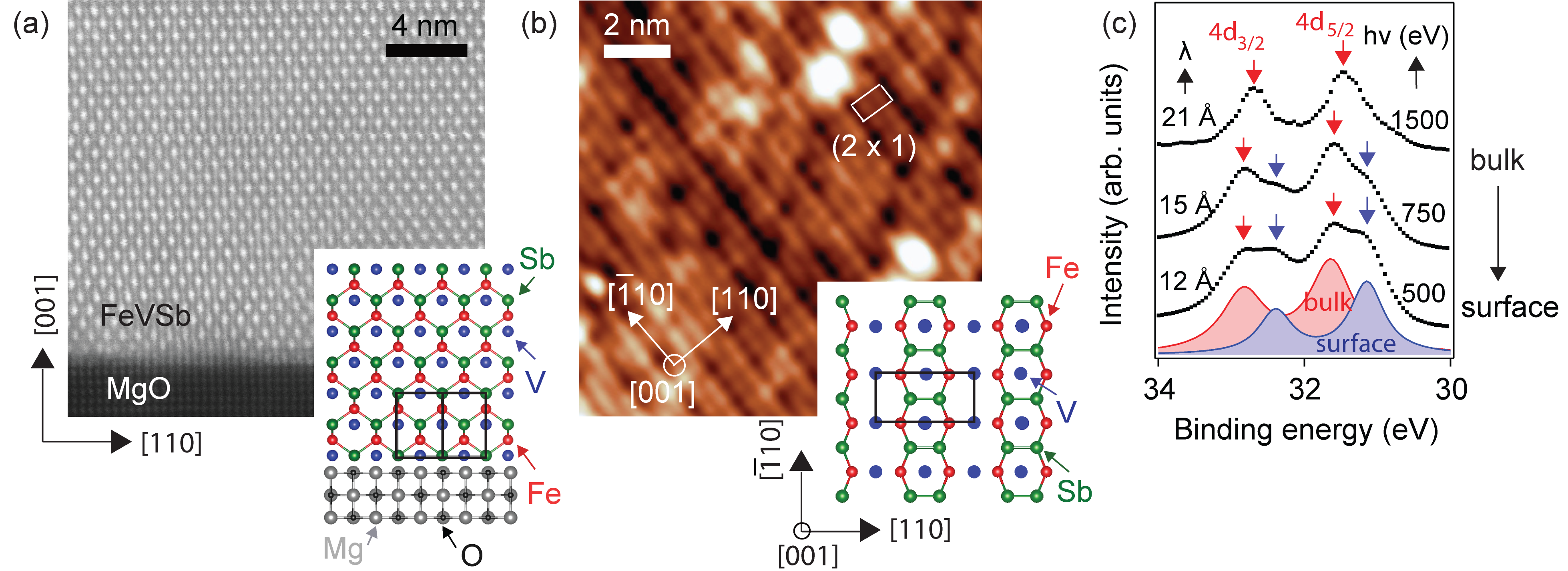
An overview of the bulk and surface structure of our FeVSb/MgO (001) films is shown in Fig. 1. The Z-contrast high angle annular dark field scanning transmission electron microscopy (HAADF-STEM) image in Fig. 1 (a) confirms an epitaxial FeVSb film on MgO with a 45 degree rotated cube-on-cube relationship, i.e. FeVSb MgO . Empty states scanning tunneling microscopy (STM, Fig. 1 (b)) images reveal a surface reconstruction, similar to what has been observed for other half Heusler (001) surfaces Kawasaki et al. (2018); Patel et al. (2016); Bach et al. (2003); Turban et al. (2002). To understand the origin of this surface reconstruction, we performed photon energy-dependent photoemission spectroscopy measurements at beamline 29-ID of the Advanced Photon Source (Fig. 1 (c). We find that with decreasing photon energy (increasing surface sensitivity), the Sb core level shows a secondary component with decreased binding energy that is localized to the surface. We attribute this secondary component to surface Sb-Sb dimerization Kawasaki et al. (2018). A proposed model of the surface atomic structure is shown in Fig. 1(b inset), characterized by Sb-Sb dimerization. Some concentration of surface V vacancies is expected based on surface charge neutrality Kawasaki et al. (2018); however, quantifying this effect is beyond the scope of the current study. Such vacancies are localized the surface and are expected to have negligible affect on the bulk properties. Further TEM, STM, and photoemission measurement details are found in the Supplemental Information.
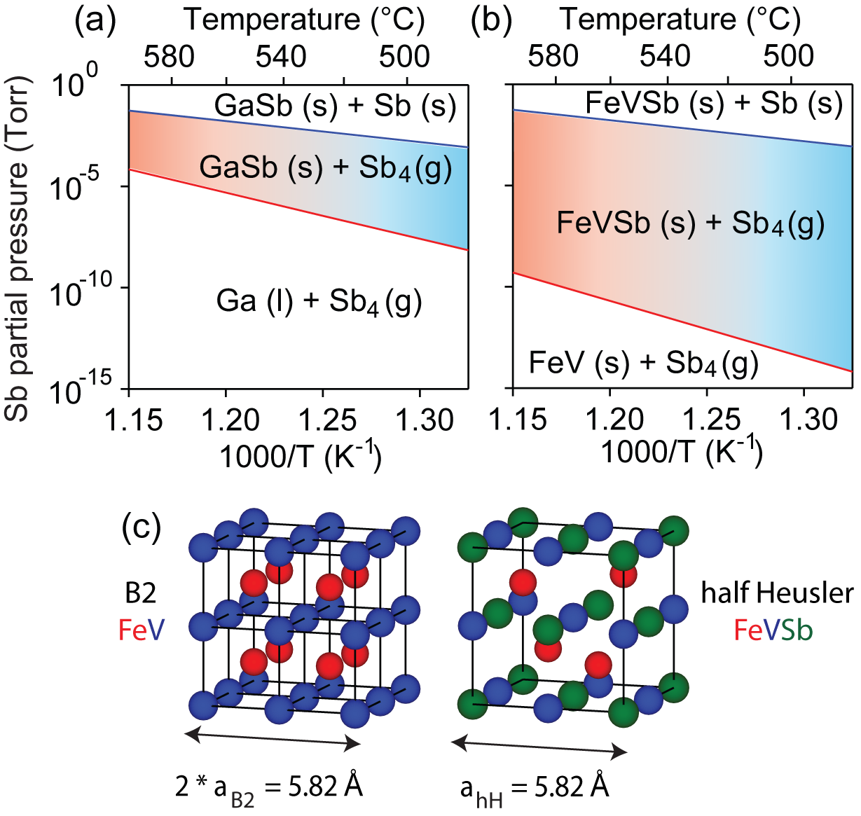
We first establish the thermodynamic basis for semi adsorption-controlled growth of FeVSb, in which the Sb stoichiometry is self-limiting. Fig. 2 compares the Ellingham diagram for FeVSb with that of GaSb, a III-V semiconductor that is routinely grown by adsorption-control. The common upper bound (blue curves), represents the change in Gibbs free energy for sublimation of antimony Sb(s) Sb4(g), as obtained from tabulated thermodynamic data Barin (1995). For temperature and Sb partial pressure combinations above this curve, solid antimony is expected to precipitate on the surface of the film. Below this curve, excess antimony is not expected to incorporate into the film, and instead escape into the vapor. The lower curves (red) represent the decomposition reactions GaSb(s) Ga(l) + Sb4(g) [Fig. 2(a)] and FeVSb(s) FeV(s) + Sb4(g) [Fig. 2(b)], respectively. The GaSb curve is obtained from completely from tabulated thermodynamic data Barin (1995). The FeVSb curve is calculated by combining density functional theory (DFT) calculations for FeVSb and FeV with tabulated thermodynamic data for Sb sublimation (see Supplemental Information). For temperature and Sb partial pressure combinations below these curves, FeVSb and GaSb are expected to decompose into their binary and elemental constituents, respectively. The regions bounded by the FeVSb (GaSb) decomposition and Sb sublimation curves define the expected growth windows for FeVSb and GaSb, respectively. Here, solid FeVSb or GaSb form with the stoichiometric composition of Sb, while the excess Sb escapes into the vapor. Based on these thermodynamic calculations, we expect that compared to GaSb, FeVSb should be stable at higher growth temperatures and lower Sb partial pressures. Few percent changes in the Fe/V stoichiometry produce minimal changes to the expected Ellingham diagram (Supplemental Fig. 1).
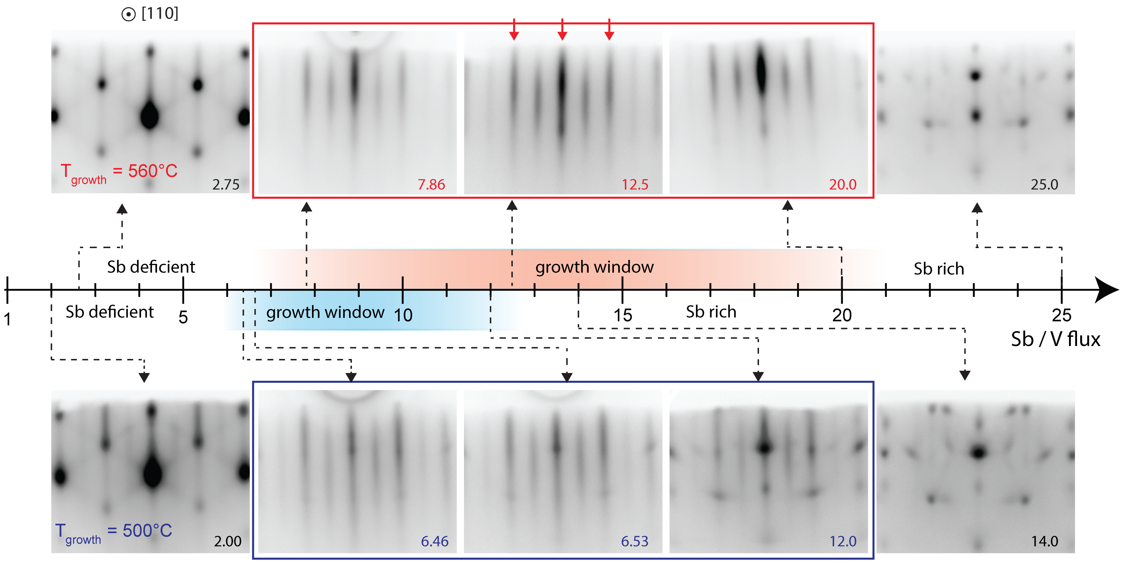
We now experimentally map the bounds of the FeVSb semi adsorption-controlled window. Fig. 3 (bottom) shows the RHEED patterns for samples grown at fixed temperature of 500C, as a function of Sb/V atomic flux ratio. For Sb/V flux ratio less than 5, the RHEED patterns are spotty, indicative of three-dimensional island formation. Based on the ternary Fe-V-Sb phase diagram, we expect highly Sb-deficient conditions to correspond to an epitaxial coexistence of FeV (B2 structure, Å) and FeVSb (half Heusler structure, Å), where Romaka et al. (2012) (Fig. 2(c)). There exists a range of moderate Sb/V fluxes, from approximately 5 to 12, in which a streaky RHEED pattern is observed, indicating smooth crystalline surfaces with FeVSb in half Heusler structure. This range of moderate Sb/V fluxes defines the growth window. Above an Sb/V flux ratio of 12, we observe additional spots in the RHEED pattern, indicative of Sb islands forming on the surface. Similar trends are observed for growth at a higher temperature of 560C, in which the bounds of the window are shifted towards higher Sb/V flux ratio as shown in Fig. 3 (top).
We further quantify the growth window for half Heusler phase by bulk-sensitive X-ray diffraction. Fig. 4 shows scans (Cu ) for samples grown at 500C and at 560C. In all samples we observe only -type FeVSb reflections, corresponding to epitaxial FeVSb films. We focus on the samples grown at 500 C; samples grown at 560C show similar qualitative behavior. Starting from an Sb/V atomic flux ratio of 2.0, with increasing relative Sb flux the relative intensity of the and reflections increases, and there is a shift in the reflection towards higher angle, corresponding to a decrease in the out-of-plane lattice parameter. In this region, we attribute the changes in structure factor and lattice parameter to two possible microstructures: (1) a mixture of FeV (B2) and FeVSb (half Heusler) phases under very Sb-deficient conditions, and (2) Sb vacancies near stoichiometric conditions. Firstly, for extremely low Sb flux conditions, a mixture of FeV (cubic B2) and FeVSb (half Heusler) phases is expected from the ternary phase diagram, in which the two phases are epitaxial to one another (ahH ) Romaka et al. (2012). The B2 phase has a much smaller 001B2/002B2 structure factor ratio than the equivalent half Heusler 002hH/004hH. With increasing Sb flux, the relative volume fraction of half Heusler FeVSb to B2 FeV increases, consistent with the observed increase in the 002/004 intensity ratio (Supplemental Fig. 3). Secondly, for Sb fluxes near stoichiometry, Sb vacancies may be present. Our structure factor calculations show that Sb vacancies in the half Heusler structure decrease the 002/004 and 006/004 structure factor ratio (Supplemental), consistent with the measured trends.
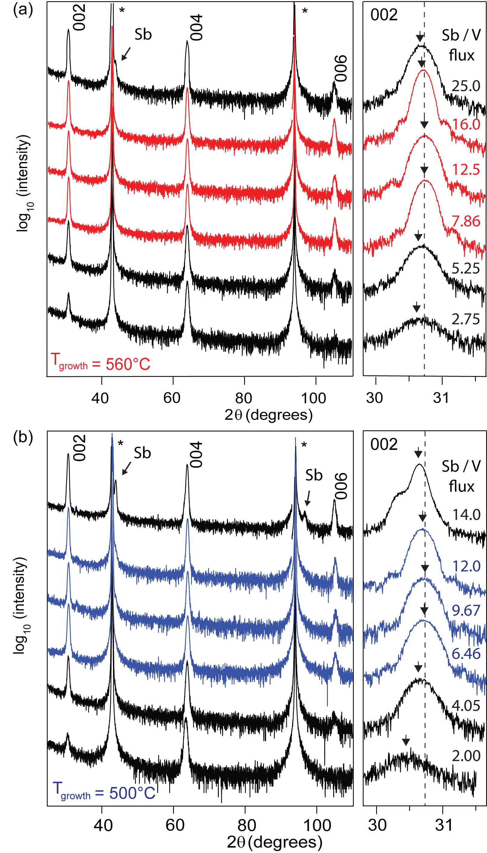
Over a wide range of intermediate Sb/V flux ratios, from approximately 6 to 12, both the relative intensities of the and reflections and the peak position of the reflection are constant. This broad range of of Sb/V defines the growth window, and the extracted lattice parameters from the and reflections are shown in Fig. 5(a). Here the lattice parameter for films within the window plateaus to a value of 5.82 Å, in good agreement with previously reported lattice constant of 5.826 Å for bulk samples Jodin et al. (2004). We attribute variations in the lattice parameter to variations in Fe/V composition, which in the present study vary by no more than 5 percent. Samples within this window show Kiessig fringes around the reflections (Fig. 4), indicative of smooth interfaces. Within this window, the Sb stoichiometry plateaus to a constant Sb/V=1.0, as measured by energy dispersive x-ray spectroscopy (EDS) that we calibrate in absolute scale to Rutherford Backscattering Spectrometry (RBS) measurements on a few select samples (Fig. 5(a), see Supplemental Information for measurement details and analysis methods).
For Sb/V flux greater than 12, we observe precipitation of a secondary phase in XRD (Fig. 4) and an increase in the out-of-plane lattice parameter (Fig. 5(a)). This defines the Sb-rich bound of the window. We find that the Sb-rich bound observed by XRD (Sb/V , Fig. 4) is higher than the bound defined by the onset of spottiness in the RHEED pattern (Sb/V , Fig. 3). We attribute this discrepancy to Sb precipitates localized to the surface, which can be detected by surface-sensitive RHEED but are not detected by bulk-sensitive X-ray diffraction.
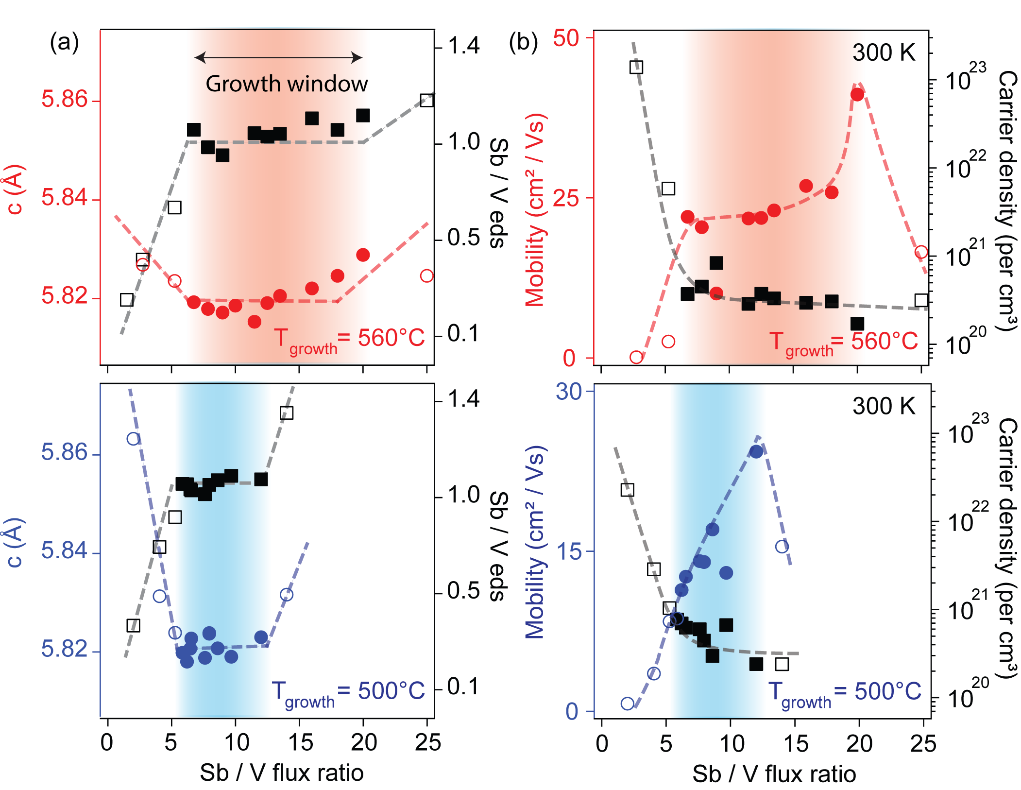
Fig. 5(b) shows the room temperature Hall electron mobility and density for samples grown at 500 and 560C. These measurements were performed using a Quantum Design Physical Properties Measurement System (PPMS) in a Van der Pauw geometry using annealed indium contacts. At low fields (H 0.7 T) the Hall resistance (Rxy) for some samples showed slight nonlinearities (Supplemental Fig. 5), which we attribute to ferromagnetic impurities that arise from slight Fe-nonstoichiometry. We extract the carrier density by fitting a single band model to the high field ( 2 T) regime, where all samples showed linear Rxy vs H. Starting from Sb-deficient conditions, we find that a sharp increase in mobility and decrease in carrier density as the Sb flux is increased into the growth window. Within the growth window, the carrier mobility increases with Sb/V flux and peaks at the Sb-rich bound of the structural growth window. This behavior suggests that Sb vacancies may be a low formation energy defect. While Sb vacancies are not readily detected by diffraction or composition measurements, they are expected to strongly contribute to carrier scattering.
Films grown at a higher temperature of 560C reach a higher peak mobility than films grown at 500C, which we attribute to increased atomic site ordering at higher growth temperature. The maximum mobility of 41 cm2/Vs at 300 K for FeVSb films grown inside a growth window is comparable to previously reported mobilities of epitaxial half Heusler films grown on MgO (001), but is smaller than the highest mobilities reported for films grown on III-V substrates such as InP (001) Patel et al. (2016); Kawasaki et al. (2013, 2014). We attribute the reduced mobility to antiphase domains that form as a result of growing a (001)-oriented half Heusler film (2-fold rotational symmetry) on a rocksalt MgO (001) substrate (4-fold rotation). Growth on a 2-fold surface of a (001)-oriented III-V surface is expected to yield higher mobility films Kawasaki et al. (2014).
Supplemental Fig. 6 shows the temperature dependence of the resistivity, mobility and carrier density of two 560C films, one grown in the middle (Sb/V flux 11.5) and the other at the Sb rich bound (Sb/V flux 20.0) of the structural growth window. For both samples, the electron density and resistivity show a weak temperature dependence, and the magnitude of the electron density of cm-3 is consistent with degenerate doping. We attribute this doping to antiphase domains induced by the 4-fold MgO (001) substrate and to a few percent deviation in the Fe/V stoichiometry, which is not self-limited. The mobilities increase with decreasing temperatures as expected with acoustic phonon freeze out at low temperatures. Further measurements are required to quantify and identify the defect-induced scattering mechanisms for films grown in the middle of the structural window versus the mobility-optimized films grown at near the Sb-rich bound of the structural window.
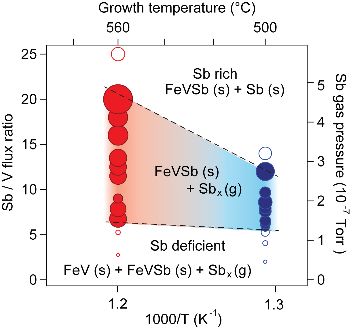
Our experimental phase diagram for semi adsorption-controlled growth is summarized in Fig. 6. Here the open circles represent films outside the growth window, filled circles represent films inside the growth window, and the size of the circles scales with the magnitude of the electron mobility. To facilitate comparisons with our Ellingham diagram prediction (Fig. 2), we estimate the Sb partial pressure using the kinetic theory of gases Farrow (1995), where (Fig. 6 right axis). Here is the Sb atomic flux, is the Boltzmann constant, C is the temperature of the Sb vapor, and amu is the mass of the Sb vapor species. The Sb vapor is assumed to be atomic Sb1 for approximation purposes, the true flux is a mixture of Sb1 and Sb2. We find that our experimental window is much narrower than the thermodynamic prediction: whereas the experimental window is centered around a Sb partial pressure of order Torr and spans a factor of 2.5 to 5 (Fig. 5(c)), the thermodynamic prediction spans several decades (Fig. 2(b)). We attribute this discrepancy to growth kinetics, which are not captured in the Ellingham diagram. Similar discrepancies are observed for other adsorption-controlled systems, such as GaSb. For GaSb the experimental Sb/Ga atomic flux window at C spans approximately a factor of ten Turner et al. (1993); Ivanov et al. (1993); Yano et al. (1978), much smaller than the several decade wide prediction from the Ellingham diagram (Fig. 2(a)). A more complete view of the growth window requires the includion of kinetics, which has recently been applied to the MBE growth of several transition metal oxides Smith et al. (2017).
In summary, we have established the thermodynamic basis and experimentally mapped the semi adsorption-controlled growth window for half Heusler FeVSb films, in which the Sb stoichiometry is self-limiting. Similar Sb adsorption-controlled windows are expected for CoTiSb, LuPtSb, and NiMnSb, which have also been grown previously by MBE with excess Sb fluxes Logan et al. (2016); Kawasaki et al. (2018); Bach et al. (2003), but whose growth window bounds have yet to be quantified. It remains an outstanding challenge to control the Fe/V stoichiometry, which is not self-limited when using atomic Fe and V fluxes from effusion cells. Recent demonstrations MBE-grown LiZnSb, in which all three atomic species are volatile, suggest that it may be possible to control the full stoichiometry of a ternary Heusler compound Du et al. (2020). However, for transition metal based Heuslers such as FeVSb, control of the transition metal ratio may require replacing one or both of the elemental transition metal sources with a volatile metalorganic precursor.
I Acknowledgments
We thank Fanny Rodolakis and Jessica L. McChesney for technical support during synchrotron photoemission measurements. This work was supported by the CAREER program of the National Science Foundation (DMR-1752797) and by the SEED program of the Wisconsin Materials Research Science and Engineering Center, an NSF funded center (DMR-1720415). Ryan Jacobs and Dane Morgan were supported by the Department of Energy (DOE) award number DE-SC0020419. We gratefully acknowledge the use of X-ray diffraction and electron microscopy facilities supported by the NSF through the University of Wisconsin Materials Research Science and Engineering Center under Grant No. DMR-1720415. This research used resources of the Advanced Photon Source, a U.S. Department of Energy (DOE) Office of Science User Facility operated for the DOE Office of Science by Argonne National Laboratory under Contract No. DE-AC02-06CH11357; additional support by National Science Foundation under Grant no. DMR-0703406. We thank Professor Song Jin for the use of PPMS facilities. We thank Mark Mangus (Eyring Materials Center, Arizona State University) and Greg Haugstad (Characterization Facility, University of Minnesota) for performing RBS measurements.
References
- Störmer et al. (1981) H. Störmer, A. Pinczuk, A. Gossard, and W. Wiegmann, Applied Physics Letters 38, 691 (1981).
- Tsui et al. (1982) D. C. Tsui, H. L. Stormer, and A. C. Gossard, Phys. Rev. Lett. 48, 1559 (1982).
- Tsao (2012) J. Y. Tsao, Materials fundamentals of molecular beam epitaxy (Academic Press, 2012).
- Cho and Arthur (1975) A. Cho and J. Arthur, Progress in Solid State Chemistry 10, 157 (1975), ISSN 0079-6786.
- Pfeiffer et al. (1989) L. Pfeiffer, K. West, H. Stormer, and K. Baldwin, Applied Physics Letters 55, 1888 (1989).
- Dingle et al. (1978) R. Dingle, H. Störmer, A. Gossard, and W. Wiegmann, Applied Physics Letters 33, 665 (1978).
- Klitzing et al. (1980) K. v. Klitzing, G. Dorda, and M. Pepper, Physical Review Letters 45, 494 (1980).
- Awano et al. (1989) Y. Awano, M. Kosugi, S. Kuroda, T. Mimura, and M. Abe, in Proceedings., IEEE/Cornell Conference on Advanced Concepts in High Speed Semiconductor Devices and Circuits, (IEEE, 1989), pp. 46–55.
- Ihlefeld et al. (2007) J. Ihlefeld, A. Kumar, V. Gopalan, D. G. Schlom, Y. Chen, X. Pan, T. Heeg, J. Schubert, X. Ke, P. Schiffer, et al., Applied Physics Letters 91, 071922 (2007).
- Paik et al. (2017) H. Paik, Z. Chen, E. Lochocki, A. Seidner H, A. Verma, N. Tanen, J. Park, M. Uchida, S. Shang, B.-C. Zhou, et al., APL Materials 5, 116107 (2017).
- Prakash et al. (2017) A. Prakash, P. Xu, X. Wu, G. Haugstad, X. Wang, and B. Jalan, Journal of Materials Chemistry C 5, 5730 (2017).
- Jalan et al. (2009) B. Jalan, P. Moetakef, and S. Stemmer, Applied Physics Letters 95, 032906 (2009).
- Brahlek et al. (2015) M. Brahlek, L. Zhang, C. Eaton, H.-T. Zhang, and R. Engel-Herbert, Applied Physics Letters 107, 143108 (2015).
- Graf et al. (2011) T. Graf, C. Felser, and S. S. Parkin, Progress in solid state chemistry 39, 1 (2011).
- Palmstrøm (2016) C. J. Palmstrøm, Progress in Crystal Growth and Characterization of Materials 62, 371 (2016).
- Yonggang et al. (2017) G. Y. Yonggang, X. Zhang, and A. Zunger, Physical Review B 95, 085201 (2017).
- Picozzi and Freeman (2007) S. Picozzi and A. J. Freeman, Journal of Physics: Condensed Matter 19, 315215 (2007).
- Picozzi et al. (2004) S. Picozzi, A. Continenza, and A. J. Freeman, Physical Review B 69, 094423 (2004).
- Öğüt and Rabe (1995) S. Öğüt and K. M. Rabe, Physical Review B 51, 10443 (1995).
- Larson et al. (2000) P. Larson, S. Mahanti, and M. Kanatzidis, Physical Review B 62, 12754 (2000).
- Kawasaki (2019) J. K. Kawasaki, APL Materials 7, 080907 (2019).
- Kawasaki et al. (2018) J. K. Kawasaki, A. Sharan, L. I. Johansson, M. Hjort, R. Timm, B. Thiagarajan, B. D. Schultz, A. Mikkelsen, A. Janotti, and C. J. Palmstrøm, Science advances 4, eaar5832 (2018).
- Kawasaki et al. (2014) J. K. Kawasaki, L. I. M. Johansson, B. D. Schultz, and C. J. Palmstrøm, Applied Physics Letters 104, 022109 (2014).
- Bach et al. (2003) P. Bach, A. Bader, C. Rüster, C. Gould, C. Becker, G. Schmidt, L. Molenkamp, W. Weigand, C. Kumpf, E. Umbach, et al., Applied physics letters 83, 521 (2003).
- Turban et al. (2002) P. Turban, S. Andrieu, B. Kierren, E. Snoeck, C. Teodorescu, and A. Traverse, Physical Review B 65, 134417 (2002).
- Patel et al. (2014) S. J. Patel, J. K. Kawasaki, J. Logan, B. D. Schultz, J. Adell, B. Thiagarajan, A. Mikkelsen, and C. J. Palmstrøm, Applied Physics Letters 104, 201603 (2014).
- Du et al. (2019) D. Du, A. Lim, C. Zhang, P. J. Strohbeen, E. H. Shourov, F. Rodolakis, J. L. McChesney, P. Voyles, D. C. Fredrickson, and J. K. Kawasaki, APL Materials 7, 121107 (2019).
- Strohbeen et al. (2019) P. J. Strohbeen, D. Du, C. Zhang, E. H. Shourov, F. Rodolakis, J. L. McChesney, P. M. Voyles, and J. K. Kawasaki, Physical Review Materials 3, 024201 (2019).
- Young et al. (2000) D. Young, P. Khalifah, R. J. Cava, and A. Ramirez, Journal of Applied Physics 87, 317 (2000).
- Seah and Dench (1979) M. P. Seah and W. Dench, Surface and interface analysis 1, 2 (1979).
- Patel et al. (2016) S. J. Patel, J. A. Logan, S. D. Harrington, B. D. Schultz, and C. J. Palmstrøm, Journal of Crystal Growth 436, 145 (2016).
- Barin (1995) I. Barin, Thermochemical Data of Pure Substances, vol. 2 (VCH, 1995), 3rd ed.
- Romaka et al. (2012) V. V. Romaka, L. Romaka, Y. Stadnyk, V. Gvozdetskii, R. Gladyshevskii, N. Skryabina, N. Melnychenko, V. Hlukhyy, and T. Faessler, European Journal of Inorganic Chemistry 2012, 2588 (2012).
- Jodin et al. (2004) L. Jodin, J. Tobola, P. Pecheur, H. Scherrer, and S. Kaprzyk, Phys. Rev. B 70, 184207 (2004).
- Kawasaki et al. (2013) J. K. Kawasaki, T. Neulinger, R. Timm, M. Hjort, A. A. Zakharov, A. Mikkelsen, B. D. Schultz, and C. J. Palmstrøm, Journal of Vacuum Science & Technology B 31, 04D106 (2013).
- Farrow (1995) R. F. Farrow, Molecular beam epitaxy: applications to key materials (Elsevier, 1995).
- Turner et al. (1993) G. Turner, S. Eglash, and A. J. Strauss, Journal of Vacuum Science & Technology B: Microelectronics and Nanometer Structures Processing, Measurement, and Phenomena 11, 864 (1993).
- Ivanov et al. (1993) S. Ivanov, P. Altukhov, T. Argunova, A. Bakun, A. Budza, V. Chaldyshev, Y. A. Kovalenko, P. Kop’ev, R. Kutt, B. Y. Meltser, et al., Semiconductor science and technology 8, 347 (1993).
- Yano et al. (1978) M. Yano, Y. Suzuki, T. Ishii, Y. Matsushima, and M. Kimata, Japanese Journal of Applied Physics 17, 2091 (1978).
- Smith et al. (2017) E. H. Smith, J. F. Ihlefeld, C. A. Heikes, H. Paik, Y. Nie, C. Adamo, T. Heeg, Z.-K. Liu, and D. G. Schlom, Physical Review Materials 1, 023403 (2017).
- Logan et al. (2016) J. A. Logan, S. Patel, S. D. Harrington, C. Polley, B. D. Schultz, T. Balasubramanian, A. Janotti, A. Mikkelsen, and C. J. Palmstrøm, Nature communications 7, 11993 (2016).
- Du et al. (2020) D. Du, P. J. Strohbeen, H. Paik, C. Zhang, K. T. Genser, K. M. Rabe, P. M. Voyles, D. G. Schlom, and J. K. Kawasaki, Journal of Vacuum Science & Technology B 38, 022208 (2020), URL https://doi.org/10.1116/1.5145217.