Hypersensitive tunable Josephson escape sensor for gigahertz astronomy
Abstract
Single-photon detectors and bolometers represent the bridge between different topics in science, such as quantum computation, astronomy, particle physics and biology. Nowadays, superconducting bolometers and calorimeters are the most sensitive detectors in the THz and sub-THz bands. Here, we propose and demonstrate a Josephson escape sensor (JES) that could find natural application in astrophysics. The JES is composed of a fully superconducting one-dimensional Josephson junction, whose resistance versus temperature characteristics can be precisely controlled by a bias current. Therefore, differently from the traditional superconducting detectors, the JES sensitivity and working temperature can be in situ simply and finely tuned depending on the application requirements. Interestingly, a JES bolometer is expected to show an intrinsic thermal fluctuation noise equivalent power () of the order of W/Hz1/2, while a JES calorimeter could provide a frequency resolution of about 2 GHz, as deduced from the experimental data. In addition, the sensor can operate at the critical temperature, i.e., working as a conventional transition edge sensor (TES), with a W/Hz1/2 and a frequency resolution GHz.
I Introduction
Sensitive photon detection in the gigahertz band constitutes the cornerstone to study different phenomena in astronomy Rowan2009 , such as radio burst sources Marcote2020 , galaxy formation Tabatabaei2017 , cosmic microwave background Sironi1999 , axions Capparelli2016 ; Irastorza2018 , comets Falchi1988 , gigahertz-peaked spectrum radio sources Odea1998 and supermassive black holes Issaoun2019 . Nowadays, state of the art detectors for astrophysics are mainly based on transition edge sensors Irwin1995 ; Irwin2006 ; Khosropanah2010 and kinetic inductance detectors Day2003 ; Visser2014 ; Monfardini2016 . Overall, most sensible nanobolometers so far are superconducting detectors Morgan2018 showing a noise-equivalent power (NEP) as low as W/Hz1/2 Kokkoniemi2019 . Yet, fast thermometry at the nanoscale was demonstrated as well with Josephson junctions through switching current measurements Zgirski2018 ; Wang2018 . In general, detection performance are set by the fabrication process and limited by used materials.
In this work, we conceive and demonstrate a tunable Josephson escape sensor (JES) based on the precise current control of the temperature dependence of a fully superconducting one-dimensional nanowire Josephson junction. The JES might be at the core of future hypersensitive in situ-tunable bolometers or single-photon detectors working in the gigahertz regime. Operated as a bolometer the JES points to a thermal fluctuation noise (TFN) NEP W/Hz1/2, which as a calorimeter bounds the frequency resolution above GHz, and resolving power below at GHz, as deduced from the experimental data.
Beyond the obvious applications in advanced ground-based Ade2019 and space Adams2020 telescopes for gigahertz astronomy, the JES might represent a breakthrough in several fields of quantum technologies ranging from sub-THz communications Federici2010 and quantum computing Obrien2007 to cryptography Gisin2002 and quantum key distribution Tittel2019 .
II GHz astrophysics and JES operation principle
Many features of the universe are hidden in infrared and microwave faint signals Rowan2009 . In particular, the study of cosmic microwave background polarization Sironi1999 ; Seljak1997 and galaxy expansion Tabatabaei2017 benefits from ultrasensitive gigahertz bolometers, while the existence of axion-like-particles Irastorza2018 ; Capparelli2016 might be proven through the revelation of microwave single-photons (see Fig. 1-a).
To improve photon detection sensitivity, novel superconducting sensors have been developed by miniaturizing the active region Karasik2007 ; Wei2008 , and drastically lowering their operation temperature via the Josephson coupling in complex nanostructures Kokkoniemi2019 ; Chen2011 ; Nararajan2012 ; Karimi2020 ; Virtanen2018 ; Giazotto2008 ; Kuzmin2019 ; Govenius2016 . Their properties are thus defined during the fabrication process and can not be tuned during the operation. In analogy to the widespread transition edge sensor (TES), the JES exploits the change of resistance of a superconductor when transitioning to the dissipative state: either the absorption of radiation or the change of temperature Zgirski2018 ; Wang2018 trigger the passage from the superconducting to the normal regime yielding a sizable signal from the sensor. In contrast to TESs, the JES benefits from the possibility to finely tune in situ its working temperature and sensitivity.
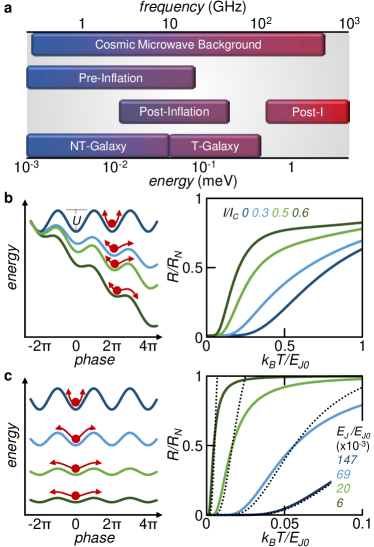
The JES operation principle is based on a fully superconducting one-dimensional (1D) Josephson junction (JJ), i.e., two superconducting leads coupled by a superconducting nanowire with lateral dimensions smaller than its coherence length (). The transition to the dissipative state can be understood to be due to phase-slips, qualitatively similar to the tilted washboard potential model (WP) of JJs, where a phase particle moves in the WP under action of friction forces Barone1982 ; Tinkham1996 . The effective WP profile strongly depends on both bias current () through the junction and Josephson energy () Bezryadin2012 [see left panels of Figs. 1(b)-1(c)]. In particular, for a 1D nanowire JJ the escape barrier can be written as Bezryadin2012
| (1) |
where , Wb is the flux quantum, and is the JJ critical current. Equation 7 shows that the phase particle escape from a potential minimum (and, therefore, the corresponding transition of the junction to the dissipative state) can be finely controlled either by rising or by suppressing .
Thanks to the exploitation of a 1D JJ, the JES benefits from a two-fold advantage. On the one hand, transverse dimensions smaller than ensure a constant superconducting wave function along the wire cross section leading to uniform superconducting properties. On the other hand, a nanowire width () much smaller than the London penetration depth () guarantees the supercurrent density in the JJ to be homogeneous when current-biasing the JES, and a uniform penetration of the film by an external magnetic field.
For comparison, in a sufficiently shunted overdamped limit, we can evaluate the resistance () versus temperature () characteristics of a JJ for different values of and by calculating the current derivative of the voltage drop Ivanchenko1969
| (2) |
where is the JJ zero-temperature critical current, is the modified Bessel function with imaginary argument , and . The details of the theoretical model are in the Supplemental Material SU .
Specifically, an increase of leads to a sizable lowering of the resistive transition temperature accompanied by its narrowing, as shown in the right panel of Fig. 1(b) for (where is the zero-temperature Josephson energy). Similarly, the transition temperature can be reduced by decreasing , but its width results wider than in the presence of a sizable bias current flowing through the nanowire [see the right panel of Fig. 1(c)]. In fact, the black dotted curves are calculated for by varying in order to have the same transition temperature () given by the reduction of Josephson energy. The temperature response of originating from the biasing current yields transitions which are sharper than those obtained by simply reducing .
Note that can be suppressed, for instance, by applying an external magnetic field (). However, the use of can be detrimental for several applications, since it typically broadens the superconducting transition Zant1992 . As we shall show, tuning the nanowire JJ through current injection will prove to be an excellent strategy to achieve near-to-ideal nanosensors with ultimate performance.
III JES structure and basic characterization
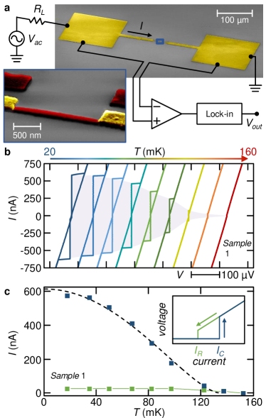
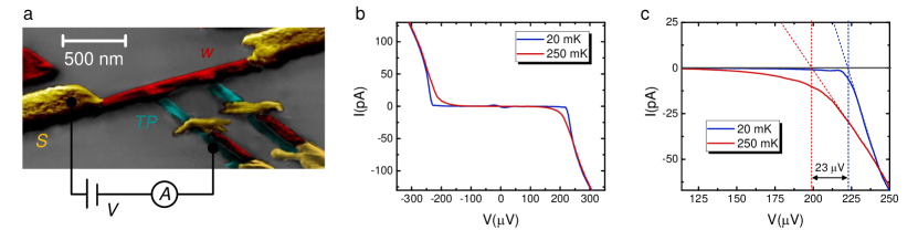
The realization of a typical JES is shown in the pseudo-color scanning electron micrograph displayed in Fig. 2(a). The JESs were fabricated by electron-beam lithography and two angles shadow-mask electron-beam evaporation of metals onto an oxidized silicon wafer through a suspended resist mask. The 1D sensor active region consists of a bilayer of Al ( nm) and Cu ( nm) evaporated at an angle of 0∘. The total volume of the sensor active region is m-3, with m-3 and m-3. The lateral 40-nm-thick Al banks were then evaporated at an angle of 40∘.
All measurements were performed in a filtered He3-He4 dry dilution refrigerator at different bath temperatures in the range mK. The resistance vs temperature characteristics of the JES and of the Al banks were obtained by conventional four-wire low-frequency lock-in technique at Hz. To this end, AC excitation currents with typical root mean square amplitudes nA were imposed through the device. The current was generated by applying an AC voltage bias () to a load resistor of impedance () much larger than the sample resistance ( k). The critical temperature of the Al banks was measured with the same set-up. The vs characteristics of the nanowires were obtained by applying a low-noise DC biasing current, while the voltage drop was measured via a room-temperature battery-powered differential preamplifier.
Josephson transport in the nanosensor is highlighted by the DC current () vs voltage () characteristics shown in Fig. 2(b) for bath temperatures () ranging from 20 mK to 160 mK. The wire normal-state resistance is , and the typical heating-induced hysteretic behavior of the curves is observed Courtois2008 . On the one hand, the critical current obtains a maximum nA at mK [see Fig. 2(c)], and monotonically decreases with following the prediction of Bardeen Bardeen1962 (see Appendix A for details). On the other hand, the retrapping current ( nA) is constant in the whole temperature range.
As stated, the JES working principle is based on a 1D nanowire JJ. Indeed, the coherence length ( nm) and the London penetration depth ( nm) of the nanowire are much larger than the wire width ( nm) and total film thickness ( nm) thereby providing the frame of a 1D junction (see Appendix A). Yet, the nanowire length () reduces the influence of the superconducting proximity effect arising from the clean contact with the lateral Al leads Tinkham1996 . We also note that the maximum magnetic field created by the critical current flow, T, is negligibly small compared to the out-of-plane critical magnetic field of the wire ( mT) thus implying a vanishing effect on the JES.
IV Current modulation of the R vs T characteristics
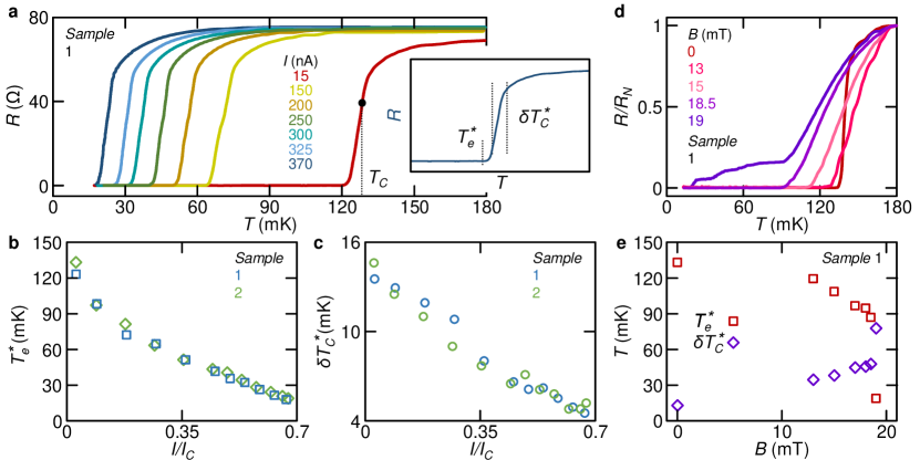
We investigated the behavior of the JES by recording the resistance versus temperature characteristics for several amplitudes of low-frequency AC bias current [see Fig. 3(a)]. The characteristics monotonically shift towards low temperatures by increasing , almost preserving the same shape up to the largest current amplitude. In particular, was varied between and of . Note that although the transition curves shift towards low by increasing , the nanowire electronic temperature in the middle of the transition under current injection is not expected to coincide anymore with the bath temperature . Indeed, when transitioning to the normal state, electrons in the nanowire are Joule overheated with respect to by the bias current (with final ), thus preventing the operation of the nanosensor as a conventional TES biased at those low bath temperatures, without additional shunting. By contrast, when operated in the dissipationless regime, i.e., as an escape sensor, coincides with .
From the vs curves we can specify a current-dependent temperature related to the resistive transition, i.e., the escape temperature []. The latter is the maximum value of providing a zero nanowire resistance (see the inset of Fig. 3(a) and Appendix A). The characteristics for two JES samples are shown in Fig. 3(b). In particular, is monotonically reduced by increasing with a minimum value mK for nA corresponding to of the nanowire intrinsic critical temperature, mK. Moreover, the transition width () narrows by increasing [see Fig. 3(c)]. In particular, is suppressed by a factor of at the largest current amplitude, mirroring the expected changes in the switching as shown in Fig. 1(b).
In addition, to prove the complementary tuning of the WP through the suppression of (see Eq. 7), we applied a perpendicular-to-plane magnetic field. The resulting shape of the corresponding transition degrades dramatically in the presence of [see Fig. 3(d)]. n particular, the vs characteristics appear to be scarcely tunable, while the onset of the transition is almost unaffected. The extreme broadening of the superconducting to dissipative state transition can be explained in terms of flux penetration in the nanowire and in the aluminum banks, since our nanowires are thinner than the London penetration depth for magnetic field (see Appendix A for details). shows a stark variation at values of , and is joined to the outbreak of the transition width, as displayed in Fig. 3(e). The above results in a finite magnetic field validate therefore the bias current as an ideal tool to control the JES properties.
V Performance of JES-based bolometers and calorimeters
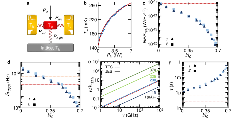
Insight into the behavior of the JES can be gained by considering the predominant heat exchange mechanisms occurring in the nanodevice, as schematically depicted in the thermal model of Fig. 4(a). The absorption of external incident radiation () leads to the increase of the nanowire electronic temperature . Yet, the two lateral superconducting Al leads (residing at bath temperature ) serve as Andreev mirrors Andreev1964 thereby suppressing heat out-diffusion () from the nanowire. As a consequence, the main thermal relaxation channel in the system stems from heat exchange with lattice phonons () residing at . For a normal metallic thin film, Irwin1995 ; Giazotto2006 , where is the nanowire volume, and is the electron-phonon coupling constant of the bilayer. was determined through energy-relaxation experiments Giazotto2006 by injecting a known power, and by measuring the resulting steady-state electron temperature established in an ad hoc fabricated identical wire kept above its critical temperature. Figure 4(b) shows the vs characteristic (blue dots) recorded at mK along with a fit to the data which allows to extract the electron-phonon coupling constant in the Al/Cu nanowire, Wm-3K-5 (see Supplemental Material SU ).
Yet, since the JES is operated in the superconducting state at , the latter can be substantially smaller than depending on the current amplitude. At sufficiently low temperature, the electron-phonon heat exchange in a superconductor is exponentially suppressed with respect to the normal state owing to the presence of the energy gap, i.e., Timofeev2009 , where eV is the pairing potential in the nanowire (see Supplemental Material for details). As we shall argue, the operation deeply in the superconducting state dramatically improves the JES key figures of merit for radiation detection.
In general, the performance of a bolometer can be quantified by the NEP that is the input power resolution per unit bandwidth. For the JES, the NEP is bounded by thermal fluctuations between the electron and phonon system in the nanowire Giazotto2006 . Other limitations to the resolution can arise from the switching measurement, which we assume is optimized to be sub-dominant. The thermal fluctuation noise (TFN)-limited NEPTFN can be extracted by substituting the measured parameters of the JES, such as vs. , characteristics, and , in the widespread and well known equations for superconducting radiation sensors Giazotto2006 (see also Supplemental Material SU ). The NEPTFN monotonically decreases by increasing the current amplitude, and turns out to be in-situ finely controlled by tuning [see Fig. 4(c)]. In particular, the JES points to noise values which are several orders of magnitude smaller than so far reported. Specifically, the best extracted NEPTFN obtains values as low as W/ for nA at mK. By contrast, in the normal state, i.e., when it is operated as a conventional TES, the sensor is expected to provide a much higher NEP W/, because the electron-phonon thermalisation in the active region is stronger.
In pulsed detection mode, a relevant figure of merit of a radiation sensor is represented by the frequency resolution (), i.e., the minimum detectable energy for an incident single photon (see Supplemental Material for details SU ). We here assume the JES measurement is performed accurately and sufficiently fast Zgirski2018 ; Wang2018 compared to the thermal relaxation time , and estimate the limitation from the TFN. Figure 4(d) emphasizes the strong dependence of on which displays variations over orders of magnitude. For , this limit can be as low as GHz at nA, and would enable single-photon sensing at unprecedented low energies. When operating the nanosensor as TES, is roughly two orders of magnitude larger, and obtains GHz. The limitation to single-photon sensing capability from TFN in our JES is highlighted by the resolving power (), calculated vs incident radiation frequency in Fig. 4(e). can reach at GHz, and at THz both for nA, whereas it can be at THz when operating the sensor as a TES. Since the power associated to 1 THz photons is lower than W and the power dissipated through the phonons at mK is about 6 fW [see Fig. 4(b)], the electronic temperature in the wire is always lower than . Therefore, we can exclude thermal diffusion through the aluminum banks Andreev1964 thus considering the active region fully thermally isolated from the electrodes.
We wish to finally comment onto the JES time constant (), which is one of the fundamental figures of merit for a radiation sensor. It is basically given by the ratio between the electron heat capacitance and the electron-phonon heat conductance in the nanowire Giazotto2006 , since heat conduction through the lateral Al electrodes is negligible in a JES. In pulsed detection mode determines the minimum speed of the read-out electronics (which has to be faster than ), and the minimum time separation for the independent detection of two photons. Figure 4(f) shows the expected JES time constant vs bias current , as deduced from the experimental data (see Supplemental Material for details). In particular, increases monotonically by increasing , and varies between s at low current amplitude and ms at nA. In general, when used at as a TES, the nanosensor can provide a much faster response than the JES in the whole bias current range ( ns) thanks to the higher operation temperature and electron-phonon thermal relaxation.
VI Conclusions
We have conceived and demonstrated an innovative hypersensitive superconducting radiation sensing element supplied with the capability of in-situ fine tuning its performances by a current bias. Our nanosensor has the potential to drive radiation detection in the gigahertz regime towards unexplored levels of sensitivity by lowering the thermal fluctuation limitation to NEP down to W/, with a corresponding limit in frequency resolution at GHz. The JES is expected to have significant impact in radio astronomy Rowan2009 ; Marcote2020 ; Tabatabaei2017 ; Sironi1999 ; Falchi1988 ; Issaoun2019 ; Adams2020 ; Ade2019 , space spectroscopy Odea1998 and dark matter search Capparelli2016 ; Irastorza2018 , since its working mechanism could allow, in principle, the immediate replacement of TESs in already existing experiments and telescopes. Furthermore, the JES could have countless applications in several fields of quantum technology where extrasensitive photon detection is a fundamental task, such as sub-terahertz communication Federici2010 , quantum computation Obrien2007 and quantum cryptography Gisin2002 ; Tittel2019 .
Acknowledgements
We acknowledge F. S. Bergeret, G. De Simoni, E. Strambini, A. Tartari, and G. Marchegiani for fruitful discussions. The authors acknowledge the European Union’s Horizon 2020 research and innovation programme under the grant No. 777222 ATTRACT (Project T-CONVERSE) and under grant agreement No. 800923-SUPERTED. The authors acknowledge CSN V of INFN under the technology innovation grant SIMP. The work of F.P. was partially supported by the Tuscany Government (Grant No. POR FSE 2014-2020) through the INFN-RT2 172800 project. The work of V.B. is partially funded by the European Union (Grant No. 777222 ATTRACT) through the T-CONVERSE project.
APPENDIX A: Device parameters
The temperature dependence of the critical current of the nanowire can be fitted through the phenomenological equation Bardeen1962 , where is the zero-temperature critical current. The fit provides nA and a critical temperature mK, which is good in agreement with the experimental value obtained from the resistance versus temperature characteristics.
The Al/Cu bilayer can be considered as an uniform superconductor, since it lies within the Cooper limit DeGennes1964 ; Kogan1982 . Here, we assume a transparent Al/Cu interface. Moreover, the aluminum layer respects nm (with the reduced Planck constant, m2s-1 is the diffusion constant of Al and eV its superconducting energy gap), while the copper film obeys to nm (with m2s-1 the copper diffusion constant and the temperature is chosen to the worst case scenario mK).
From the nanowire normal-state resistance ( ) we determined the superconducting coherence length in the active region nm, where is the electron charge, while J-1m-3 and J-1m-3 are the density of states at the Fermi level of aluminum and copper, respectively. As a consequence, the nanowire obeys to thus ensuring constant pairing potential along the out-of-plane axis. The superconducting energy gap of the bilayer, eV, has been determined by tunnel spectroscopy performed on ad hoc fabricated nominally identical wires equipped with Al tunnel probes. For further details, see Supplemental Material. The London penetration depth was determined as nm, where is the magnetic permeability of vacuum. The maximum magnetic field generated by the bias current at the wire surface reads T, where is the zero-temperature critical current, and is the total thickness of the JES active region. Finally, the critical temperature of the Al banks was K.
We would like to note that the energy gap expected for a non-superconducting Al/Cu bilayer would e eV, where m2s-1 is the wire diffusion coefficient and m is its length. This values is less than 1/4 of the measured gap. Therefore, the intrinsic superconductivity of the bilayer dominates.
The current-dependent escape temperature [] is defined as the maximum value of temperature providing , i.e., when the JES is in the dissipationless state.
References
- (1) M. Rowan-Robinson, Probing the Cold Universe, Science 325, 546-547 (2009).
- (2) B. Marcote, K. Nimmo, J. W. T. Hessels, S. P. Tendulkar, C. G. Bassa, Z. Paragi, A. Keimpema, M. Bhardwaj, R. Karuppusamy, V. M. Kaspi, et al. A repeating fast radio burst source localized to a nearby spiral galaxy, Nature 577, 190-194 (2020).
- (3) F. S. Tabatabaei, E. Schinnerer, M. Krause, G. Dumas, S. Meidt, A. Damas-Segovia, R. Beck, E. J. Murphy, D. D. Mulcahy, B. Groves, et. al. The Radio Spectral Energy Distribution and Star-formation Rate Calibration in Galaxies, ApJ 836, 185 (2017).
- (4) G. Sironi, The frequency spectrum of the Cosmic Microwave Background, New Astron. Rev. 43, 243-249 (1999).
- (5) L. M. Capparelli, G. Cavoto, J. Ferretti, F. Giazotto, A. D. Polosa, and P. Spagnolo, Axion-like particle searches with sub-THz photons, Phys. Dark Univ. 12, 37-44 (2016).
- (6) I. G. Irastorza, and J. Redondo, New experimental approaches in the search for axion-like particles, Prog. Part. Nucl. Phys. 102, 89 (2018).
- (7) A. Falchi, L. Gagliardi, F. Palagi, G. Tofani, and G: Comoretto, 10.7 GHz continuum observations of comet P/Halley (Springer, 1988).
- (8) C. P. O’Dea, The Compact Steep-Spectrum and Gigahertz Peaked-Spectrum Radio Sources, PASP 110, 493-532 (1998).
- (9) S. Issaoun, M. D. Johnson, L. Blackburn, C. D. Brinkerink, M. Mościbrodzka, A. Chael, C. Goddi, I. Martí-Vidal, J. Wagner, S. S. Doeleman, et. al. The Size, Shape, and Scattering of Sagittarius A* at 86 GHz: First VLBI with ALMA, ApJ 871, 30 (2019).
- (10) K. D. Irwin, An application of electrothermal feedback for high resolution cryogenic particle detection, Appl. Phys. Lett. 66, 1998-2000 (1995).
- (11) K. D. Irwin, Seeing with Superconductors, Sci. Am. 295, 86-94 (2006).
- (12) P. Khosropanah, B. Dirks, M. Parra-Borderías, M. Ridder, R. Hijmering, J. van der Kuur, L. Gottardi, M. Bruijn, M. Popescu, J. R. Gao, and H. Hoevers, Low noise transition edge sensor (TES) for the SAFARI Instrument on SPICA. in Proc. SPIE 7741, Millimeter, Submillimeter, and Far-Infrared Detectors and Instrumentation for Astronomy V, 77410L (2010).
- (13) P. K. Day, H. G. LeDuc, B. A. Mazin, A. Vayonakis, and J. Zmuldzinas, A broadband superconducting detector suitable for use in large arrays, Nature 425, 817-821 (2003).
- (14) P. J. Visser, J. J. A. Baselmans, J. Bueno, N. Llombart, and T. M. Klapwijk, Fluctuations in the electron system of a superconductor exposed to a photon flux. Nat. Comm. 5, 3130 (2014).
- (15) A. Monfardini, J. Baselmans, A. Benoit, A. Bideaud, O. Bourrion, A. Catalano, M. Calvo, A. D’Addabbo, S. Doyle, J. Goupy, H. Le Sueur, and J. Macias-Perez, Lumped element kinetic inductance detectors for space applications. in Proc. SPIE 9914, Millimeter, Submillimeter, and Far-Infrared Detectors and Instrumentation for Astronomy VIII, 99140N (2016).
- (16) K. Morgan, Hot science with cool sensors, Phys. Today 71, 28- 34 (2018).
- (17) R. Kokkoniemi, J. Govenius, V. Vesterinen, R. E. Lake, A. M. Gunyhó, K. Y. Tan, S. Simbierowicz, L. Grönberg, J. Lehtinen, M. Prunnila, J. Hassel, A. Lamminen, O.-P. Saira, and M. Möttönen, Nanobolometer with ultralow noise equivalent power, Commun Phys 2, 124 (2019).
- (18) M. Zgirski, M. Foltyn, A. Savin, K. Norowski, M. Meschke, and J. P. Pekola, Nanosecond Thermometry with Josephson Junctions, Phys. Rev. Applied 10, 044068 (2018).
- (19) L. B. Wang, O.-P. Saira, J. P. Pekola, Fast thermometry with a proximity Josephson junction Appl. Phys. Lett. 112, 013105 (2018).
- (20) P. Ade, et al., The Simons Observatory collaboration, The Simons Observatory: science goals and forecasts, JCAP02 2019, 056 (2019).
- (21) J. S. Adams, R. Baker, S. R. Bandler, N. Bastidon, M. E. Danowski, W. B. Doriese, M. E. Eckart, E. Figueroa-Feliciano, D. C. Goldfinger, S. N. T. Heine, G. C. Hilton, A. J. F. Hubbard, R. L. Kelley, C. A. Kilbourne, R. E. Manzagol-Harwood, D. McCammon, T. Okajima, F. S. Porter, C. D. Reintsema, P. Serlemitsos, S. J. Smith, J. N. Ullom, and P. Wikus, First Operation of TES Microcalorimeters in Space with the Micro-X Sounding Rocket, J Low Temp Phys 199, 1062–1071 (2020).
- (22) J. Federici, and. L. Moeller, Review of terahertz and subterahertz wireless communications, J. Appl. Phys. 107, 111101 (2010).
- (23) J. L. O’brien, Optical Quantum Computing, Science 318, 1567-1570 (2007).
- (24) N. Gisin, G. Ribordy, W. Tittel, and H. Zbiden, Quantum cryptography, Rev. Mod. Phys. 74, 145-195 (2002).
- (25) W. Tittel, Quantum key distribution breaking limits, Nat. Photonics 13, 310-311 (2019).
- (26) U. Seljak, and M. Zaldarriaga, Signature of gravity waves in the polarization of the microwave background, Phys. Rev. Lett. 78, 2054 (1997).
- (27) B. S. Karasik, D. Olaya, J. Wei, S. Pereverzev, M. E. Gershenson, J. H. Kawamura, W. R. McGrath, and A. V. Sergeev, Record-Low NEP in Hot-Electron Titanium Nanobolometers, IEEE Trans. Appl. Supercond. 17, 293-297 (2007).
- (28) J. Wei, D. Olaya, B. S. Karasik, S. V. Pereverzev, A. V. Sergeev, and M. E. Gershenson, Ultrasensitive hot-electron nanobolometers for terahertz astrophysics, Nat. Nanotech. 3, 496-500 (2008).
- (29) Y.-F. Chen, D. Hover, S. Sendelbach, L. Maurer, S. T. Merkel, E. J. Pritchett, F. K. Wilhelm, and R. McDermott, Microwave Photon Counter Based on Josephson Junctions, Phys. Rev. Lett. 107, 217401 (2011).
- (30) C. M. Natarajan, M. G. Tanner, and R, H. Hadfield, Superconducting nanowire single-photon detectors: physics and applications, Supercond. Sci. Technol. 25, 063001 (2012).
- (31) J. Govenius, R. E. Lake, K. Y. Tan, and M. Möttönen, Detection of Zeptojoule Microwave Pulses Using Electrothermal Feedback in Proximity-Induced Josephson Junctions, Phys. Rev. Lett. 117, 030802 (2016).
- (32) L. S. Kuzmin, A. L. Pankratov, A. V. Gordeeva, V. O. Zbrozhnek, V. A. Shamporov, L. S. Revin, A. V. Blagodaktin, S. Masi, and P. de Bernardis, Photon-noise-limited cold-electron bolometer based on strong electron self-cooling for high-performance cosmology missions, Commun Phys 2, 104 (2019).
- (33) B. Karimi, F. Brange, P. Samuelsson, and J. P. Pekola, Reaching the ultimate energy resolution of a quantum detector, Nat. Comm. 11, 367 (2020).
- (34) P. Virtanen, A. Ronzani, and F. Giazotto, Josephson Photodetectors via Temperature-to-Phase Conversion, Phys. Rev. Appl. 9, 054027 (2018).
- (35) F. Giazotto, T. T. Heikkilä, G. P. Pepe, P. Helistö, A. Luukanen, and J. P Pekola, Ultrasensitive proximity Josephson sensor with kinetic inductance readout, Appl. Phys. Lett. 92, 162507 (2008).
- (36) A. Barone, and G. Paternò, Physics and Applications of the Josephson Effect (Wiley-VCH, 1982).
- (37) M. Tinkham, Introduction to Superconductivity (McGraw-Hill, 1996).
- (38) A. Bezryadin, Superconductivity in Nanowires: Fabrication and Quantum Transport (Wiley-VCH, 2012).
- (39) Yu. M. Ivanchenko, and L. A. Zil’berman, The Josephson effect in small tunnel contacts, Sov. Phys. JETP 28, 1272 (1969).
- (40) See Supplemental Material at [URL will be inserted by publisher] for full description of the theoretical model, the spectral characterization of the active region, the thermal transport measurements, and the calculation of the sensing performance. It includes Refs. Ambegaokar1969 ; wellstood ; Heikkila ; Rabani ; andreevll ; Bergmann
- (41) H. J. S. van der Zant, F. C. Fritschy, W. J. Elion, L. J. Geerlings, and J. E: Mooij, Field-Induced Superconductor-to-Insulator Transitions in Josephson-Junction Arrays, Phys. Rev. Lett. 69, 2971-2974 (1992).
- (42) H. Courtois, M. Meschke, J. T. Peltonen, and J. P. Pekola, Origin of Hysteresis in a Proximity Josephson Junction, Phys. Rev. Lett. 101, 067002 (2008).
- (43) J. Bardeen, Critical fields and currents in superconductors, Rev. Mod. Phys. 34, 667-681 (1962).
- (44) A. F. Andreev, The Thermal Conductivity of the Intermediate State in Superconductors, JETP 66, 1228-1231 (1964).
- (45) F. Giazotto, T. T. Heikkilä, A. Luukanen, A. M. Savin, and J. P. Pekola, Opportunities for mesoscopics in thermometry and refrigeration: Physics and applications, Rev. Mod. Phys. 78, 217-274 (2006).
- (46) A. V. Timofeev, C. Pascual Giarcía, N. B. Kopnin, A. M. Savin, M. Meschke, F. Giazotto, and J. P. & Pekola, Recombination-Limited Energy Relaxation in a Bardeen-Cooper-Schrieffer Superconductor, Phys. Rev. Lett. 102, 017003 (2009).
- (47) P. G. De Gennes, Boundary Effects in Superconductors, Rev. Mod. Phys. 36, 225 (1964).
- (48) V. G. Kogan, Coherence length of a normal metal in a proximity system, Phys. Rev. B 26, 88 (1982).
- (49) V. Ambegaokar, and B. I. Halperin, Voltage due to thermal noise in the dc Josephson effect. Phys. Rev. Lett. 22, 1364-1366 (1969).
- (50) A. F. Andreev Thermal Conductivity of the Intermediate State of Superconductors. II. Sov. Phys. JETP 20, 1490 (1965).
- (51) F. C. Wellstood, C. Urbina, and J. Clarke, Hot-electron effects in metals. Phys. Rew. B 49, 5942 (1994).
- (52) T. T. Heikkil, M. Silaev, P. Virtanen, and F. S. Bergeret, Thermal, electric and spin transport in superconductor/ferromagnetic-insulator structures. Progress in Surface Science 94, 100540 (2019).
- (53) H. Rabani, F. Taddei, O. Bourgeois, R. Fazio, and F. Giazotto, Phase-dependent electronic specific heat in mesoscopic josephson junction. Physical Review B 78, 012503 (2008).
- (54) T. Bergmann, Energy resolving power of transition edge x-ray microcalorimeters. Phd Dissertation University of Utrecht, (2004).
SUPPLEMENTARY INFORMATION
VII Model of the tunable Josephson escape sensor
The Josephson escape sensor (JES) is composed of two superconducting leads interrupted by a one dimensional superconducting nanowire (both length and width are shorter than its superconducting coherence length and its London penetration depth ), that is a 1D fully superconducting Josephson junction (JJ). The electronic transport of such a system can be described through the overdamped resistively shunted junction (RSJ) model tinkham . Here, the transition to the dissipative state is attributed to a phase-slip of a phase particle moving in a tilted washboard potential (WP) under the action of a friction force. Within the RSJ model, the dependence on the bias current () of the stochastic phase difference [] over the JJ is given by
| (3) |
where is the reduced Planck constant, is the junction critical current and is the thermal noise generated by the shunt resistor , with the Boltzmann constant and the temperature.
VII.1 General solution
The 1D nature of the JJ composing the JES entails the homogeneous flow of the bias current across the nanowire section. Under the assumption of phase-slips induced only from sources outside the junction, the voltage drop across the JJ reads Ivanchenko1969
| (4) |
where is the JJ zero-temperature critical current, is the modified Bessel function with imaginary argument , (with Wb the flux quantum) is the Josephson energy, and . Thus, the current and Josephson energy dependent characteristics of the JES can be calculated by
| (5) |
In the limit of the junction resistance can be simplified as tinkham
| (6) |
where is the zero-order modified Bessel function.
VII.2 Simplified solutions for and
A simplified picture of the dependence of on bias current and Josephson energy can be provided by considering the influence of and on the WP. In fact, the escape barrier for a JJ takes the form Bezryadin2012
| (7) |
where the exponent stems from the nanowire nature of the constriction. Equation 7 shows that and control the escape of a phase particle from a potential minimum of the WP. The resulting thermal fluctuation induced voltage at low temperature reads Ambegaokar1969
| (8) |
where .
From this, we get the simplified results at low bias current ()
| (9) |
whereas at high bias current ()
| (10) |
where .
The increase of and reduction of have similar effects on (see Eq. 7), therefore the exponentials in Eqs. 9 and 10 produce comparable consequences to the for and . On the contrary, we observe that the rises faster for , because of the divergent prefactor (see Eq. 10). The latter arises from the dependence of the potential barrier [] on the WP tilt. On the one hand, and decrease the superconducting-to-dissipative transition temperature similarly to reduction. On the other hand, the increase of bias current improves the sharpness of the transition more than the suppression of Josephson energy. Therefore, we can conclude that bias current injection is the best strategy to reach ultimate sensing performance from a JES.
VIII Properties of the Al/Cu bilayer
In order to provide a full description of the characteristics of the JES active region, we measured the energy gap () and the electron-phonon energy relaxation constant () of the Al/Cu bilayer.
VIII.1 Auxiliary device design and fabrication
The false-color scanning electron micrograph of the auxiliary devices (ADs) is shown in Fig. 5-a. A typical AD consists of the same Al/Cu bilayer (, red) of the JES contacted by two Al banks (, yellow). In addition, the device is equipped with two Al tunnel probes (, blue) directly coupled to the wire allowing to perform both spectroscopy (for the measurement of ) and thermometry (for the determination of ).
The ADs were fabricated by electron-beam lithography and 3-angles shadow mask evaporation of metals onto a silicon wafer covered with 300 nm SiO2 carried out in a ultra-high vacuum electron-beam evaporator. The 13-nm-thick Al probes were evaporated at an angle of -40∘ and then oxidized by exposition to 200 mtorr of O2 for 5 minutes (we call the AlOx layer as ). The Al/Cu bilayer ( and nm) was evaporated at an angle of 0∘. Finally, the 40-nm-thick Al electrodes were evaporated at an angle of 40∘.
VIII.2 Measurement of the energy gap
The energy gap of Al/Cu bilayer was measured by considering the temperature dependence of the current-voltage () characteristics of the --- tunnel Josephson junction (JJ), as sketched in Fig. 5-a. Within this configuration, a quasiparticle tunneling current is seen for giazotto , where is the energy gap of , and is the electron charge. Fig. 5-b, shows the characteristics measured in the voltage range 350 V at two different bath temperatures, Tb=20 mK (blue line) and Tb=250 mK (red line). As expected, by rising the temperature the critical voltage for switching to the resistive state is decreased.
In order to quantify , we zoomed the characteristics around the switching point at positive voltage bias (see Fig. 5-c). The difference between the blue and the red line is due to the full suppression of the energy gap of the Al/Cu bilayer. In fact, (where is the zero-temperature energy gap of the tunnel probe) in the complete temperature range, since in the worst case we have mK tinkham , where K is the measured critical temperature of the Al probes. Therefore, the difference of the projections of the linear part of the curves (to avoid the quasiparticle sub-gap conduction) at represents exactly . By repeating the measurements ten times, we obtained eV.
VIII.3 Measurement of the electron-phonon coupling constant
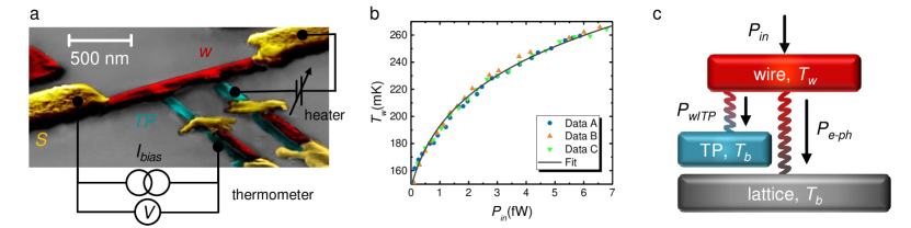
In order to obtain the electron-phonon coupling constant of the Al/Cu bilayer (), we injected a power directly into the wire and measured its electronic temperature (). To this end, we used a voltage-biased --- tunnel junction as heater and a current-biased --- JJ as thermometer giazotto , as shown in Fig. 6-a. Since we were interested in the normal-state coupling constant, we performed the experiments at mK (). The resulting versus characteristics are shown in Fig. 6-b. As expected, the electronic temperature of the wire monotonically increases by rising the injected power.
In order to analyze the experimental data, we have considered the thermal model shown in Fig. 6-c: the inward contribution of the heater () is balanced by the outward power flowing through the thermometer () and the electron-phonon relaxation channel (). The outward contributions through the Al banks can be neglected thanks to the Andreev mirror effect andreevl ; andreevll , since K. As a consequence, the energy balance equation of our system reads
| (11) |
In a temperature biased JJ, the power flowing from the normal electrode () to the superconducting tunnel electrode () is giazotto
| (12) |
where is the smeared normalized Bardeen-Cooper-Schrieffer (BCS) density of state of the superconducting Al electrode and is the Fermi-Dirac distribution of the , electrode, respectively. is the Dynes parameter accounting for the quasiparticle finite lifetime ( is an empirical parameter, is the superconducting energy gap at zero temperature: in our case and 182 eV), is the temperature dependent BCS energy gap, is the tunnel junction normal-state resistance, is the electron charge, is the Boltzmann constant and are the electronic temperatures of the , electrode, respectively ( due to the big volume of the tunnel probe leads).
The power loss due to the electron-phonon coupling of a normal metal element is giazotto
| (13) |
where is the volume of the wire, and are its electronic and phonon temperature wellstood , respectively.
By solving the Eq. 13 for , we computed the expected temperature of the wire active region as a function of . Since all the other device parameters are known, we fit our experimental data with Eq. 11 and extracted the values of . The resulting fitting curve is represented by the gray line in Fig. 6-b obtained for W/m3K5. Finally, we notice that, the extracted value of is in good agreement with the average of the coupling constants of Cu ( W/m3K5) and Al ( W/m3K5) giazotto , weighted on the ratio between the volumes of the two layers ( W/m3K5).
IX Reproducibility of the Josephson escape sensor
We investigated the behavior of a second JES. The device is nominally identical to the one presented in the main text. The samples were fabricated simultaneously (same electron beam lithography and angle resolved evaporation steps). Therefore, the differences in the critical current ( nA while nA) can be ascribed to small dissimilarities in the nanowires width.
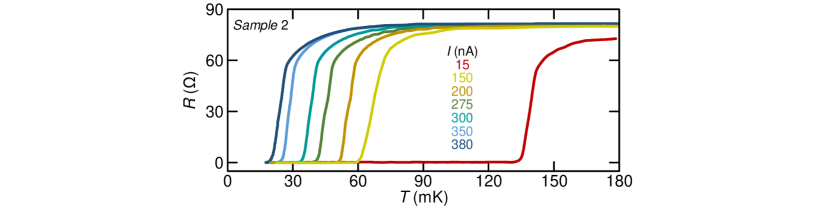
The resistance () versus temperature () characteristics of the second JES are shown in Fig. 7 for different values of bias current (). The device shows a normal state resistance , similar to that of the sample presented in the main text ( ). In agreement with the JES showed in the main text (see Fig. 3-a), by rising the transition from the superconducting to the dissipative state shifts towards lower temperature. In particular, the transition temperature shows a variation from about 140 mK at nA to about 23 mK at nA. Furthermore, the superconducting-to-dissipative state transition preserves the same appearance for every value of bias current.
The quantitative analysis of the dependence of the effective escape temperature () and transition width () on the bias current () is reported in the main text. In particular, the and dependence on the normalized current () of the two JESs are in good agreement, as shown in Fig. 3 of the main text.
X Performance of the JES and TES operation
The thermal model of the JES is depicted in Fig. 8. The input power () increases the electronic temperature of the one-dimensional JJ (). The two superconducting Al leads (kept at the bath temperature ) serve as Andreev mirrors andreevl ; andreevll , since K. Therefore, the electronic heat out-diffusion () is exponentially damped by the superconducting energy gap of Al and can be neglected. As a result, the only thermalization channel for the quasiparticles is the electron-phonon coupling ().
The JES is operated at that can be much smaller than the intrinsic wire critical temperature (): the sensor operates strongly in the superconducting state for high values of . Therefore, the electron-phonon coupling is exponentially damped by the presence of the superconducting gap Timofeev2009 ; Heikkila . On the contrary, in TES operation the nanowire is almost in the normal-state (, so that ), therefore the electron-phonon thermalization can be described by means of the normal metal thin film relation giazotto .
In the following we will show all the relations used to extract from our experimental data the principal figures of merit for the JES and the device operated as a conventional TES at about . In particular, we will calculate the thermal fluctuations limited noise equivalent power (), the frequency resolution () and the thermal time constants ( and ).

X.1 Figures of merit for the TES-mode operation
For a bolometer the NEP is limited by the thermal fluctuation noise giazotto . In case of TES operation (), the noise equivalent power can be written Bergmann
| (14) |
where describes the effect of the temperature gradient across the thermal link (with for a pure metal), is the thermal conductance of heat losses, and is the Boltzmann constant.
In our device the only channel for thermal losses is the electron phonon coupling (). Since at the JJ is partially dissipative, the electron-phonon coupling of a normal-metal diffusive thin film () described by Eq. 13 can be considered giazotto .
The thermal conductance for a TES () is obtained by calculating the derivative of with respect to the electronic temperature ()Irwin
| (15) |
where W m-3K-5 is the value derived from experimental measures, m-3 is the total volume of the Al/Cu bilayer, with and the aluminum and copper volumes, respectively.
In order to determine the performances of a sensor in single-photon detection, the frequency resolution () is the most used figure of merit. For a TES it reads Irwin
| (16) |
where is the Planck constant, is the electrothermal parameter accounting for sharpness of the phase transition from the superconducting to the normal-state Irwin , is the electron-phonon coupling for a pure metal and is the electron heat capacitance. It is interesting to note the strongly dependence on value which determines the negative electrothermal feedback (NETF) mechanism Irwin .
The electron heat capacitance is written
| (17) |
where is the Sommerfeld coefficient ( JK-2m-3 , JK-2m-3 for copper and aluminum, respectively). Moreover, for a TES the temperature variation after energy absorption is calculated by solving the time dependent energy balance equation that takes in account all the exchange mechanisms giazotto . In particular, the re-thermalization of the quasiparticles to shows an exponential dependence on time with constant
| (18) |
This is the intrinsic recovery time of the film which does not consider the Joule heating due to the current flowing through the sensor. Instead, including the heating term in the negative NETF configuration, the pulse recovery time becomes Irwin
| (19) |
which depends on (i.e. the main parameter of the NETF). When the pulse recovery time is much shorter than the intrinsic time constant (), the energy into the sensor is removed by decreasing its overheating, i.e., compensating for the initial temperature variation (NETF), instead of being dissipated through the substrate.
X.2 Figures of merit for the JES
The JES operates at the escape temperature , defined as the maximum temperature measured in the superconducting state before the transition to the dissipative state. Since the current injection does not change the energy gap of the wire (), the detector works deeply in the superconducting state since for high values of . Therefore, all figures of merit have to be calculated deeply in the superconducting state.
The thermal fluctuations limited noise equivalent power can be written
| (20) |
The thermal conductance in the superconducting state is described by Heikkila
| (21) |
where the first and the second terms refer to electron-phonon scattering and recombination processes, respectively. Here, is the Riemann zeta function, (with eV the experimental gap of the wire), is exchange field (0 in this case), with and with .
Operating as a calorimeter, the frequency resolution of a superconducting thermal sensor can be computed from Virtanen
| (22) |
where is the electron heat capacitance calculated at the escape temperature considering the damping term typical in a BCS superconductor
| (23) |
The low temperature exponential suppression with respect to the normal state heat capacitance, which leads to the JES high detection sensitivity, is written as Rabani
| (24) |
The electronic heat capacitance is given by
| (25) |
where the critical temperature mK is related to the measured gap eV.
Considering the relaxation time in the weak link, the predominant thermalization mechanism is due to the electron-phonon interaction, which defines the sensor relaxation half-time Virtanen
| (26) |
where is the thermal time constant (see Eq. 18) considering and for a Josephson escape sensor.
References
- (1) Tinkham, M. Introduction to Superconductivity (McGraw-Hill, 1996).
- (2) Ivanchenko, Yu. M., & Zil’berman, L. A. The Josephson effect in small tunnel contacts. Sov. Phys. JETP 28, 1272 (1969).
- (3) Bezryadin, A. Superconductivity in Nanowires: Fabrication and Quantum Transport (Wiley-VCH, 2012).
- (4) Ambegaokar, V., & Halperin, B. I. Voltage due to thermal noise in the dc Josephson effect. Phys. Rev. Lett. 22, 1364-1366 (1969).
- (5) Giazotto, F., Heikkilä, T. T., Luukanen, A., Savin, A. M. & Pekola, J.P. Opportunities for mesoscopics in thermometry and refrigeration: physics and applications. Rev. Mod. Phys. 78, 217–274 (2006).
- (6) Andreev A.F. Sov. Phys. JETP 19, 1228 (1964).
- (7) Andreev A.F. Sov. Phys. JETP 20, 1490 (1965).
- (8) Wellstood, F.C., Urbina, C. & Clarke, J. Hot-electron effects in metals. Phys. Rew. B 49, 5942 (1994).
- (9) Bergmann, T. Energy resolving power of transition edge x-ray microcalorimeters. Phd Dissertation University of Utrecht, (2004).
- (10) Timofeev, A. V., Pascual Giarcía, C., Kopnin, N. B., Savin, A. M., Meschke, M., Giazotoo, F., & Pekola, J. P. Recombination-Limited Energy Relaxation in a Bardeen-Cooper-Schrieffer Superconductor. Phys. Rev. Lett. 102, 017003 (2009).
- (11) Heikkil, T. T., Silaev M., Virtanen, P. & Bergeret, F. S. Thermal, electric and spin transport in superconductor/ferromagnetic-insulator structures. Progress in Surface Science 94, 100540 (2019).
- (12) Irwin, K. D. An application of electrothermal feedback for high resolution cryogenic particle detection. Applied Physics Letters 66, 1998-2000 (1995).
- (13) Virtanen, P., Ronzani, A. & Giazotto, F. Josephson photodetectors via temperature-to-phase conversion. Physical Review Applied 9, 054027 (2018).
- (14) Rabani, H., Taddei, F., Bourgeois, O., Fazio, R. & Giazotto, F. Phase-dependent electronic specific heat in mesoscopic josephson junction. Physical Review B 78, 012503 (2008).