Emergence of an upper bound to the electric field controlled Rashba spin splitting in InAs nanowires
Abstract
The experimental assessment of the strength () of the Rashba spin-orbit coupling is rather indirect and involves the measurement of the spin relaxation length from magnetotransport, together with a model of weak antilocalization. The analysis of the spin relaxation length in nanowires, however, clouds the experimental assessment of the and leads to the prevailing belief that it can be tuned freely with electric field–a central tenant of spintronics. Here, we report direct theory of leading to atomistic calculations of the spin band structure of InAs nanowires upon application of electric field– a direct method that does not require a theory of spin relaxation. Surprisingly, we find an upper bound to the electric field tunable Rashba spin splitting and the ensuing ; for InAs nanowires, is pinned at about 170 meVÅ irrespective of the applied field strength. We find that this pinning is due to the quantum confined stark effect, that reduces continuously the nanowire band gap with applied electric field, leading eventually to band gap closure and a considerable increase in the density of free carriers. This results in turn in a strong screening that prevents the applied electric field inside the nanowire from increasing further beyond around 200 kV/cm for InAs nanowires. Therefore, further increase in the gate voltage will not increase . This finding clarifies the physical trends to be expected in nanowire Rashba SOC and the roles played by the nano size and electric field.
pacs:
71.70.Ej, 73.21.Fg, 71.15.-mSpintronics offers the use of electron spin rather than electron charge to carry information, whereby the needed magnetic field is effectively provided by Rashba spin-orbit coupling (SOC) Dresselhaus (1955); Bychkov and Rashba (1984); Zhang et al. (2014) rather than by external magnetic field Nowack et al. (2007); Manchon et al. (2015). This opens a route towards electrical manipulation of electron spins Awschalom and Samarth (2009), such as that proposed in the Datta-Das spin transistor Datta and Das (1990) and spin qubits Nadj-Perge et al. (2010); Nowack et al. (2007). Such electrical manipulation instead of magnetic manipulation is particularly appealing for this purpose, because electric fields are easy to create locally on-chip, simply by exciting a local gate electrode Nowack et al. (2007).
One-dimensional semiconductor nanowires with strong SOC have recently emerged as promising building block for spintronics Nadj-Perge et al. (2010) and as a unique solid state platform for realizing and observing the Majorana fermions Oreg et al. (2010); Lutchyn et al. (2010); Mourik et al. (2012); Das et al. (2012). However, despite such interest of SOC in 1D wires, they have been studied far less than in 3D bulk semiconductors Dresselhaus (1955); Luo et al. (2009a); Ishizaka et al. (2011); Zhang et al. (2014) and in 2D heterostructures Bychkov and Rashba (1984); Winkler (2003) and quantum wells Winkler (2003); Luo et al. (2010). Here we focus on the assessment of the strength of the Rashba SOC () and its dependence on the applied external electric field. The prevailing practice to deduce Rashba parameter is to measure the spin relaxation length from magnetotransport measurements requiring an analysis of weak antilocalization Dhara et al. (2009); Estévez Hernández et al. (2010); Liang and Gao (2012); van Weperen et al. (2015). Considering that the D’yakonov-Perel’ (DP) mechanism a primary spin-relaxation in 3D bulk and 2D quantum wells is considerably suppressed in 1D nanowires Kiselev and Kim (2000); Pareek and Bruno (2002); Pramanik et al. (2005); Kaneko et al. (2008); Holleitner et al. (2006); Kettemann (2007) and the inter-subband scattering induced spin-relaxation becomes dominate, the experimentally deduced Rashba parameter in 1D nanowires from magnetotransport measurements may be uncertain because unlike the former the latter is independent on .
In this work, we provide a theoretical evaluation of in InAs nanowires using a direct method that does not require a theory of spin relaxation. We do so by solving the Schrödinger equation for a nanowire experiencing a perpendicular electric field, obtaining the spin-dependent band structure (see Fig. 1(b) for a 30 nm InAs nanowire), from which we directly obtain the spin splitting by subtracting the band energies of the branches with two spin directions. We then fit the obtained spin splitting of the lowest conduction subband to a wavevector power series: and thus find directly the Rashba parameter . We study electron for InAs nanowires as a function of nanowire size and electric field. Our central finding is that there is an upper bound to the strength of the field-induced Rashba SOC owing to the quantum-confined stark effect (QCSE). This finding explains the size-independence and field-independence of = 200 meVÅ of InAs nanowires observed in a recent experiment Roulleau et al. (2010). This finding clarifies the physical trends to be expected in nanowire Rashba SOC, sets realistic expectations to nanowire spintronics applications, and resolves the experimental puzzle of occasional failure to raise persistently with gate voltage in nanowires Hansen et al. (2005); Dhara et al. (2009); Estévez Hernández et al. (2010); Roulleau et al. (2010); Liang and Gao (2012).
Atomistic calculation of the Rashba Spin splitting in nanowires under applied electric field.
In the approaches for studying the Dresselhaus and Rashba SOC in low-dimensional structures Kloeffel et al. (2011); Zhang and Xia (2006, 2007); Winkler (2003), one uses a phenomenological Hamiltonian where one needs to decide at the outset which 3D bulk bands couple in low-dimensional structures by the SOC and crystal field. The potential of missing important physical interactions, such as heavy-hole and light-hole band coupling, not selected to be present in certain model Hamiltonian can be substantial to describe SOC induced spin splitting Luo et al. (2011, 2010); Luo and Zunger (2010). Here we adopt instead an atomistic pseudopotential method in which the low-dimensional structure is viewed as a giant molecular system in its own right, rather than express it in terms of a pre-selected basis drawn from a reference 3D bulk system. This method has been tested extensively over the past two decades for a broad range of spectroscopic quantities in self-assembled and colloidal nanostructures Bester and Zunger (2005); Luo et al. (2009b, 2015), as well as been previously applied to investigate Dresselhaus SOC in 3D zinc-blends semiconductors Luo et al. (2009a), 2D quantum wells Luo et al. (2010); Luo and Zunger (2010), and 1D nanowires Luo et al. (2011).
The band structure of 1D nanowire is obtained via direct-diagonalization of the Schrödinger equation Luo et al. (2011, 2009a); Bester and Zunger (2005),
| (1) |
The crystal potential is a superposition of screened atomic potentials of atom type located at atomic site . The screened atomic potential contains a local part and a nonlocal spin-orbit interaction part which is treated as local in the Kleinman-Bylander scheme Kleinman and Bylander (1982). is applied electric field Bester and Zunger (2005); Yu and Cardona (2005); Winkler (2003), which is generally created in devices by exciting a local gate electrode Nowack et al. (2007). Here, applied in the -direction, perpendicular to the nanowire axis -direction. The construction of the screened pseudopotenttial is the key to accuracy and realism. To remove the “LDA error” in the bulk crystal we fit the atomic potentials to experimental transition energies, effective masses, spin-orbit splitting, and deformation potentials of the parent bulk semiconductors as described previously Williamson et al. (2000). The InAs nanowires are embedded in an artificial material with the same lattice as InAs but much wider bandgap and heavier masses Wang et al. (2015). For more details on screened pseudopotentials of InAs and barrier material used here see Refs. Williamson et al. (2000); Wang et al. (2015).
Closed form physical model for Rashba electron term in nanowires.
A comparison of between atomistic pseudopotential calculations and the classical model Hamiltonian approach may provide insight into the understanding of the Rashba spin splitting. The term of the Rashba SOC, which originates from the spin-orbit interaction, in an effective conduction band Hamiltonian is arising from the non-commutativity of wavevector and crystal potential from a decoupling of conduction and valence band states Winkler (2003). If one uses the Kane Hamilotonian, third-order perturbation theory for the conduction band Hamiltonian yields the Rashba SOC term Winkler (2003),
| (2) |
where is the electric field contained implicitly in the crystal potential , here, is arising from applied electric field . the vector of Pauli spin matrices, and a material-specific Rashba coefficient Winkler (2003),
| (3) |
Where is electron charge, the band gap of quantum structures, the spin-orbit splitting ( eV for bulk InAs), and Kane’s momentum matrix element ( eV for bulk InAs). The adjustable parameter is used to take into account all factors missed in classical Hamiltonian approach, such as (i) inter-band coupling induced by space confinement rather than by ; (ii) Change of the quantum confinement potential induced modification of dipole matrix element ; (iii) Energy level splitting of the valence bands; and (iv) QCSE as discussed below. The Rashba SOC induced spin splitting of the conduction subband is , here the pre-factor is the named Rashba parameter,
| (4) |
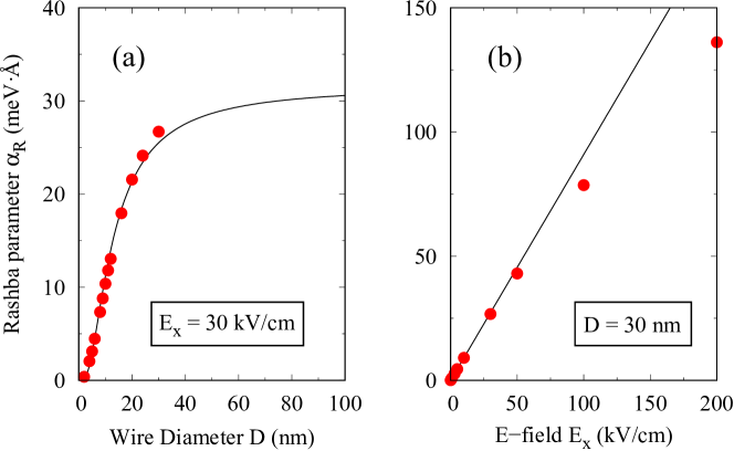
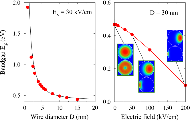
The value of could be inferred by fitting atomistic predicted to Eq. (4). In doing so, we first describe atomistic predicted of InAs nanowires with diameter by a formula as shown in Fig. 3 (a), here eV is bulk InAs band gap Vurgaftman et al. (2001), and and for InAs nanowires under kV/cm. Taking as the only adjustable parameter, we subsequently fit atomistic predicted to Eq. (4), shown in Fig. 2 (a). Our best fit indicates . This value is close to for the rectangular well and for the parabolic well Winkler (2003), with an infinite energy barrier Winkler (2003), implying that the contributions from missed four factors to are small, at least for nanowires under a moderate electric field of kV/cm.
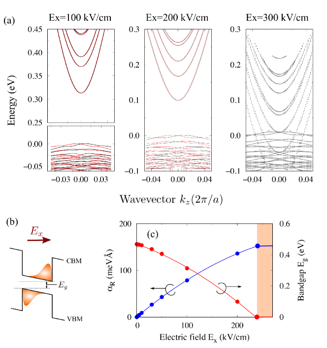
Dependence of on wire diameter and applied field: the emergence of saturation.
Our recent work Luo et al. (2011) on spin splitting in zinc-blende nanowires established based on fundamental nanowire symmetry that the Dresselhaus spin splitting is absent in the (001)- and (111)-oriented nanowires with such tetrahedral bonding. An electric field applied perpendicular to the wire direction breaks the symmetry but does not evoke the Dresselhaus spin splitting, even if such spin splitting is present in 3D bulk InAs and 2D quantum wells. The field-induced spin splitting is exclusively due to the Rashba SOC effect Luo et al. (2011). In the following we apply the electric field perpendicular to the (001)-oriented InAs zinc-blende nanowires; the obtained spin splitting (Fig. 1 (a)) is thus exclusively due to the Rashba effect. In early reports Glas et al. (2007); Johansson et al. (2010), small ( nm) diameter III-V nanowires showed a tendency toward forming a wurtzite phase. In recent reports, however, both pure ZB and pure WZ nanowires could be achieved across the broad range of nanowire diameters Joyce et al. (2010); Zhao et al. (2014); Fu et al. (2016). Zinc-blende InAs nanowires as small as 15 nm in diameter were routinely synthesized Fu et al. (2016).
Fig. 2 shows atomistic calculated in InAs nanowires as a function of wire diameter for a fixed electric field. Upon application of a fixed electric field kV/cm, Fig. 2 (a) exhibits that increases rapidly to 21.5 meVÅ up to nm and begins to saturate to 34 meVÅ (a value of bulk InAs) as further increasing the nanowire diameter for InAs nanowires. The best fit of atomistic predicted to Eq. (4), as shown in Fig. 2 (a) by a back curve, indicates a good agreement between atomistic method and classical model Hamiltonian approach for Rashba SOC. Fig. 2 (b) shows the field-dependence of for a nm InAs nanowire which is linear until kV/cm and then becomes sublinear as further increasing . It clearly manifests that the Rashba SOC is strongly field tunable: increases from zero at the absence of electric field to as large as 136 meVÅ at kV/cm. The slope in the linear region determines the Rashba coefficient eÅ2, which is consistent with bulk InAs of eÅ2 Winkler (2003) with a small difference owing to quantum confinement effect, indicating the robustness of the used atomistic pseudopotential method to predict the Rashba effect.
Effect of electric field on through electron-hole charge separation: the QCSE.
When an external electric field is applied perpendicularly to a nanowire, the electron states shift to lower energies, while the hole states shift to higher energies, reducing the nanowire band gap , as shown in Fig. 3 (b). Additionally, the external electric field shifts electrons and holes to opposite sides along the electric field within the nanowire cross-section, see insets to Fig. 3 (b) and Fig. 1 (b), decreasing the overlap integral, which in turn reduces the recombination efficiency (i.e., fluorescence quantum yield) of the system. This effect is the so-called QCSE. The QCSE modifies explicitly via shifting the energy levels, at the same time, changes implicitly by reducing the overlap of the wave functions of the conduction and valence subbands and subsequently decreasing the matrix elements. We expect stronger QCSE under the larger electric field. To examine the modification of induced by QCSE in nanowires, we investigate the evolution of the as a function of electric field for a nm nanowire, as shown in Fig. 2 (b). It exhibits the field-dependence of the being sublinear instead of expected linear from the classical model Hamiltonian approach (will be discussed below). Specifically, the field-dependence of the is almost linear until kV/cm and then becomes sublinear as further increasing . The sublinear behavior is a result of QCSE, and a larger deviation from the linear function of illustrates a stronger QCSE on . This result is consistent with what we have discussed above that the QCSE on is negligible under kV/cm.
Emergence of an upper bound for Rashba parameter in nanowires.
Figure 3 (b) shows the QCSE induced shifting of the band gap for a nm InAs nanowire. We see that the QCSE shifts the nanowire to a smaller value continuously and finally to as low as 0.05 eV at kV/cm. Further increase of will ultimately close the bandgap and make the nanowire metallic, which leads to considerable increase in free carrier density in the nanowires and produces a giant screening which in turn prevents the electric field inside the nanowire from further increasing. In experimental devices, the magnitude of the electric field applied across the nanowires are tuned indirectly by a gate voltage. Although one may increase the gate voltage as large as to tens Volts Liang and Gao (2012), the electric field falling inside the nanowire is pinned to a value once it closes the nanowire bandgap owing to the QCSE. To further increase gate voltage above pinned electric field, the additional voltage will drop across the matrix outside the nanowires. Therefore, the QCSE gives rise to an upper limit of the reachable electric field, which is around 200 kV/cm for InAs nanowires. The predicted meVÅ at kV/cm is thus a maximum achievable value for the nm InAs nanowire, as shown in Fig. 1 (c). Considering that increases slightly in thicker nanowires, we estimate an upper bound for being about 170 meVÅ for InAs nanowires.
Comparison between theoretical predictions and experimental measurements of Rashba parameter .
The maximum available electric field and the strength of the Rashba SOC in nanowires have frequently observed in the experimental measurements Hansen et al. (2005); Dhara et al. (2009); Estévez Hernández et al. (2010); Roulleau et al. (2010); Liang and Gao (2012), but has not recognized as essential physical effects. Regarding the classical model Hamiltonian, Rashba parameter is expected to be simply proportional to the magnitude of applied electric field. We thus believe that we could always increase the strength of the Rashba SOC via increasing the gate voltage applied to the nanowires Liang and Gao (2012). However, experiments often failed to realize it Hansen et al. (2005); Dhara et al. (2009); Estévez Hernández et al. (2010); Roulleau et al. (2010); Liang and Gao (2012). We demonstrate from atomistic calculations that there exists an upper bound to for each nanowires, thus clarifying the experimental puzzle of failure to raise persistently with gate voltage in nanowires Hansen et al. (2005); Dhara et al. (2009); Estévez Hernández et al. (2010); Roulleau et al. (2010); Liang and Gao (2012).
The general practice to deduce the strength of Rashba parameter is to measure the spin relaxation length from magnetotransport measurements requiring an analysis of weak antilocalization Dhara et al. (2009); Estévez Hernández et al. (2010); Liang and Gao (2012); van Weperen et al. (2015). In the dirty metal regime (where the electron elastic-scattering length is smaller than the wire diameter ) Roulleau et al. (2010), the ballistic spin-precession length , and subsequently . Experimentally reported for InAs nanowires has covered a wide range of meVÅ Hansen et al. (2005); Dhara et al. (2009); Estévez Hernández et al. (2010); Roulleau et al. (2010); Liang and Gao (2012). Note that the wire geometries and expressions for used by different groups vary and that often only Liang and Gao (2012); Hansen et al. (2005); Dhara et al. (2009); Estévez Hernández et al. (2010), not Roulleau et al. (2010); van Weperen et al. (2015), is evaluated. Using to calculate via , Roulleau et al. Roulleau et al. (2010) got a same Rashba coupling parameter of = 200 meVÅ, under large gate voltage, for all three investigated InAs nanowires with diameters of 75, 140, and 217 nm, respectively. Such observed size-independence and field-independence of = 200 meVÅ supports well our prediction of the emergence of an upper bound of meVÅ for InAs nanowires upon application of electric field.
We also note that a considerable suppression of the DP spin-relaxation, which usually dominates the spin-relaxation in semiconductors, in 1D nanowires has been predicted theoretically Kiselev and Kim (2000); Pareek and Bruno (2002); Pramanik et al. (2005); Kaneko et al. (2008) and observed experimentally Holleitner et al. (2006); Kettemann (2007). The DP mechanism is owing to the randomizing of the momentum-dependent Rashba SOC-induced effective magnetic field. In single-channel (i.e., single-band) clean 1D nanowires, where the electron elastic-scattering length is larger than the wire diameter , the spin-relaxation is even completely suppressed due to a dimensionally constrained DP mechanism Kiselev and Kim (2000); Pramanik et al. (2005); Kaneko et al. (2008). Whereas, in multiple-channel 1D nanowires, the inter-subband scattering enables the spin-relaxation Pramanik et al. (2005); Kaneko et al. (2008). Considering the inter-subband scattering induced spin-relaxation dependents mainly on the occupation of excited subbands, rather than on the strength of Rashba SOC, the experimentally deduced Rashba parameter in 1D nanowires from magnetotransport measurements may uncertain.
Interestingly, the conclusions regarding the Rashba parameter drawn from zinc-blende nanowires are also applicable to the wurtzite phase (as well as to different nanowire orientations and shapes). The reason for this is that the strength of the Rashba SOC for a given material dependents primarily on the nanowire band gap and is rather insensitive to geometric and crystal parameters that result in a particular band gap value. The excellent agreement between the atomistic method and classical model Hamiltonian on the prediction of , as shown in Fig. 2 (a), evidences it, since the model deduced in Eq. (S3) applies to both 2D and 1D electrons Winkler (2003); Zhang and Xia (2006) without considering the crystal orientations and wire shapes. Eq. (1) is well justified only for dielectric phase. Under the conditions when electron and hole densities develop at opposite edges of the wire, they produce additional electric potential, and, hence, a self-consistent Poisson-Schrodinger problem should in principle be solved. In other words, Eq. (1) is valid only until the dielectric stays constant, and narrowing of the gap seems to violate this condition. We did not perform such corrections. Indeed, we study charge neutral nanowires by specifying the Fermi level located in the middle of the band gap, and the applied electric field being uniform across the nanowire. A self-consistent simulation would depend on a range of device parameters such as the distance from the gate to the nanowire; the nature of the gate contact to the nanowire, the nature of the insulating layers between them, the doping levels and the dopant concentration inside the nanowire. Such quantities often vary from sample to sample and are not always cited in the experimental papers. Note, however, that the Rashba SOC is not dependent on the detailed profile of the local electric field because it is proportional to the expectation value of the external field as pointed out in Ref. Winkler (2003). Hence, we can approximate the Rashba SOC by solving only the Schrodinger equation with an assumption of a constant (non-self-consistent) electric field across the nanowire cross-section. This approximation has been shown previously to be successful in reproducing the experimentally measured Rashba parameters as reported in literature Winkler (2003).
Electron Rashba spin-orbit energy for Majorana detection experiments:
Semiconductor nanowires were recently recognized to be a unique solid state platform for realizing and observing the Majorana fermions – unique particles that are identical to their own antiparticles, and forming bound states with non-Abelian exchange statistics and suitable as the building blocks of quantum computer Stern and Lindner (2013). Specifically, the Majorana fermions were recently detected within the topological band gap of hybrid superconductor-semiconductor InAs Das et al. (2012) or InSb nanowires Mourik et al. (2012), respectively, following the theoretical proposal Oreg et al. (2010); Lutchyn et al. (2010). This experiment requires large SOC-induced Rashba spin splitting since it determines the size of the topological gap that needs to exceed at the temperature at which experiment is performed. Therefore, InAs or InSb nanowires were employed in Majorana fermion experiments considering bulk InAs and InSb have strong spin-orbit interactions Mourik et al. (2012); Das et al. (2012).
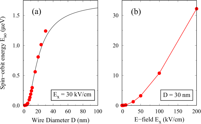
In Majorana fermion experiments, Rashba spin-orbit energy of the investigated nanowires is a critical parameter because it limits the size of the applied magnetic field opened topological gap that needs to exceed the temperature at which the experiments of Majorana fermions are carried out Mourik et al. (2012); Das et al. (2012). is also estimated indirectly from experimental measurement. Here, we could directly obtain and its dependence on field and diameter from the calculations of which is shown in Fig. 2 in the main text. Fig. 4 shows of the lowest electron subband for InAs nanowires. We see that, under a moderate electric field of 30 kV/cm, is unexpected small (less than 2 eV) and is far less than the minimum value required for hosting Majorana fermions. A large electric field is thus expected to considerably increase so as to meet the requirements of Majorana fermion experiments, such as Ref. Das et al. (2012) and Ref. Mourik et al. (2012) cite and 50 eV for InAs and InSb nanowires, respectively. Instead, Fig. 4(c) shows that an extremely large electric field of kV/cm is needed to tune to the maximal achievable value of 32 eV for a nm InAs nanowire.
In summary, we have studied the Rashba SOC directly in InAs nanowires by performing SOC band structure calculations using all-band atomistic pseudopotential approach, without unambiguous as occured in experimental measurements. We uncovered the existence of an upper bound of the strength of the electric field tunable Rashba SOC in semiconductor nanowires as increasing the gate voltage. We found that it is a result of the QCSE, which lowers the nanowire band gap as the applied electric field increases continuously, and finally, closes the band gap rendering the nanowire metallic. The metallic nanowires have a giant screening to prevent the electric field from further rising in the nanowire, and thus further increase the gate voltage will not increase the electric field, and thus . The revealed upper bound of meVÅ explains the size-independence and field-independence of = 200 meVÅ of InAs nanowires observed in a recent experiment Roulleau et al. (2010). We believe that we have clarified the experimental puzzle of failure to raise persistently with gate voltage in nanowires Hansen et al. (2005); Dhara et al. (2009); Estévez Hernández et al. (2010); Roulleau et al. (2010); Liang and Gao (2012), making a fundamental step towards the understanding of the Rashba SOC in semiconductor nanowires.
Acknowledgements.
The work in China was supported by the National Science Foundation of China (NSFC grants #61888102 and #11925407). AZ was supported by Office of Science, Basic Energy Science, MSE division under grant DE-FG02-13ER46959 to CU Boulder.References
- Dresselhaus (1955) G. Dresselhaus, Physical Review 100, 580 (1955).
- Bychkov and Rashba (1984) Y. A. Bychkov and E. I. Rashba, Journal of Physics C: Solid State Physics 17, 6039 (1984).
- Zhang et al. (2014) X. Zhang, Q. Liu, J.-w. Luo, A. J. Freeman, and A. Zunger, Nature Physics 10, 387 (2014).
- Nowack et al. (2007) K. C. Nowack, F. H. L. Koppens, Y. V. Nazarov, and L. M. K. Vandersypen, Science (New York, N.Y.) 318, 1430 (2007).
- Manchon et al. (2015) A. Manchon, H. C. Koo, J. Nitta, S. M. Frolov, and R. A. Duine, Nature Materials 14, 871 (2015).
- Awschalom and Samarth (2009) D. Awschalom and N. Samarth, Physics 2, 50 (2009).
- Datta and Das (1990) S. Datta and B. Das, Applied Physics Letters 56, 665 (1990).
- Nadj-Perge et al. (2010) S. Nadj-Perge, S. M. Frolov, E. P. A. M. Bakkers, and L. P. Kouwenhoven, Nature 468, 1084 (2010).
- Oreg et al. (2010) Y. Oreg, G. Refael, and F. von Oppen, Physical Review Letters 105, 177002 (2010).
- Lutchyn et al. (2010) R. M. Lutchyn, J. D. Sau, and S. Das Sarma, Physical Review Letters 105, 077001 (2010).
- Mourik et al. (2012) V. Mourik, K. Zuo, S. M. Frolov, S. R. Plissard, E. P. A. M. Bakkers, and L. P. Kouwenhoven, Science 336, 1003 (2012).
- Das et al. (2012) A. Das, Y. Ronen, Y. Most, Y. Oreg, M. Heiblum, and H. Shtrikman, Nature Physics 8, 887 (2012).
- Luo et al. (2009a) J.-W. Luo, G. Bester, and A. Zunger, Physical Review Letters 102, 056405 (2009a).
- Ishizaka et al. (2011) K. Ishizaka, M. S. Bahramy, H. Murakawa, M. Sakano, T. Shimojima, T. Sonobe, K. Koizumi, S. Shin, H. Miyahara, A. Kimura, K. Miyamoto, T. Okuda, H. Namatame, M. Taniguchi, R. Arita, N. Nagaosa, K. Kobayashi, Y. Murakami, R. Kumai, Y. Kaneko, Y. Onose, and Y. Tokura, Nature Materials 10, 521 (2011).
- Winkler (2003) R. Winkler, Spin-orbit coupling effects in two-dimensional electron and hole systems, Springer tracts in modern physics No. v. 191 (Springer, Berlin ; New York, 2003).
- Luo et al. (2010) J.-W. Luo, A. N. Chantis, M. van Schilfgaarde, G. Bester, and A. Zunger, Physical Review Letters 104, 066405 (2010).
- Dhara et al. (2009) S. Dhara, H. S. Solanki, V. Singh, A. Narayanan, P. Chaudhari, M. Gokhale, A. Bhattacharya, and M. M. Deshmukh, Physical Review B 79, 121311 (2009).
- Estévez Hernández et al. (2010) S. Estévez Hernández, M. Akabori, K. Sladek, C. Volk, S. Alagha, H. Hardtdegen, M. G. Pala, N. Demarina, D. Grützmacher, and T. Schäpers, Physical Review B 82, 235303 (2010).
- Liang and Gao (2012) D. Liang and X. P. Gao, Nano Letters 12, 3263 (2012).
- van Weperen et al. (2015) I. van Weperen, B. Tarasinski, D. Eeltink, V. S. Pribiag, S. R. Plissard, E. P. A. M. Bakkers, L. P. Kouwenhoven, and M. Wimmer, Physical Review B 91, 201413 (2015).
- Kiselev and Kim (2000) A. A. Kiselev and K. W. Kim, Physical Review B 61, 13115 (2000).
- Pareek and Bruno (2002) T. P. Pareek and P. Bruno, Physical Review B 65, 241305 (2002).
- Pramanik et al. (2005) S. Pramanik, S. Bandyopadhyay, and M. Cahay, IEEE Transactions On Nanotechnology 4, 2 (2005).
- Kaneko et al. (2008) T. Kaneko, M. Koshino, and T. Ando, Physical Review B 78, 245303 (2008).
- Holleitner et al. (2006) A. W. Holleitner, V. Sih, R. C. Myers, A. C. Gossard, and D. D. Awschalom, Physical Review Letters 97, 036805 (2006).
- Kettemann (2007) S. Kettemann, Physical Review Letters 98, 176808 (2007).
- Roulleau et al. (2010) P. Roulleau, T. Choi, S. Riedi, T. Heinzel, I. Shorubalko, T. Ihn, and K. Ensslin, Physical Review B 81, 155449 (2010).
- Hansen et al. (2005) A. E. Hansen, M. T. Björk, C. Fasth, C. Thelander, and L. Samuelson, Physical Review B 71, 205328 (2005).
- Kloeffel et al. (2011) C. Kloeffel, M. Trif, and D. Loss, Physical Review B 84, 195314 (2011).
- Zhang and Xia (2006) X. W. Zhang and J. B. Xia, Physical Review B 74, 075304 (2006).
- Zhang and Xia (2007) X. W. Zhang and J. B. Xia, Journal of Physics D: Applied Physics 40, 541 (2007).
- Luo et al. (2011) J.-W. Luo, L. Zhang, and A. Zunger, Physical Review B 84, 121303 (2011).
- Luo and Zunger (2010) J.-W. Luo and A. Zunger, Physical Review Letters 105, 176805 (2010).
- Bester and Zunger (2005) G. Bester and A. Zunger, Phys. Rev. B 72, 165334 (2005).
- Luo et al. (2009b) J.-W. Luo, G. Bester, and A. Zunger, New Journal of Physics 11, 123024 (2009b).
- Luo et al. (2015) J.-W. Luo, G. Bester, and A. Zunger, Physical Review B 92, 165301 (2015).
- Kleinman and Bylander (1982) L. Kleinman and D. M. Bylander, Physical Review Letters 48, 1425 (1982).
- Yu and Cardona (2005) P. Y. Yu and M. Cardona, Fundamentals of semiconductors: physics and materials properties, 3rd ed. (Springer, Berlin, 2005).
- Williamson et al. (2000) A. J. Williamson, L. W. Wang, and A. Zunger, Phys. Rev. B 62, 12963 (2000).
- Wang et al. (2015) J. Wang, J.-W. Luo, L. Zhang, and A. Zunger, Nano Letters 15, 88 (2015).
- Vurgaftman et al. (2001) I. Vurgaftman, J. R. Meyer, and L. R. Ram-Mohan, Journal of Applied Physics 89, 5815 (2001).
- Glas et al. (2007) F. Glas, J.-C. Harmand, and G. Patriarche, Physical Review Letters 99 (2007), 10.1103/PhysRevLett.99.146101.
- Johansson et al. (2010) J. Johansson, K. A. Dick, P. Caroff, M. E. Messing, J. Bolinsson, K. Deppert, and L. Samuelson, The Journal of Physical Chemistry C 114, 3837 (2010).
- Joyce et al. (2010) H. J. Joyce, J. Wong-Leung, Q. Gao, H. H. Tan, and C. Jagadish, Nano Letters 10, 908 (2010).
- Zhao et al. (2014) Y. Zhao, X. Li, W. Wang, B. Zhou, H. Duan, T. Shi, X. Zeng, L. Ning, and Y. Wang, Journal of Semiconductors 35, 093002 (2014).
- Fu et al. (2016) M. Fu, Z. Tang, X. Li, Z. Ning, D. Pan, J. Zhao, X. Wei, and Q. Chen, Nano Letters 16, 2478 (2016).
- Stern and Lindner (2013) A. Stern and N. H. Lindner, Science 339, 1179 (2013).