Large Enhancement of Critical Current in Superconducting Devices by Gate Voltage
Abstract
Significant control over the properties of a high-carrier density superconductor via an applied electric field has been considered infeasible due to screening of the field over atomic length scales. Here, we demonstrate an enhancement of up to 30 % in critical current in a back-gate tunable NbN, micro- and nano superconducting bridges. Our suggested plausible mechanism of this enhancement in critical current based on surface nucleation and pinning of Abrikosov vortices is consistent with expectations and observations for type-II superconductor films with thicknesses comparable to their coherence length. Furthermore, we demonstrate an applied electric field dependent infinite electroresistance and hysteretic resistance. Our work presents an electric field driven enhancement in the superconducting property in type-II superconductors which is a crucial step towards the understanding of field-effects on the fundamental properties of a superconductor and its exploitation for logic and memory applications in a superconductor-based low-dissipation digital computing paradigm.
NEST, Instituto Nanoscienze-CNR and Scuola Normale Superiore, I-56127 Pisa, Italy \altaffiliationContributed equally to this work \altaffiliationContributed equally to this work \alsoaffiliationFísica de Materiais, Universidade de Pernambuco, Recife, 50720-001, Brazil \alsoaffiliationDepartment of Physics, Massachusetts Institute of Technology, Cambridge, MA-02139, USA
Keywords: NbN, Superconducting nano-bridges, Gate-tunability, Critical current, Electroresistance, Vortices.
1 Introduction
Semiconductor-based field-effect transistors (FETs), which have been instrumental in the silicon revolution, operate through modulation of resistance between the source and drain electrodes via an applied gate voltage. This modulation, in turn, is achieved via a change in the charge carrier density resulting from the electric field generated by the gate voltage. The relatively low carrier densities in semiconductors allows for a strong resistance modulation with reasonable gate voltages thereby enabling broad functionalities. Such a field effect is not expected to work with metals, which have a very high charge density compared to what can be induced by a gate voltage, and was shown to be negligibly weak 1, 2.
Gate-voltage modulation of superconductivity is considered immensely useful, and has been attempted for some time 3, 4, 5, 6, including the recent advances in gate tunability of superconductivity in Van der Waals materials 7, 8, 9. Conventional superconductors have been amenable to control via interaction with magnetic fields 10, 11, 12, 13, 14, 15, but not electric fields. Superconducting properties, such as critical temperature of metallic superconductors, were found to be fairly insensitive to gate voltages 3, 16, exhibiting a minuscule change of . In contrast, unconventional superconductors based on strongly correlated oxides allow for an efficient gate-modulation due to their relatively low carrier concentration 5, 6, 4. The change in density of states at the chemical potential, which is associated with the gate-modulated carrier density, alters the superconducting order parameter and qualitatively explains the experimental observations discussed above 6, 16. This implies that superconducting properties, such as , can be enhanced (reduced) by an increase (decrease) in the carrier concentration via a positive (negative) gate voltage. The change in superconducting properties is thus odd in the gate voltage, i.e. unipolar. Besides this quasi-equilibrium modulation, various nonequilibrium approaches to controlling the superconducting properties using electromagnetic radiation have been successful, with significant advances demonstrated recently 17, 18.
In contrast with previous literature and expectations 19, 16, De Simoni and coworkers recently reported a gate-voltage-induced suppression of the critical current () in all-metallic superconducting nano-bridges and junctions 20, 21, 22, 23. Furthermore, the observed suppression is even in the gate voltage, i.e. bipolar. Apart from the technological potential, these observations have raised two fundamental questions regarding (i) how a gate-voltage-induced electric field can affect a high-carrier density superconductor 19, 24, 16, 3, 25, and (ii) what mechanism causes a change in the . These crucial issues remain unaddressed thus far, although the possibility of metallic puddles creation 26, that could reduce the , has been floated. Various other mechanisms that may degrade superconductivity could be envisaged as accounting for the observed reduction; for instance injection of high-energetic carriers as established by two most recent experiments with compelling evidences considering the size of leakage currents 27, 28.
Here, we demonstrate a bipolar gate-voltage-induced enhancement in the of NbN (high carrier density superconductor) based superconducting bridges by 30, while the critical temperature remains insensitive to the applied voltage. Besides uncovering novel fundamental phenomena, we demonstrate infinite electroresistance, i.e. gate-voltage-controlled change in resistance between zero and a finite value, and hysteretic resistance variation vs. gate voltage. These two effects could be exploited for low-dissipation logic and memory elements based on superconductors. We further demonstrate that the observed phenomena work for bridges in the nanoscale providing a proof-of-principle for scalability of such a technological paradigm. We also qualitatively discuss a plausible mechanism for the observed critical current modulation with the gate voltage. Hypothesizing that the critical current in our films is the value at which flux creep from one edge to the other becomes energetically favorable 29, 30 by overcoming Bean-Livingston surface barrier 31, a gate-voltage-induced enhancement of this surface barrier could account for our experiments and is consistent with related literature 29, 30, 32, 33, 34, 35. Altogether, our work provides crucial insights for understanding the field effect in metallic superconductors demonstrating that it could be further optimized with suitable surface termination and employed for enhancing, instead of suppressing, superconducting properties.
2 Synthesis and Fabrication
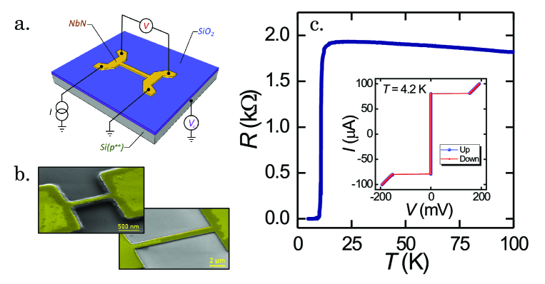
Niobium nitride (NbN) thin films with thicknesses nm and nm were grown on Si/SiO2 substrates (Fig. 1). The 300 nm thick SiO2 layer ensured electrical isolation between the superconducting film and the p-doped Si substrate acting as the gate. NbN thin films with Al2O3 ( nm) capping were grown in situ by reactive DC magnetron sputtering (for NbN) and by standard RF non-reactive magnetron sputtering (for Al2O3). Substrates were annealed at 573 K for 1 hour in UHV prior to the deposition. The base pressure of the sputtering chamber before the film deposition was below 5 10-8 Torr. The thin film growth was found to be poly-crystalline in texture with sharp, well defined NbN characteristic peaks in x-ray diffraction spectrum (see supplementary information). The multilayer structures were then patterned via e-beam lithography into a microbridge (B), with length m, width m, and thickness nm, and a nanobridge (NB) with m, nm, and nm (Fig. 1). Negative-tone resist was spun on the film and exposed at 10 kV following a soft bake. The resulting pattern was developed and the samples were then Ar+ ion-milled to fabricate the bridges.
3 Results
We first present our experiments on the B device. It was cooled down below its transition temperature into the superconducting state. A transition temperature Tc 10.8 K can be seen in the temperature dependence of resistance shown in Fig. 1(c), similar to previous NbN thin films, (for example – ref.36). The inset depicts the corresponding I-V characteristics at 4.2 K showing a of about 82.5 A. The Bardeen-Cooper-Schrieffer (BCS) energy gap 2 = 4.05 kBTc corresponds to 4.16 meV, where kB is Boltzmann constant 37, 38. The London penetration depth is derived from the above parameters as nm, where m, m, and nm are length, width, and thickness of the bridge, respectively. = 2 k is the resistance in the normal state at low temperature, and is magnetic permeability in vacuum. The Ginzburg-Landau coherence length is estimated as nm, where is the density of states in NbN at Fermi level 39 and is the electronic charge. This places the Pearl length 40, 41 () at around 40 m ( ) ensuring a spatially uniform current through the film.
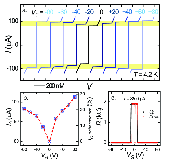
Further, the same B was investigated for its electric field response by applying back-gate voltage as depicted in Fig. 1(a). Figure 2 (a) shows current-voltage characteristics of the B at different back-gate voltages ( varying from -80 V to +80 V) at 4.2 K. The enhances with increase in gate voltage from 80 A to 105 A (i.e., an increase in critical current density, from 0.80 Acm-2 to 1.03 Acm-2). The enhancement shows a nearly symmetric response with respect to the gate voltage polarity [Fig. 2 (b)] and is observed to be 30% which is the largest modulation to date 20. The applied voltage, however, did not produce any observable change in the critical temperature. As discussed below, the observed enhancement in the , as compared to the previously reported suppression 20, may be attributed to our choice of superconductor (type II) and the film thickness, that is comparable to the superconducting coherence length.
Next, we examine the resistance variation with gate voltage [Fig. 2(c)] biasing the device at a constant current of 85 A. The device completely recovers the superconducting state from normal state for a finite value of gate voltage 20 V. This modulation of resistance may be used to define an “electroresistance” , similar to the well-known magnetoresistance 42, 43, 44, 45, , which yields infinite value for our B. The response is symmetric with respect to gate voltage polarity and is a direct consequence of the gate-voltage-induced enhancement. We rule out the possibility of such a response as being due to heating or electronic refrigeration effects as mentioned in Ref. 46 by noting that the measurements were performed by immersing the sample in liquid Helium in a storage dewar. This helps maintain the sample in thermodynamic equilibrium. We also remark that the leakage current due to the applied electric field was 1 nA. Any spurious effect due to gate leakage can be ruled out as it would only lead to a reduction in critical current.
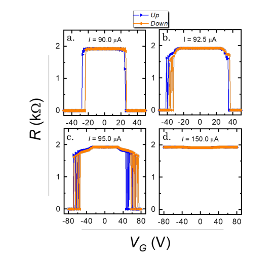
We also study electric field-induced switching of the device by applying different bias currents (90 A, 92.5 A, 95 A and 150 A) as shown in Fig. 3. The back-gate voltage was scanned for both upward (negative to positive) and downward (positive to negative) directions. While we are successfully and consistently, able to drive the system from superconducting to normal state and vice versa, we observe slight hysteresis with gate voltage sweeps as it approaches the transition voltage. With increase in the bias current, the gate voltage required for the transition is higher and the hysteresis becomes more prominent. This could arise as a consequence of charge pinning due to surface inhomogeneities in the thin film. The range over which the quasi-normal state exists broadens with increase in the bias current which may be attributed to inhomogeneous superconducting state at higher currents or intrinsic thermal excitation in the sample, and not due to phase dynamics in the superconductor. Such scaling of the area under the hysteresis curve with bias current makes our devices a potential candidate for cryogenic memory systems 20, 47. However the hysteresis may weaken in thinner films 48. When the bias current is set to a relatively large value of 150 A, the system does not achieve the superconducting state [Fig. 3(d)] within the limits of gate voltage allowed by the SiO2 dielectric.
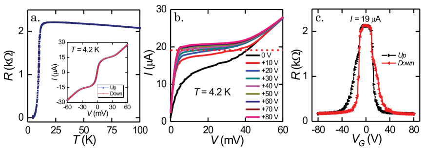
In order to examine the dependence of gating effect on the bridge dimensions and probe the device scalability to nano-regime, we now present results for the NB device with thickness nm (). Here, the aspect ratio was kept the same as that of the B. The resistance versus temperature curve in Fig. 4(a) shows a superconducting transition close to 12 K. However, the I-V characteristics show an additional normal metal behavior with finite resistance at 4.2 K [inset of Fig. 4(a)]. This appears to be the result of the edge disorder caused by Ar ion milling and the concomitant degradation of the nanowire causing a small drop in the 111We expect a sharper I-V characteristic at lower temperatures.. Nevertheless, in these NBs we observe a transition in Ic-like feature with gate bias similar to that of the B device discussed previously. On biasing with a constant current of 10 A and scanning the gate voltage, the NB recovers the superconducting state with a much broader hysteresis [Fig. 4(c)] possibly due to increased charge pinning effects. The in this case is nearly 1400%, which is extremely large but finite since the NB does not transition to a completely superconducting state at 4.2 K. We further note the absence of re-trapping currents 49 in all our devices, as seen via I-V characteristics i.e., symmetric in both forward and backward sweeps [Fig. 1 (c) and Fig. 4 (a)]. This observation is in contrast with previous works 20, 21, 26 and suggests the role of symmetric flux pinning edges.
Our experiments on both B and NB devices demonstrate a robust coupling of to gate-voltage exhibiting an infinite (large) in B (NB). Despite the drop in the NB on account of additional disorder, the qualitative effects reported herein remain the same as for the B thereby demonstrating their scalability for technological applications. Furthermore, the larger hysteresis in the NB should be beneficial for cryogenic memory devices. The gate voltage required to control the superconductor-normal state transition can be brought down significantly, by engineering the oxide layer thickness, to values comparable with the contemporary silicon technology. Finally, we note that similar measurements, presented in the supplementary information on 5 different devices with the same aspect ratio find essentially the same effects as discussed above.
Mechanism and discussion.— We now discuss a plausible mechanism for the observed enhancement in the . Depending on the sample details, such as physical dimensions 40, 41, 50, grains and so on, can be determined by a variety of processes such as critical pair-breaking 51, 52, 41, superconducting weak links 53, an intrinsic proximity effect 54, and surface vortex (flux) nucleation and flow 29, 30, 32. For a homogeneous type II superconductor with larger than or comparable to , it becomes energetically favorable for vortices nucleating at one edge to move across to the other at large enough currents. This instability of the vortex system then determines the 29, 30, 32, 53, 33, 34, 35 and has been the basis for understanding experiments including magnetic field induced enhancement in of bent superconductors 34.
Working under the assumption that the vortex instability mechanism discussed above determines the critical current in our films, an applied gate voltage can influence by changing the vortex surface barrier 29, 31. This appears consistent with two key features. First, our experimental observation that although is affected, critical temperature remains unaltered. A change in vortex surface barrier should not alter critical temperature. Second, the expectation that electric field is screened over atomic length scales in our high-carrier density superconductor 16. The gate voltage, therefore, drops largely over the interfaces causing strong interfacial electric fields. The latter should give rise to an interfacial Rashba spin-orbit interaction (SOI) parameterized by . We hypothesize that the ensuing interfacial SOI contributes an amount to the vortex surface barrier and discuss its origin further in the supplementary information. The vortex surface barrier, and thus the change in critical current, is therefore bipolar. In this manner, we are able to explain all the key features of our experiments with the caveat that our reasonable sounding hypotheses need to be examined via further theoretical and experimental analyses.
In our considerations above, we have assumed a homogeneous superconducting state consistent with existing experimental evidence for samples similar to ours 36. Finally, a possible role of magnetic impurities in determining the electric-field-induced vortex pinning in our devices cannot be ruled out 55. As detailed in the supplementary information, we have also observed similar gating effects in NbN/GdN bilayer films, where the ferromagnetic GdN layer may play a role via exchange-coupling to the superconducting NbN layer.
4 Conclusion
We have demonstrated gate-voltage-induced enhancement by up to in of NbN-based superconducting bridges. We have put forward a qualitative plausible model that explains our experiments in terms of gate-voltage-controlled surface pinning of vortices. Capitalizing on this voltage control, we demonstrate infinite electroresistance and hysteretic resistance variation in our devices making them promising candidates for logic and memory applications. Our work thus provides fundamental new insights into the field-effect in superconductors, paving the way for even larger voltage-controlled enhancement of superconducting properties, and developing novel low-dissipation computing paradigms.
Authors thank A. K. Saydjari, Prof. Jacobo Santamaria, Prof. Carlos Leon, Morten Amundsen, and Marius Kalleberg Hope for fruitful discussions. M.R. was supported by the Marie Skłodowska-Curie grant agreement EuSuper No. 796603 under the European Union’s Horizon 2020 research and innovation program. D.S. was supported by CIQM-NSF DMR-1231319, NSF Grant DMR1700137 and ONR Grant N00014-16-1-2657. Research at MIT was supported by NSF Grant DMR1700137, ONR Grant N00014-16-1-2657 and ARO grant W911NF1920041. A.K. acknowledges financial support from the Research Council of Norway through its Centers of Excellence funding scheme, project 262633, “QuSpin”. G.V. was supported by ARO grant W911NF1920041, Brazilian agencies CAPES (Gilvania Vilela/POS-DOC-88881.120327/2016-01), FACEPE (APQ-0565-1.05/14), CNPq and UPE (PFA/PROGRAD/UPE 04/2017). M.G.H., J.L.M. and N.M.N. were supported by Spanish MICIN grants MAT2017-87134- C02 and MAT2017-84496-R.
The Supporting Information is available free of charge on the ACS Publications website at DOI: XXXX. The SI contains results of measurements on additional devices of NbN and NbN/GdN bilayers; and further details of the proposed theoretical model for the mechanism.
References
- Bonfiglioli et al. 1956 Bonfiglioli, G.; Coen, E.; Malvano, R. Modulation of Conductivity by Surface Charges in Metals. Phys. Rev. 1956, 101, 1281–1284
- Bonfiglioli and Malvano 1959 Bonfiglioli, G.; Malvano, R. Surface States in Metals. Phys. Rev. 1959, 115, 330–335
- Glover and Sherrill 1960 Glover, R. E.; Sherrill, M. D. Changes in Superconducting Critical Temperature Produced by Electrostatic Charging. Phys. Rev. Lett. 1960, 5, 248–250
- Ahn et al. 2003 Ahn, C. H.; Triscone, J.-M.; Mannhart, J. Electric field effect in correlated oxide systems. Nature 2003, 424, 1015
- Xi et al. 1992 Xi, X. X.; Doughty, C.; Walkenhorst, A.; Kwon, C.; Li, Q.; Venkatesan, T. Effects of field-induced hole-density modulation on normal-state and superconducting transport in YBa2Cu3O7-x. Phys. Rev. Lett. 1992, 68, 1240–1243
- Frey et al. 1995 Frey, T.; Mannhart, J.; Bednorz, J. G.; Williams, E. J. Mechanism of the electric-field effect in the high- cuprates. Phys. Rev. B 1995, 51, 3257–3260
- Sajadi et al. 2018 Sajadi, E.; Palomaki, T.; Fei, Z.; Zhao, W.; Bement, P.; Olsen, C.; Luescher, S.; Xu, X.; Folk, J. A.; Cobden, D. H. Gate-induced superconductivity in a monolayer topological insulator. Science 2018, 362, 922–925
- Costanzo et al. 2016 Costanzo, D.; Jo, S.; Berger, H.; Morpurgo, A. F. Gate-induced superconductivity in atomically thin MoS2 crystals. Nature Nanotechnology 2016, 11, 339–344
- Hanzawa et al. 2016 Hanzawa, K.; Sato, H.; Hiramatsu, H.; Kamiya, T.; Hosono, H. Electric field-induced superconducting transition of insulating FeSe thin film at 35 K. Proceedings of the National Academy of Sciences 2016, 113, 3986–3990
- Wang et al. 2008 Wang, J.; Ma, X.-C.; Lu, L.; Jin, A.-Z.; Gu, C.-Z.; Xie, X. C.; Jia, J.-F.; Chen, X.; Xue, Q.-K. Anomalous magnetoresistance oscillations and enhanced superconductivity in single-crystal Pb nanobelts. Applied Physics Letters 2008, 92, 233119
- Giazotto 2015 Giazotto, F. A boost for quantum computing. Nat. Phys. 2015, 11, 527–528
- Linder and Robinson 2015 Linder, J.; Robinson, J. W. A. Superconducting spintronics. Nat. Phys. 2015, 11, 307–315
- Moraru et al. 2006 Moraru, I. C.; Pratt, W. P.; Birge, N. O. Magnetization-Dependent Shift in Ferromagnet/Superconductor/Ferromagnet Trilayers with a Strong Ferromagnet. Phys. Rev. Lett. 2006, 96, 037004
- Khaire et al. 2009 Khaire, T. S.; Pratt, W. P.; Birge, N. O. Critical current behavior in Josephson junctions with the weak ferromagnet PdNi. Phys. Rev. B 2009, 79, 094523
- Bergeret et al. 2018 Bergeret, F. S.; Silaev, M.; Virtanen, P.; Heikkilä, T. T. Colloquium: Nonequilibrium effects in superconductors with a spin-splitting field. Rev. Mod. Phys. 2018, 90, 041001
- Lipavský et al. 2010 Lipavský, P.; Koláček, J.; Morawetz, K. In Nanoscience and Engineering in Superconductivity; Moshchalkov, V., Woerdenweber, R., Lang, W., Eds.; Springer Berlin Heidelberg: Berlin, Heidelberg, 2010; pp 281–297
- Cavalleri 2018 Cavalleri, A. Photo-induced superconductivity. Contemp. Phys. 2018, 59, 31–46
- Demsar 2020 Demsar, J. Non-equilibrium Phenomena in Superconductors Probed by Femtosecond Time-Domain Spectroscopy. Journal of Low Temperature Physics 2020, xx, xx
- London and London 1935 London, F.; London, H. Supraleitung und diamagnetismus. Physica 1935, 2, 341 – 354
- De Simoni et al. 2018 De Simoni, G.; Paolucci, F.; Solinas, P.; Strambini, E.; Giazotto, F. Metallic supercurrent field-effect transistor. Nat. Nanotechnol. 2018, 13, 802–805
- De Simoni et al. 2019 De Simoni, G.; Paolucci, F.; Puglia, C.; Giazotto, F. Josephson Field-Effect Transistors Based on All-Metallic Al/Cu/Al Proximity Nanojunctions. ACS Nano 2019, 13, 7871–7876
- De Simoni et al. 2020 De Simoni, G.; Puglia, C.; Giazotto, F. Niobium Dayem nano-bridge Josephson gate-controlled transistors. Applied Physics Letters 2020, 116, 242601
- Puglia et al. 2020 Puglia, C.; De Simoni, G.; Ligato, N.; Giazotto, F. Vanadium gate-controlled Josephson half-wave nanorectifier. Appl. Phys. Lett. 2020, 116, 252601
- Erik et al. 2018 Erik, P.; Davide, R.; Gonnelli, R. S.; Dario, D. Anomalous screening of an electrostatic field at the surface of niobium nitride. Appl. Surf. Sci. 2018, 461, 17 – 22, 5th Progress in Applied Surface, Interface and Thin Film Science and Solar Renewable Energy News
- Rocci et al. 2020 Rocci, M.; De Simoni, G.; Puglia, C.; Esposti, D. D.; Strambini, E.; Zannier, V.; Sorba, L.; Giazotto, F. Gate-Controlled Suspended Titanium Nanobridge Supercurrent Transistor. ACS Nano 2020, xx, xx, Just Accepted
- Paolucci et al. 2018 Paolucci, F.; De Simoni, G.; Strambini, E.; Solinas, P.; Giazotto, F. Ultra-Efficient Superconducting Dayem Bridge Field-Effect Transistor. Nano Letters 2018, 18, 4195–4199
- Alegria et al. 2020 Alegria, L. D.; Bøttcher, C. G.; Saydjari, A. K.; Pierce, A. T.; Lee, S. H.; Harvey, S. P.; Vool, U.; Yacoby, A. High-Energy Quasiparticle Injection in Mesoscopic Superconductors. 2020, 2005.00584, arXiv, https://arxiv.org/abs/2005.00584 (accessed 2020–06–08)
- Ritter et al. 2020 Ritter, M. F.; Fuhrer, A.; Haxell, D. Z.; Hart, S.; Gumann, P.; Riel, H.; Nichele, F. A superconducting switch actuated by injection of high energy electrons. 2020, 2005.00462, arXiv, https://arxiv.org/abs/2005.00462 (accessed 2020–06–08)
- Shmidt 1970 Shmidt, V. V. Critical Currents in Superconductors. Sov. Phys. Uspekhi 1970, 13, 408–409
- Shmidt 1970 Shmidt, V. V. The Critical Current in Superconducting Films. Sov. Phys. JETP 1970, 30, 1137
- Bean and Livingston 1964 Bean, C. P.; Livingston, J. D. Surface Barrier in Type-II Superconductors. Phys. Rev. Lett. 1964, 12, 14–16
- Aslamazov and Larkin 1975 Aslamazov, L. G.; Larkin, A. I. Josephson effect in wide superconducting bridges. Sov. Phys. JETP 1975, 41, 381
- Mawatari and Yamafuji 1994 Mawatari, Y.; Yamafuji, K. Critical current density in thin films due to the surface barrier. Physica C: Superconductivity 1994, 228, 336 – 350
- Ilin et al. 2014 Ilin, K.; Henrich, D.; Luck, Y.; Liang, Y.; Siegel, M.; Vodolazov, D. Y. Critical current of Nb, NbN, and TaN thin-film bridges with and without geometrical nonuniformities in a magnetic field. Phys. Rev. B 2014, 89, 184511
- Clem and Berggren 2011 Clem, J. R.; Berggren, K. K. Geometry-dependent critical currents in superconducting nanocircuits. Phys. Rev. B 2011, 84, 174510
- Romestain et al. 2004 Romestain, R.; Delaet, B.; Renaud-Goud, P.; Wang, I.; Jorel, C.; Villegier, J.-C.; Poizat, J.-P. Fabrication of a superconducting niobium nitride hot electron bolometer for single-photon counting. New J. Phys. 2004, 6, 129–129
- Tinkham 2004 Tinkham, M. Introduction to Superconductivity; Dover Publications, INC., New York, 2004
- Komenou et al. 1968 Komenou, K.; Yamashita, T.; Onodera, Y. Energy gap measurement of niobium nitride. Phys. Lett. A 1968, 28, 335 – 336
- Chockalingam et al. 2008 Chockalingam, S. P.; Chand, M.; Jesudasan, J.; Tripathi, V.; Raychaudhuri, P. Superconducting properties and Hall effect of epitaxial NbN thin films. Phys. Rev. B 2008, 77, 214503
- Pearl 1964 Pearl, J. Current Distribution in Superconducting Films Carrying Quantized Fluxoids. Appl. Phys. Lett. 1964, 5, 65–66
- Romijn et al. 1982 Romijn, J.; Klapwijk, T. M.; Renne, M. J.; Mooij, J. E. Critical pair-breaking current in superconducting aluminum strips far below . Phys. Rev. B 1982, 26, 3648–3655
- Moodera et al. 1995 Moodera, J. S.; Kinder, L. R.; Wong, T. M.; Meservey, R. Large Magnetoresistance at Room Temperature in Ferromagnetic Thin Film Tunnel Junctions. Phys. Rev. Lett. 1995, 74, 3273–3276
- Moodera et al. 1999 Moodera, J. S.; Nassar, J.; Mathon, G. Spin-tuneling in ferromagnetic junctions. Annu. Rev. Mater. Sci. 1999, 29, 381–432
- Žutić et al. 2004 Žutić, I.; Fabian, J.; Das Sarma, S. Spintronics: Fundamentals and applications. Rev. Mod. Phys. 2004, 76, 323–410
- Fert 2008 Fert, A. Nobel Lecture: Origin, development, and future of spintronics. Rev. Mod. Phys. 2008, 80, 1517–1530
- Giazotto et al. 2006 Giazotto, F.; Heikkilä, T. T.; Luukanen, A.; Savin, A. M.; Pekola, J. P. Opportunities for mesoscopics in thermometry and refrigeration: Physics and applications. Rev. Mod. Phys. 2006, 78, 217–274
- Gingrich et al. 2016 Gingrich, E. C.; Niedzielski, B. M.; Glick, J. A.; Wang, Y.; Miller, D. L.; Loloee, R.; Pratt Jr, W. P.; Birge, N. O. Controllable 0-p Josephson junctions containing a ferromagnetic spin valve. Nat. Phys. 2016, 12, 564–567
- Tinkham et al. 2003 Tinkham, M.; Free, J. U.; Lau, C. N.; Markovic, N. Hysteretic curves of superconducting nanowires. Phys. Rev. B 2003, 68, 134515
- Courtois et al. 2008 Courtois, H.; Meschke, M.; Peltonen, J. T.; Pekola, J. P. Origin of hysteresis in a proximity Josephson junction. Phys. Rev. lett. 2008, 101, 067002
- Korneeva et al. 2018 Korneeva, Y. P.; Vodolazov, D. Y.; Semenov, A. V.; Florya, I. N.; Simonov, N.; Baeva, E.; Korneev, A. A.; Goltsman, G. N.; Klapwijk, T. M. Optical Single-Photon Detection in Micrometer-Scale NbN Bridges. Phys. Rev. Appl. 2018, 9, 064037
- Bardeen 1962 Bardeen, J. Critical Fields and Currents in Superconductors. Rev. Mod. Phys. 1962, 34, 667–681
- De Gennes 1999 De Gennes, P. G. Superconductivity of Metals and Alloys; Advanced book classics; Perseus: Cambridge, MA, 1999
- Likharev 1979 Likharev, K. K. Superconducting weak links. Rev. Mod. Phys. 1979, 51, 101–159
- Charaev et al. 2017 Charaev, I.; Silbernagel, T.; Bachowsky, B.; Kuzmin, A.; Doerner, S.; Ilin, K.; Semenov, A.; Roditchev, D.; Vodolazov, D. Y.; Siegel, M. Proximity effect model of ultranarrow NbN strips. Phys. Rev. B 2017, 96, 184517
- Mironov and Buzdin 2017 Mironov, S.; Buzdin, A. Spontaneous Currents in Superconducting Systems with Strong Spin-Orbit Coupling. Phys. Rev. Lett. 2017, 118, 077001