Dielectric nano-antennas for strain engineering in atomically thin two-dimensional semiconductors
Abstract
Atomically thin two-dimensional semiconducting transition metal dichalcogenides (TMDs) can withstand large levels of strain before their irreversible damage occurs. This unique property offers a promising route for control of the optical and electronic properties of TMDs, for instance by depositing them on nano-structured surfaces, where position-dependent strain can be produced on the nano-scale. Here, we demonstrate strain-induced modifications of the optical properties of mono- and bilayer TMD WSe2 placed on photonic nano-antennas made from gallium phosphide (GaP). Photoluminescence (PL) from the strained areas of the TMD layer is enhanced owing to the efficient coupling with the confined optical mode of the nano-antenna. Thus, by following the shift of the PL peak, we deduce the changes in the strain in WSe2 deposited on the nano-antennas of different radii. In agreement with the presented theory, strain up to is observed for WSe2 monolayers. We also estimate that strain is achieved in bilayers, accompanied with the emergence of a direct bandgap in this normally indirect-bandgap semiconductor. At cryogenic temperatures, we find evidence of the exciton confinement in the most strained nano-scale parts of the WSe2 layers, as also predicted by our theoretical model. Our results, of direct relevance for both dielectric and plasmonic nano-antennas, show that strain in atomically thin semiconductors can be used as an additional parameter for engineering light-matter interaction in nano-photonic devices.
keywords:
transition metal dichalcogenides, dielectric nanoantennas, exciton, strain engineering, photoluminescenceChair in Hybrid Nanosystems, Nanoinstitute Münich, Faculty of Physics, Ludwig-Maximilians-Universität München, 80539 Münich, Germany
![[Uncaptioned image]](/html/2002.04278/assets/FigTOC.png)
Control over lattice distortions in semiconductors, or strain-engineering, offers valuable tools for tailoring their electronic and optical properties. The exceptional flexibility of atomically thin two-dimensional (2D) crystals 1 has opened the way to employ mechanical deformation for engineering their physical properties 2, 3, 4, 5, 6, 7, and has made them promising for applications in flexible electronics 8, 9. Among 2D semiconductors, the family of transition metal dichalcogenides 10 has shown attractive properties including an indirect-to-direct bandgap transition in monolayers 11, 12, tightly bound excitons 13 and coupling between the spin and valley degrees of freedom 14. Single layers of TMDs, only three atoms thick, have been observed to withstand large strain levels (10%)15 before fracture, offering a unique possibility to engineer their electronic band structure using strain 16, 17, 18, 19, 20. This approach has been successfully applied for modifying their optical properties 21, 22, 23, 24, 25, 26, tuning carrier mobilities 27 and controlling the charge transport 28, 29. Furthermore, spatial variation of the strain in TMD layers, occurring due to imperfections of fabrication methods or introduced intentionally, translates into a position dependent bandgap 30, 31. This was shown to result in periodically modulated optical properties in monolayer MoS2 placed on pre-patterned substrates 32, as well as to give rise to funnelling of excitons into the areas with a larger tensile strain 33, 34, where the lowest exciton energy is achieved. Finally, in mono- and bi-layer WSe2 and WS2 placed on silica or polymer nano-pillars, single photon emitting defects were readily observed, whose origin was thus linked with the strain induced in the few-layer semiconductor 35, 36.
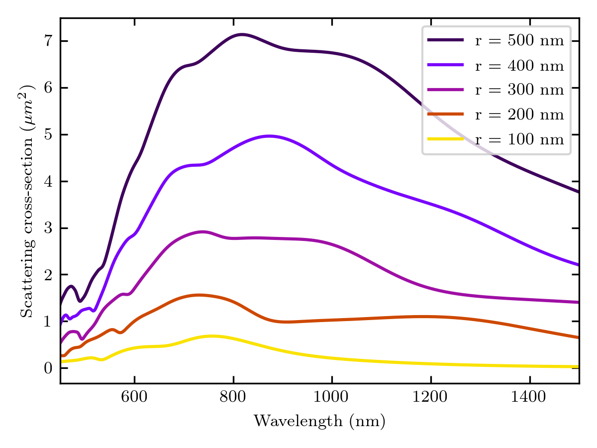
While initial demonstrations of strained 2D semiconductors in electronic devices have been reported 27, 37, the use of strain to control the optical properties of TMDs in nano-photonic systems has been largely unexplored 38. One of the approaches to engineer light-matter interaction relies on the use of nano-antennas 39, 40, 41, which can confine light in volumes below the diffraction limit 42. The strong confinement of the electric field at the hot-spots of the nano-antenna, enhances the light-matter interaction for the emitters positioned within the volume of its optical mode 43, 44, 45. While these phenomena have been extensively studied for surface plasmons in metals 46, 47, recently high-refractive-index dielectric nano-photonic structures 48 have rapidly gained attention as they offer low losses 49, 50 and both electric and magnetic Mie-type optical resonances 51. Recent reports of dielectric nano-antennas interfaced with 2D TMDs showed modified PL directionality in monolayer MoS2 coupled to silicon nano-rods 52, as well as strong PL and Raman signal enhancement for WSe2 placed on top of GaP dimer nano-pillars 43. In this work, we investigate the role of strain in the latter case of the dimer structures. Compared with a more trivial case of single pillars, which can also be used to provide local strain 36, 35, the dimer nano-pillars provide stronger light-matter interaction with more interesting photonic properties 43, thus motivating our study.

Contrary to previous approaches employing bending apparatuses 21, piezoelectric substrates 53 or relying on the difference of the thermal expansion coefficients 54, 55, here we demonstrate that dimer nano-antennas can be used to strain a 2D semiconducting layer, while at the same time the PL from the strained material is enhanced via the coupling with the optical mode of the nano-antenna 43. We study both experimentally and theoretically monolayers (1L) and bilayers (2L) of TMD WSe2 transferred on closely spaced (100 nm) pairs of nano-pillars, referred to as dimers 56, 43 below (see Figs.1a-d). The co-location between WSe2 tensile deformation and the maximum of the near-field enhancement of the antenna at the edges of the top surface of the pillars (Fig.1b-e), allows clear observation of the strain-induced band structure modifications in PL. We demonstrate a dependence of the amount of strain induced in the TMD layer by nano-antennas of different radii. With this approach we observe the tuning of the intralayer exciton in monolayer WSe2 exceeding 50 meV, corresponding to the uniaxial tensile strain up to 57. These findings are supported by our model based on the continuum-mechanical plate theory approach 58, 59, which we use to calculate the strain distribution in 1L and 2L-WSe2 placed on the nano-antennas. Using this theory we predict higher strain in the bilayers than in monolayers placed on the nano-antennas of the same radius. Tensile strain is calculated for 2L-WSe2 placed on the nano-antenna with nm, for which we experimentally observe abrupt changes in the PL spectrum consistent with the transition to the direct bandgap. From the calculated topography model, we deduce the position-dependent band structure induced in the WSe2 and predict occurrence of strain-induced potential wells at the nano-pillar edges, which can trap the excitons. This behaviour is confirmed in the cryogenic PL measurements of 2L-WSe2, which exhibits localization of the excitonic PL, consistent with the predicted potential shape. Further to demonstrating tuning of strain in TMDs using all-dielectric nano-antennas of various dimensions, our findings have direct relevance to TMDs coupled to plasmonic structures, where similarly both the strain and the enhanced optical fields may be co-located 60, 61.
Results
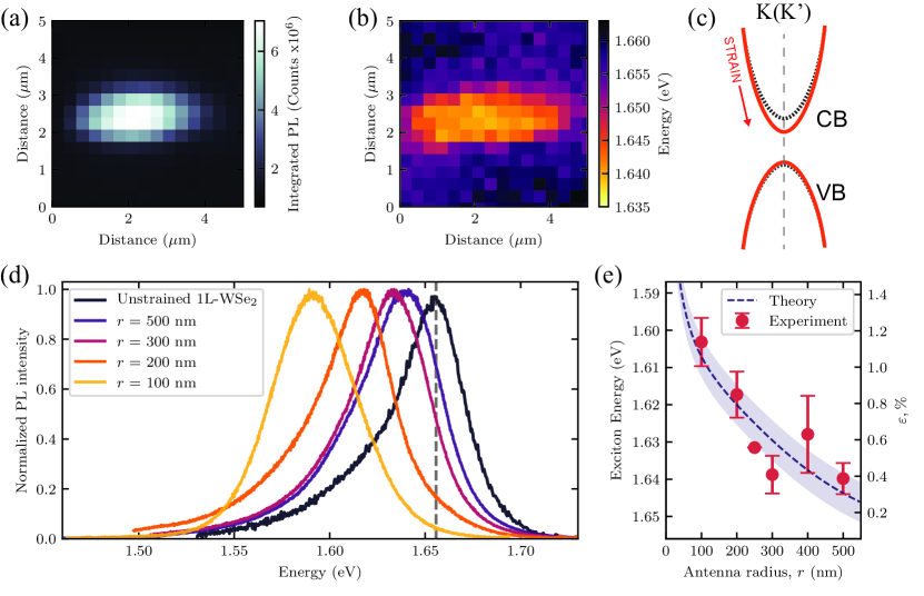
Strained WSe2 coupled with GaP nano-antennas Fig.1a shows an electron microscopy image of the top view of a GaP dimer nano-antenna with an atomically thin WSe2 bilayer deposited on top. Owing to its elasticity, the thin semiconductor crystal stretches from the substrate up to the topmost edge of the nano-antenna, without compromising its integrity. Fig.1b shows a schematic diagram of a WSe2 monolayer (0.7 nm thick) transferred on top of a GaP dimer nano-antenna. We use nano-antennas with a height of 200 nm, a radius varying from 50 to 500 nm and a gap from 50-100 nm. Due to the height mismatch between the substrate and the top surface of the antenna, the WSe2 layer experiences a local compressive or tensile deformation, as shown in Fig.1b,e. The optical response of a dimer nano-antenna exhibits spectrally broad resonances 56, 43 (see calculated spectra in Supplementary Note I). Fig.1c shows the spatial intensity distribution of the scattered light of a nano-antenna illuminated with a planar wave at the top surface of a GaP dimer nano-antenna under unpolarized excitation. We present this scattered intensity as , where is the electric field in the scattered wave, and is the electric field of the plane wave illuminating the structure. Maxima of the field intensity are located at the edges of each nano-pillar and inside the gap region between them. The transferred 2D semiconductor layer stretches over the nano-structure, fully overlapping with the confined optical modes 43. An optical microscope image of 1L-WSe2 PL emission on top of a single GaP dimer nano-antenna, with nm and nm, is shown in Fig.1d (see Methods and Ref.62 for more details). In this image it is possible to resolve the spatial distribution of the PL signal which closely resembles that of the enhanced field in Fig.1c.
We describe the nano-scale distortions in the 2D layer with an approach based on the continuum-mechanical plate theory 58 by modelling the pressure experienced by the stretched semiconductor in the out-of-plane direction (see Supplementary Note II for the full description of the model). From the analytically calculated function for a single pillar, we interpolate to the low-symmetry dimer structure and calculate the spatial distribution of strain introduced in the stretched semiconductor crystal. The resulting strain topography for a 1L-WSe2 placed on top of a dimer nano-antenna is shown in Fig.1e. The tensile strain reaches its maximum at the topmost edge of each nano-pillar, at a height nm, co-located with the largest near-field enhancement produced by the underlying nano-antenna. The regions of compressive strain are located where the 2D layer touches the substrate, at , and inside the gap region between the pillars.
In what follows, we show that the co-location of the maximum of the confined optical mode and that of the tensile deformation in the 2D layer, allows us to directly probe the strain-induced band structure renormalization by monitoring the enhanced excitonic room temperature PL emission for both 1L and 2L-WSe2. At cryogenic temperature, we show the exciton PL localization in 2L-WSe2 in the regions of the largest tensile strain where the reduction of the exciton energy is the strongest, as predicted by our theoretical model.
Strain tuning in 1L-WSe2 coupled to GaP nano-antennas We studied the emission from the same nano-antenna shown in Fig.1 in a micro-PL setup at room temperature using PL mapping with a micron resolution (see Methods), as shown in Fig.2a. The sample is excited at 685 nm, below the absorption edge of GaP, and thus this light is only absorbed by the WSe2 layer. As expected, a large enhancement in the overall WSe2 PL intensity is correlated with the location of the nano-antenna. Note, that in contrast to Fig.1d, here the resolution is limited by the excitation spot size ( m). As shown in Fig.2b, we extract the peak maxima from the PL map in Fig.2a and observe a prominent red-shift of the intralayer exciton (also referred to as ’A exciton’) peak on the nano-antenna. This effect is expected from the reduction of the WSe2 bandgap under tensile strain. As schematically shown in Fig.2c, the direct optical transition in 1L-WSe2 is located at the K(K’) point of the Brillouin zone 12, 11. Under the increasing tensile strain, the bandgap is expected to reduce 25, 24 mainly due to the lowering of the conduction band minimum, as a consequence of the change in the electronic orbital overlap following the the changes in the atomic bond lengths and angles 18, 17, 20. Strain induced by underlying nano-structures has previously been measured using Raman enhancement in graphene on plasmonic nano-antennas63, 64. As we show in Supplementary Note III, we collected the Raman scattering signal from the strained 1L-WSe2 and observe a shift of the Raman peak, as expected for tensile strain 65.
From our theoretical description we have derived a dependence of the tensile strain maximum, located at the nano-pillar edges, on the nano-antenna size (see Supplementary Note II). We found that by reducing the nano-pillar radius an increased strain is introduced in the 2D layer. We confirm this trend experimentally in Fig.2d which shows the normalized 1L-WSe2 PL spectra for the TMD coupled to nano-antennas of different radii (see also Supplementary Note IV for raw PL spectra and more PL characterization data). For comparison we also show the PL spectrum for WSe2 on a planar GaP substrate, where the intralayer exciton peak is marked by a dashed line. When the nano-pillar radius is reduced, the larger red-shift in the exciton PL peak confirms that the semiconducting layer is experiencing an increased strain, as predicted by our model.
By using the previously experimentally observed gauge value for the WSe2 intralayer A exciton red-shift as a function of strain of meV/ 57, we extract the uniaxial tensile strain magnitude for WSe2 placed on the nano-antennas with different radii. As shown in Fig.2e, we find tensile strain values up to as the nano-antenna radius is reduced, comparable to the estimate from our theoretical model shown with the dashed line. There is a variation in the peak position measured on different pillars. This effect can be attributed to the non-uniform coverage of the antenna surface by the monolayer and from the local disorder introduced in the WSe2 layer for instance from wrinkles, contamination etc. Further variation may occur due to imperfections in fabrication of the nano-antennas. These effects are also responsible for additional broadening of the PL linewidth, which is otherwise expected to reduce in WSe2 monolayers under uniform strain 57.
Direct bandgap transition in 2L-WSe2 As schematically shown in Fig.3a, using the band-structure picture without excitonic effects, contrary to the monolayer case, a WSe2 bilayer is an indirect bandgap semiconductor. It exhibits two main recombination pathways at room temperature, a momentum direct (higher energy) and indirect (lower energy) transition, respectively involving the K and Q points of the conduction band 16. For unstrained 2L-WSe2 (black dashed line) the lowest energy transition is the phonon-assisted recombination between the conduction band minimum at the Q point and the valence band maximum at the K point. Under tensile strain (coloured lines in Fig.3a), similar to the monolayer case, the conduction band minimum at the K point exhibits a reduction in energy, leading to a transition from the indirect to direct bandgap in highly strained 2L-WSe2 65, 66. In previous reports, there were contrasting interpretations for the dependence of the Q valley energy on strain 65, 66. In Fig.3a we use the interpretation from Ref.66, thus assuming that the Q valley energy would reduce under the tensile strain. However, the tuning of the Q valley is found to be negligible in the range of strain investigated in our samples (see more detailed PL spectra analysis in Supplementary Note V). The bandgap behaviour is thus determined by the stronger shift of the K valley to lower energy under tensile strain. Note, that in the exciton picture, the behaviour described above will translate in the corresponding energy shifts of the momentum-bright K-K exciton and the momentum-dark Q-K exciton.

Fig.3b shows a room temperature PL spectrum for the unstrained 2L-WSe2 placed on a flat GaP substrate. In contrast to what found for the monolayer, the bilayer exhibits a broad spectrum composed of two peaks, attributed to the momentum indirect eV and momentum direct eV exciton transitions 16, 67. The corresponding individual peaks obtained from the fitting of the PL spectrum are shown with dashed lines in Fig.3b.
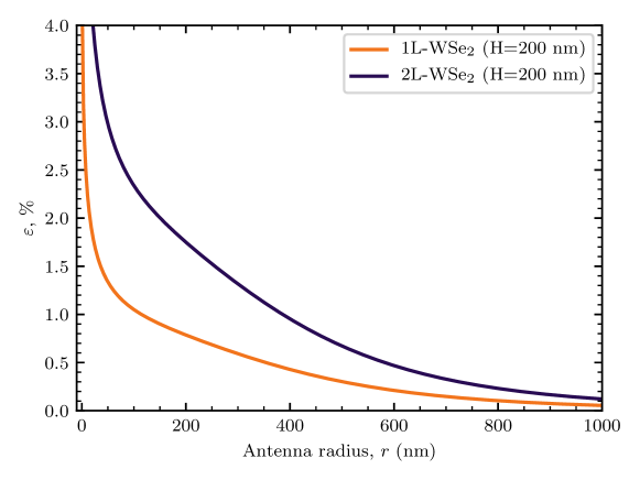
In analogy with the analysis carried out for WSe2 monolayers, we collected the PL emission of the strained bilayer placed on top of the nano-antennas with different radii. The normalized PL spectra measured for the nano-antennas of different radii are shown in Fig.3c (see also Supplementary Fig.S5). For the strained WSe2 bilayer, the presence of two transitions leads to a less evident strain-induced shift of the PL spectra. However, by comparing the spectral shape to that of the unstrained case we observe that, as the nano-antenna radius is reduced, the higher energy side of the spectrum shows a consistent shift to lower energies, following an abrupt change of the PL spectrum from that on the flat GaP (dashed red line) to the spectrum measured on a pillar with nm (yellow). The shift is accompanied with a reduction of the linewidth related to the reduction of the exciton-phonon coupling in WSe2 under strain 57. We attribute the red-shift under increasing tensile strain to the reduction in energy of the transition, as we observed for the monolayer case. Moreover, the PL lineshape exhibits a further abrupt change when the 2L-WSe2 is deposited on top of a GaP dimer nano-antenna with nm. This spectral shape and peak position resemble those reported in Ref.65, 66 where they were attributed to a transition to the direct bandgap, occurring due to the red-shift of the high-energy peak at (see also Supplementary Note V). Our theoretical model predicts strain values for 2L-WSe2 placed on the nano-antennas with nm (see Supplementary Fig.S2). This value is comparable with the reported threshold for the direct bandgap transition observed in WSe2 bilayers 66.
Note, that for the pillars of the same radius, a higher strain is introduced in the bilayer compared with a monolayer, due to the larger rigidity and larger mass of the former. Thus, a stronger bandgap tuning is observed in a bilayer. A similar effect has been reported in suspended 1L and 2L-MoS2 under the strain introduced by an AFM probe 28.
Exciton confinement in the strain-induced potential Controlled nano-scale deformations observed in Fig.1-3 allow the control of exciton motion in 2D semiconductors by means of band structure modification 33, 34. For WSe2, the application of tensile strain results in the increase of the valence band edge energy and reduction of the conduction band edge energy at the K point. This effect leads to so-called exciton funnelling 58, 33, where a strain gradient directs the excitonic population towards the strain-induced potential well. This effect has been proposed to play a role in the population of the single photon emitting centres in WSe2 at cryogenic temperatures 36, 35. In order to elucidate the role of the confinement produced by the strain, we probed the spatial dependence of the PL emission of 2L-WSe2. The experiments are carried out at a cryogenic temperature of 4 K where the effect of the strain-induced confinement is most pronounced.
From our strain topography model, it is possible to calculate the strain-induced potential for the case of the dimer structures (see Supplementary Note II). We find that the strain-induced potential wells are located at the nano-pillar edges, where the tensile strain is maximized 33, 58. When strain becomes compressive, i.e. where the layer touches the substrate, we observe the presence of potential barriers due to the opposite shift of the band edges, leading to an increase of the bandgap energy. Fig.4a shows the profile of the strained 2L-WSe2 (dashed line) on top of a dimer nano-antenna with nm (red squares). The TMD profile shown in the top panel is calculated for a cross section along the axis (as defined in Fig.1e), where is the centre of the dimer gap. We correlate the local deformation with the changes in the energy of the conduction band minimum (), calculated numerically for the K valley (see the bottom panel in Fig.4a and Supplementary Note II for details). The minima of are localized at the nano-pillar edges, resulting in a confinement potential wells (shaded areas). For WSe2 the valence band maximum, , exhibits an increase (decrease) in case of tensile (compressive) strain, also resulting in a confinement for holes, although this effect is weaker compared to conduction band electrons. In such a potential landscape, the exciton population will accumulate in the potential wells at the nano-pillar edges.
Fig.4b shows a reference PL spectrum of 2L-WSe2 collected at 4 K on the planar GaP (black) and on a dimer nano-antenna with nm (orange). The low temperature PL of 2L-WSe2 is dominated by the low energy broad band between 1.5 and 1.6 eV, relatively weakly dependent on the strain induced by the dimer. Overall the spectrum is characterized by the non-trivial combination of PL from bright and dark states, phonon replicas 68 and emission of various localized states 69. The only part of this broad band that consistently shows dependence on the strain induced by the pillars is the lower side of the spectrum between 1.5 and 1.55 eV, which exhibits higher intensity in the strained WSe2. One of the reasons for such behaviour could be that the PL in the range 1.55-1.6 eV may originate from the transitions involving the valley in the conduction band 68, which is weakly sensitive to the strain. On the other hand, we may conclude that the PL in the spectral range of 1.5 to 1.55 eV may arise from the localized exciton states, with the energies following the overall reduction in the direct bandgap by about 45 meV (see details below), or perhaps the optical transitions involving the valley in the conduction band. However, the complete understanding of this behaviour requires elaborate theory for the optical transitions in bilayer WSe2 and is beyond the scope of this work.
Despite the very low PL intensity, as expected at low in WSe2, we are still able to observe the momentum-direct exciton transition for the unstrained WSe2 on the planar GaP at 1.7 eV (inset Fig.4b). As expected for the direct transition, in the strained WSe2 placed on the nano-antenna, the corresponding exciton peak is observed approximately 45 meV lower at 1.655 eV (denoted ). From this energy red-shift we estimate a tensile strain value of , consistent with our theoretical model predictions. As we show in Supplementary Note VI, we observe a similar red-shift in the cryogenic PL of the strained 1L-WSe2 exciton, also in agreement with our model.

Fig.4c shows a one-dimensional hyper-spectral PL image of 2L-WSe2 placed on top of four GaP nano-antennas having nm and the gap size varying between 100 and 150 nm from left to right. The PL image is measured by scanning the collection and excitation spot along the nano-antenna -axis (see Fig.1e for the axis definition), while on the vertical axis of the figure we report the spectral distribution of the collected PL emission. The increased PL intensity corresponds to the enhanced 2L-WSe2 PL on top of the dimer nano-antennas, with a negligible signal collected on the flat GaP (dark areas in between).
In the right panel of Fig.4c we zoom in on the direct exciton PL emission in the strained WSe2 at around 1.655 eV. The exciton PL intensity exhibits a clear localization into two spatially separated maxima. Fig.4d shows the integrated intensity of the exciton PL (in black) clearly highlighting this behaviour. Such two-peaked distribution is also reproduced to some degree for the lowest part of the PL spectrum below 1.52 eV. This is a consequence of the sensitivity of this part of the spectrum to the induced strain as observed in Fig.4b. We conclude that for the two types of states, exciton relaxation into the strain-induced potential minima is significant.
Discussion
In summary, we have demonstrated strain-tuning of the electronic band structure in 2D semiconductor WSe2 by placing the atomic mono- and bilayers on pre-patterned dielectric nano-antennas. Because of the efficient coupling with the optical mode confined at the surface of the nano-antenna, the PL of the strained WSe2 is enhanced. It can thus be clearly detected with negligible contribution from the PL of the unstrained material, that would normally mask the effect of strain, for example, in the case of the pillars made of SiO2 or polymers, which were employed previously to induce strain 36, 32. We therefore can clearly deduce the amount of induced strain from the red-shift in WSe2 PL spectra at room temperature in agreement with our theory. Moreover, we observe excitons confined into strain-induced potential wells at cryogenic temperature, the presence of which is also predicted by our theoretical model.
The results presented in this work open the way for the use of strain as an additional degree of freedom in engineering of the light-matter interaction in 2D materials, and could find applications for studying 2D excitons in confined potentials, relevant for positioning of strain-induced WSe2 quantum emitters36, 35, as well as for Bose-Einstein condensation of interlayer excitons in TMDs heterostructures70.
Additionally, our continuum-mechanical theoretical approach can be expanded to describe the strain distribution and resulting distortion potential for 2D TMDs coupled to a broad range of nano-structures including plasmonic nano-antennas. This opens the way for designing optically active nano-photonic platforms interfaced with strained 2D materials and their heterostructures, with prospects in photodetection, light emission and photovoltaic applications.
Methods
Sample fabrication The GaP nano-antennas are fabricated with a top-down lithography process, as described in Ref.56. The monolayers and bilayers of WSe2 were mechanically exfoliated from commercially available bulk crystal (HQGraphene) and the layer thickness identified via a PL imaging technique62. The 2D layers are transferred on top of the GaP nano-antennas in a home-built transfer setup, with an all-dry transfer technique71.
Optical spectroscopy The PL image used in Fig.1d is obtained in a commercial bright-field microscope (LV150N Nikon), with the technique described in Ref.62, where the white light source is used both to image the TMD layers and to excite its PL emission. A 550 nm short-pass filter is placed in the illumination beam path to remove the low energy side of the white light emission spectrum. A high numerical aperture objective (Nikon x100 NA=0.9) is used to direct the light on the sample and for collecting the reflected and emitted light. In the collection path a 600 nm long-pass filter rejects the white light source, while the PL image from the TMD layer is detected with a microscope camera (DS-Vi1, Nikon).
Room temperature optical spectroscopy is performed in a home built micro-PL setup in back reflection geometry. A diode laser with a wavelength of nm is used as the excitation source and directed into an infinity corrected objective (Mitutoyo 100x NA=0.7), allowing focussing in a 3 m spot. We use a laser power of 30 W. The sample is placed on a motorized stage (STANDA-8MTF) which allows the automated mapping of the sample surface. The emitted light is collected by the same objective and using free space (no optical fibers) is then coupled to a spectrometer (Princeton Instruments SP2750) equipped with a high-sensitivity liquid nitrogen cooled charge-coupled device (Princeton Instruments PyLoN).
For optical spectroscopy at cryogenic temperature T 4 K, the sample is placed into a microscope stick (attocube systems AG) with a cage structure and a window for optical access. The sample is placed onto piezoelectric nano-positioners (attocube ANP101 models). The cage structure is fitted into an aluminium tube and held under high-vacuum. The tube is then inserted in a liquid helium bath cryostat and an optical breadboard with a micro-PL setup is placed on top of the tube to carry out the optical analysis. PL spectra were excited with the same laser as for room temperature measurements with nm. The incident power was kept at 100 W, and the excitation spot with a diameter of 3 m was achieved. The light emitted by the sample is coupled to a single mode optical fibre and detected in the same spectrometer/CCD system employed for the room temperature spectroscopy.
Additional measurements at a cryogenic temperature of T10 K reported in the inset of Fig.4b were carried out in a He flow cryostat using the same setup as was employed for the room temperature PL measurements. The PL was excited with a 532 nm laser with 1 mW power and coupled via free space into the spectrometer.
L. S. and A. I. T. thank the financial support of the European Graphene Flagship Project under grant agreements 785219, and EPSRC grant EP/S030751/1. L. S., A. I. T., M. B. and G. B. thank the European Union’s Horizon 2020 research and innovation programme under ITN Spin-NANO Marie Sklodowska-Curie grant agreement no. 676108. P. G. Z. and A. I. T. thank the European Union’s Horizon 2020 research and innovation programme under ITN 4PHOTON Marie Sklodowska-Curie grant agreement no. 721394. A. G. and A. I. T. acknowledge funding by EPSRC grant EP/P026850/1. J. C., S. M., S. A. M., and R. S. acknowledge funding by EPSRC (EP/P033369 and EP/M013812). S. A. M. acknowledges the Lee-Lucas Chair in Physics and the Solar Energies go Hybrid (SolTech) programme.
Author contributions
L. S., A. I. T., S. A. M., R. S. conceived the idea of the experiment. L. S. and P. G. Z. fabricated WSe2 layers and transferred them on the GaP nano-antennas. L. S., P. G. Z. and A. G. carried out microscopy and optical spectroscopy measurements on WSe2. J. C. fabricated GaP nano-antennas. S. M., J. C. and R. S. designed GaP nano-antennas. L. S., P. G. Z., A. G. and A. I. T. analysed optical spectroscopy data. M. B. and G. B. developed the theory and carried out simulations for strained WSe2. G. B., S. A. M., R. S. and A. I. T. managed various aspects of the project. L. S., M. B. and A. I. T. wrote the manuscript with contributions from all co-authors. A. I. T. oversaw the whole project.
-
•
Optical resonances of GaP dimer nano-antennas; theoretical modelling of strain topography; Raman spectroscopy of strained 1L-WSe2, Raw PL spectra from strained WSe2; PL spectra for strained 2L-WSe2; Strain-induced exciton red-shift in 1L-WSe2 at cryogenic temperatures;
References
- Lee et al. 2008 Lee, C.; Wei, X.; Kysar, J. W.; Hone, J. Measurement of the Elastic Properties and Intrinsic Strength of Monolayer Graphene. Science (80-. ). 2008, 321, 385–388
- Guinea et al. 2010 Guinea, F.; Katsnelson, M. I.; Geim, A. K. Energy gaps and a zero-field quantum Hall effect in graphene by strain engineering. Nat. Phys. 2010, 6, 30–33
- Duerloo et al. 2012 Duerloo, K.-A. N.; Ong, M. T.; Reed, E. J. Intrinsic Piezoelectricity in Two-Dimensional Materials. J. Phys. Chem. Lett. 2012, 3, 2871–2876
- Wu et al. 2014 Wu, W.; Wang, L.; Li, Y.; Zhang, F.; Lin, L.; Niu, S.; Chenet, D.; Zhang, X.; Hao, Y.; Heinz, T. F.; Hone, J.; Wang, Z. L. Piezoelectricity of single-atomic-layer MoS2 for energy conversion and piezotronics. Nature 2014, 514, 470–474
- Roldán et al. 2015 Roldán, R.; Castellanos-Gomez, A.; Cappelluti, E.; Guinea, F. Strain engineering in semiconducting two-dimensional crystals. J. Phys. Condens. Matter 2015, 27, 313201
- Amorim et al. 2015 Amorim, B.; Cortijo, A.; De Juan, F.; Grushin, A. G.; Guinea, F.; Gutiérrez-Rubio, A.; Ochoa, H.; Parente, V.; Roldán, R.; San-Jose, P.; Schiefele, J.; Sturla, M.; Vozmediano, M. A. Novel effects of strains in graphene and other two dimensional materials. Phys. Rep. 2015, 617, 1–54
- Dai et al. 2019 Dai, Z.; Liu, L.; Zhang, Z. Strain Engineering of 2D Materials: Issues and Opportunities at the Interface. Adv. Mater. 2019, 1805417, 1805417
- Akinwande et al. 2014 Akinwande, D.; Petrone, N.; Hone, J. Two-dimensional flexible nanoelectronics. Nat. Commun. 2014, 5, 5678
- Mueller and Malic 2018 Mueller, T.; Malic, E. Exciton physics and device application of two-dimensional transition metal dichalcogenide semiconductors. npj 2D Mater. Appl. 2018, 2, 29
- Manzeli et al. 2017 Manzeli, S.; Ovchinnikov, D.; Pasquier, D.; Yazyev, O. V.; Kis, A. 2D transition metal dichalcogenides. Nat. Rev. Mater. 2017, 2
- Mak et al. 2010 Mak, K. F.; Lee, C.; Hone, J.; Shan, J.; Heinz, T. F. Atomically Thin MoS2 : A New Direct-Gap Semiconductor. Phys. Rev. Lett. 2010, 105, 136805
- Splendiani et al. 2010 Splendiani, A.; Sun, L.; Zhang, Y.; Li, T.; Kim, J.; Chim, C.-Y.; Galli, G.; Wang, F. Emerging Photoluminescence in Monolayer MoS2. Nano Lett. 2010, 10, 1271–1275
- Wang et al. 2018 Wang, G.; Chernikov, A.; Glazov, M. M.; Heinz, T. F.; Marie, X.; Amand, T.; Urbaszek, B. Colloquium : Excitons in atomically thin transition metal dichalcogenides. Rev. Mod. Phys. 2018, 90, 021001
- Xu et al. 2014 Xu, X.; Yao, W.; Xiao, D.; Heinz, T. F. Spin and pseudospins in layered transition metal dichalcogenides. Nat. Phys. 2014, 10, 343–350
- Bertolazzi et al. 2011 Bertolazzi, S.; Brivio, J.; Kis, A. Stretching and breaking of ultrathin MoS2. ACS Nano 2011, 5, 9703–9709
- Yun et al. 2012 Yun, W. S.; Han, S. W.; Hong, S. C.; Kim, I. G.; Lee, J. D. Thickness and strain effects on electronic structures of transition metal dichalcogenides: 2H-MX2 semiconductors (M=Mo,W;X=S,Se,Te). Phys. Rev. B 2012, 85, 033305
- Johari and Shenoy 2012 Johari, P.; Shenoy, V. B. Tuning the Electronic Properties of Semiconducting Transition Metal Dichalcogenides by Applying Mechanical Strains. ACS Nano 2012, 6, 5449–5456
- Chang et al. 2013 Chang, C.-H.; Fan, X.; Lin, S.-H.; Kuo, J.-L. Orbital analysis of electronic structure and phonon dispersion in MoS2, MoSe2, WS2 and WSe2 monolayers under strain. Phys. Rev. B 2013, 88, 195420
- Guzman and Strachan 2014 Guzman, D. M.; Strachan, A. Role of strain on electronic and mechanical response of semiconducting transition-metal dichalcogenide monolayers: An ab-initio study. J. Appl. Phys. 2014, 115, 243701
- Kormányos et al. 2015 Kormányos, A.; Burkard, G.; Gmitra, M.; Fabian, J.; Zólyomi, V.; Drummond, N. D.; Fal’ko, V. k · p theory for two-dimensional transition metal dichalcogenide semiconductors. 2D Mater. 2015, 2, 022001
- Conley et al. 2013 Conley, H. J.; Wang, B.; Ziegler, J. I.; Haglund, R. F.; Pantelides, S. T.; Bolotin, K. I. Bandgap Engineering of Strained Monolayer and Bilayer MoS2. Nano Lett. 2013, 13, 3626–3630
- Castellanos-Gomez et al. 2013 Castellanos-Gomez, A.; Roldán, R.; Cappelluti, E.; Buscema, M.; Guinea, F.; van der Zant, H. S. J.; Steele, G. A. Local Strain Engineering in Atomically Thin MoS2. Nano Lett. 2013, 13, 5361–5366
- Feierabend et al. 2017 Feierabend, M.; Morlet, A.; Berghäuser, G.; Malic, E. Impact of strain on the optical fingerprint of monolayer transition-metal dichalcogenides. Phys. Rev. B 2017, 96, 045425
- Aslan et al. 2018 Aslan, O. B.; Deng, M.; Heinz, T. F. Strain tuning of excitons in monolayer WSe2. Phys. Rev. B 2018, 98, 115308
- Schmidt et al. 2016 Schmidt, R.; Niehues, I.; Schneider, R.; Drüppel, M.; Deilmann, T.; Rohlfing, M.; de Vasconcellos, S. M.; Castellanos-Gomez, A.; Bratschitsch, R. Reversible uniaxial strain tuning in atomically thin WSe2. 2D Mater. 2016, 3, 021011
- Tedeschi et al. 2019 Tedeschi, D.; Blundo, E.; Felici, M.; Pettinari, G.; Liu, B.; Yildrim, T.; Petroni, E.; Zhang, C.; Zhu, Y.; Sennato, S.; Lu, Y.; Polimeni, A. Controlled Micro/Nanodome Formation in Proton-Irradiated Bulk Transition-Metal Dichalcogenides. Adv. Mater. 2019, 31, 1903795
- Liu et al. 2019 Liu, T.; Liu, S.; Tu, K.-H.; Schmidt, H.; Chu, L.; Xiang, D.; Martin, J.; Eda, G.; Ross, C. A.; Garaj, S. Crested two-dimensional transistors. Nat. Nanotechnol. 2019, 1, 1
- Manzeli et al. 2015 Manzeli, S.; Allain, A.; Ghadimi, A.; Kis, A. Piezoresistivity and Strain-induced Band Gap Tuning in Atomically Thin MoS2. Nano Lett. 2015, 15, 5330–5335
- De Sanctis et al. 2018 De Sanctis, A.; Amit, I.; Hepplestone, S. P.; Craciun, M. F.; Russo, S. Strain-engineered inverse charge-funnelling in layered semiconductors. Nat. Commun. 2018, 9, 1652
- Shin et al. 2016 Shin, B. G.; Han, G. H.; Yun, S. J.; Oh, H. M.; Bae, J. J.; Song, Y. J.; Park, C.-Y.; Lee, Y. H. Indirect Bandgap Puddles in Monolayer MoS2 by Substrate-Induced Local Strain. Adv. Mater. 2016, 28, 9378–9384
- Blundo et al. 2020 Blundo, E.; Felici, M.; Yildirim, T.; Pettinari, G.; Tedeschi, D.; Miriametro, A.; Liu, B.; Ma, W.; Lu, Y.; Polimeni, A. Evidence of the direct-to-indirect band gap transition in strained two-dimensional WS2, MoS2, and WSe2. Phys. Rev. Res. 2020, 2, 012024
- Li et al. 2015 Li, H.; Contryman, A. W.; Qian, X.; Ardakani, S. M.; Gong, Y.; Wang, X.; Weisse, J. M.; Lee, C. H.; Zhao, J.; Ajayan, P. M.; Li, J.; Manoharan, H. C.; Zheng, X. Optoelectronic crystal of artificial atoms in strain-textured molybdenum disulphide. Nat. Commun. 2015, 6, 7381
- Feng et al. 2012 Feng, J.; Qian, X.; Huang, C.-W.; Li, J. Strain-engineered artificial atom as a broad-spectrum solar energy funnel. Nat. Photonics 2012, 6, 866–872
- San-Jose et al. 2016 San-Jose, P.; Parente, V.; Guinea, F.; Roldán, R.; Prada, E. Inverse Funnel Effect of Excitons in Strained Black Phosphorus. Phys. Rev. X 2016, 6, 031046
- Branny et al. 2017 Branny, A.; Kumar, S.; Proux, R.; Gerardot, B. D. Deterministic strain-induced arrays of quantum emitters in a two-dimensional semiconductor. Nat. Commun. 2017, 8, 15053
- Palacios-Berraquero et al. 2017 Palacios-Berraquero, C.; Kara, D. M.; Montblanch, A. R.-P.; Barbone, M.; Latawiec, P.; Yoon, D.; Ott, A. K.; Loncar, M.; Ferrari, A. C.; Atatüre, M. Large-scale quantum-emitter arrays in atomically thin semiconductors. Nat. Commun. 2017, 8, 15093
- Gant et al. 2019 Gant, P.; Huang, P.; Pérez de Lara, D.; Guo, D.; Frisenda, R.; Castellanos-Gomez, A. A strain tunable single-layer MoS2 photodetector. Mater. Today 2019, 27, 8–13
- Shiue et al. 2017 Shiue, R.-J.; Efetov, D. K.; Grosso, G.; Peng, C.; Fong, K. C.; Englund, D. Active 2D materials for on-chip nanophotonics and quantum optics. Nanophotonics 2017, 6, 1329–1342
- Schuller et al. 2010 Schuller, J. A.; Barnard, E. S.; Cai, W.; Jun, Y. C.; White, J. S.; Brongersma, M. L. Plasmonics for extreme light concentration and manipulation. Nat. Mater. 2010, 9, 193–204
- Novotny and van Hulst 2011 Novotny, L.; van Hulst, N. Antennas for light. Nat. Photonics 2011, 5, 83–90
- Koenderink 2017 Koenderink, A. F. Single-Photon Nanoantennas. ACS Photonics 2017, 4, 710–722
- Baranov et al. 2018 Baranov, D. G.; Wersäll, M.; Cuadra, J.; Antosiewicz, T. J.; Shegai, T. Novel Nanostructures and Materials for Strong Light-Matter Interactions. ACS Photonics 2018, 5, 24–42
- Sortino et al. 2019 Sortino, L.; Zotev, P. G.; Mignuzzi, S.; Cambiasso, J.; Schmidt, D.; Genco, A.; Aßmann, M.; Bayer, M.; Maier, S. A.; Sapienza, R.; Tartakovskii, A. I. Enhanced light-matter interaction in an atomically thin semiconductor coupled with dielectric nano-antennas. Nat. Commun. 2019, 10, 5119
- Akselrod et al. 2015 Akselrod, G. M.; Ming, T.; Argyropoulos, C.; Hoang, T. B.; Lin, Y.; Ling, X.; Smith, D. R.; Kong, J.; Mikkelsen, M. H. Leveraging Nanocavity Harmonics for Control of Optical Processes in 2D Semiconductors. Nano Lett. 2015, 15, 3578–3584
- Wang et al. 2016 Wang, Z.; Dong, Z.; Gu, Y.; Chang, Y.-H.; Zhang, L.; Li, L.-J.; Zhao, W.; Eda, G.; Zhang, W.; Grinblat, G.; Maier, S. A.; Yang, J. K. W.; Qiu, C.-W.; Wee, A. T. S. Giant photoluminescence enhancement in tungsten-diselenide-gold plasmonic hybrid structures. Nat. Commun. 2016, 7, 11283
- Maier 2007 Maier, S. A. Plasmonics: Fundamentals and Applications; Springer US: New York, NY, 2007
- Giannini et al. 2011 Giannini, V.; Fernandez-Dominguez, A. I.; Heck, S. C.; Maier, S. A. Plasmonic Nanoantennas: Fundamentals and Their Use in Controlling the Radiative Properties of Nanoemitters. Chem. Rev. 2011, 111, 3888–3912
- Kuznetsov et al. 2016 Kuznetsov, A. I.; Miroshnichenko, A. E.; Brongersma, M. L.; Kivshar, Y. S.; Luk’yanchuk, B. Optically resonant dielectric nanostructures. Science (80-. ). 2016, 354, aag2472
- Cambiasso et al. 2018 Cambiasso, J.; König, M.; Cortés, E.; Schlücker, S.; Maier, S. A. Surface-Enhanced Spectroscopies of a Molecular Monolayer in an All-Dielectric Nanoantenna. ACS Photonics 2018, 5, 1546–1557
- Caldarola et al. 2015 Caldarola, M.; Albella, P.; Cortés, E.; Rahmani, M.; Roschuk, T.; Grinblat, G.; Oulton, R. F.; Bragas, A. V.; Maier, S. A. Non-plasmonic nanoantennas for surface enhanced spectroscopies with ultra-low heat conversion. Nat. Commun. 2015, 6, 7915
- Kuznetsov et al. 2012 Kuznetsov, A. I.; Miroshnichenko, A. E.; Fu, Y. H.; Zhang, J.; Luk’yanchuk, B. Magnetic light. Sci. Rep. 2012, 2, 492
- Cihan et al. 2018 Cihan, A. F.; Curto, A. G.; Raza, S.; Kik, P. G.; Brongersma, M. L. Silicon Mie resonators for highly directional light emission from monolayer MoS2. Nat. Photonics 2018, 12, 284–290
- Hui et al. 2013 Hui, Y. Y.; Liu, X.; Jie, W.; Chan, N. Y.; Hao, J.; Hsu, Y.-T.; Li, L.-J.; Guo, W.; Lau, S. P. Exceptional Tunability of Band Energy in a Compressively Strained Trilayer MoS2 Sheet. ACS Nano 2013, 7, 7126–7131
- Plechinger et al. 2015 Plechinger, G.; Castellanos-Gomez, A.; Buscema, M.; van der Zant, H. S. J.; Steele, G. A.; Kuc, A.; Heine, T.; Schüller, C.; Korn, T. Control of biaxial strain in single-layer molybdenite using local thermal expansion of the substrate. 2D Mater. 2015, 2, 015006
- Ahn et al. 2017 Ahn, G. H.; Amani, M.; Rasool, H.; Lien, D. H.; Mastandrea, J. P.; Ager, J. W.; Dubey, M.; Chrzan, D. C.; Minor, A. M.; Javey, A. Strain-engineered growth of two-dimensional materials. Nat. Commun. 2017, 8, 1–7
- Cambiasso et al. 2017 Cambiasso, J.; Grinblat, G.; Li, Y.; Rakovich, A.; Cortés, E.; Maier, S. A. Bridging the Gap between Dielectric Nanophotonics and the Visible Regime with Effectively Lossless Gallium Phosphide Antennas. Nano Lett. 2017, 17, 1219–1225
- Niehues et al. 2018 Niehues, I. et al. Strain Control of Exciton-Phonon Coupling in Atomically Thin Semiconductors. Nano Lett. 2018, 18, 1751–1757
- Brooks and Burkard 2018 Brooks, M.; Burkard, G. Theory of strain-induced confinement in transition metal dichalcogenide monolayers. Phys. Rev. B 2018, 97, 195454
- Landau et al. 1986 Landau, L.; Lifshitz, E.; Kosevich, A.; Pitaevski, L. Theory of Elasticity; Elsevier, 1986
- Cai et al. 2018 Cai, T.; Kim, J.-H.; Yang, Z.; Dutta, S.; Aghaeimeibodi, S.; Waks, E. Radiative Enhancement of Single Quantum Emitters in WSe2 Monolayers Using Site-Controlled Metallic Nanopillars. ACS Photonics 2018, 5, 3466–3471
- Luo et al. 2018 Luo, Y.; Shepard, G. D.; Ardelean, J. V.; Rhodes, D. A.; Kim, B.; Barmak, K.; Hone, J. C.; Strauf, S. Deterministic coupling of site-controlled quantum emitters in monolayer WSe2 to plasmonic nanocavities. Nat. Nanotechnol. 2018, 13, 1137–1142
- Alexeev et al. 2017 Alexeev, E. M.; Catanzaro, A.; Skrypka, O. V.; Nayak, P. K.; Ahn, S.; Pak, S.; Lee, J.; Sohn, J. I.; Novoselov, K. S.; Shin, H. S.; Tartakovskii, A. I. Imaging of Interlayer Coupling in van der Waals Heterostructures Using a Bright-Field Optical Microscope. Nano Lett. 2017, 17, 5342–5349
- Heeg et al. 2013 Heeg, S.; Fernandez-Garcia, R.; Oikonomou, A.; Schedin, F.; Narula, R.; Maier, S. A.; Vijayaraghavan, A.; Reich, S. Polarized Plasmonic Enhancement by Au Nanostructures Probed through Raman Scattering of Suspended Graphene. Nano Lett. 2013, 13, 301–308
- Heeg et al. 2013 Heeg, S.; Oikonomou, A.; Garcia, R. F.; Maier, S. A.; Vijayaraghavan, A.; Reich, S. Strained graphene as a local probe for plasmon-enhanced Raman scattering by gold nanostructures. Phys. status solidi - Rapid Res. Lett. 2013, 7, 1067–1070
- Desai et al. 2014 Desai, S. B.; Seol, G.; Kang, J. S.; Fang, H.; Battaglia, C.; Kapadia, R.; Ager, J. W.; Guo, J.; Javey, A. Strain-Induced Indirect to Direct Bandgap Transition in Multilayer WSe2. Nano Lett. 2014, 14, 4592–4597
- Wu et al. 2018 Wu, W.; Wang, J.; Ercius, P.; Wright, N. C.; Leppert-Simenauer, D. M.; Burke, R. A.; Dubey, M.; Dogare, A. M.; Pettes, M. T. Giant Mechano-Optoelectronic Effect in an Atomically Thin Semiconductor. Nano Lett. 2018, 18, 2351–2357
- Zhao et al. 2013 Zhao, W.; Ribeiro, R. M.; Toh, M.; Carvalho, A.; Kloc, C.; Castro Neto, A. H.; Eda, G. Origin of Indirect Optical Transitions in Few-Layer MoS2 , WS2 , and WSe2. Nano Lett. 2013, 13, 5627–5634
- Lindlau et al. 2018 Lindlau, J.; Selig, M.; Neumann, A.; Colombier, L.; Förste, J.; Funk, V.; Förg, M.; Kim, J.; Berghäuser, G.; Taniguchi, T.; Watanabe, K.; Wang, F.; Malic, E.; Högele, A. The role of momentum-dark excitons in the elementary optical response of bilayer WSe2. Nat. Commun. 2018, 9, 2586
- Kumar et al. 2015 Kumar, S.; Kaczmarczyk, A.; Gerardot, B. D. Strain-Induced Spatial and Spectral Isolation of Quantum Emitters in Mono- and Bilayer WSe2. Nano Lett. 2015, 15, 7567–7573
- Wang et al. 2019 Wang, Z.; Rhodes, D. A.; Watanabe, K.; Taniguchi, T.; Hone, J. C.; Shan, J.; Mak, K. F. Evidence of high-temperature exciton condensation in two-dimensional atomic double layers. Nature 2019, 574, 76–80
- Castellanos-Gomez et al. 2014 Castellanos-Gomez, A.; Buscema, M.; Molenaar, R.; Singh, V.; Janssen, L.; van der Zant, H. S. J.; Steele, G. A. Deterministic transfer of two-dimensional materials by all-dry viscoelastic stamping. 2D Mater. 2014, 1, 011002
- Pearce et al. 2018 Pearce, A. J.; Mariani, E.; Burkard, G.. Tight-binding approach to strain and curvature in monolayer transition-metal dichalcogenides.. Phys. Rev. B 2016, 94, 155416
Supplementary note I: optical resonances of GaP dimer nano-antennas
Supplementary note II: theoretical modelling of strain topography
The strain topography of stretched transition metal dichalcogenides (TMD) layers is achieved by modelling the out-of-plane displacement relative to the underlying substrate. We applied a continuum-mechanical plate-theory approach, as introduced in Ref.58, with the following reduced form of the Föppl-von Kármán equations, valid for such passively strained low-dimensional systems 59:
| (1) |
where is the pressure the atomic layer experiences, is the function that describes the height profile of the layer 58, is the biharmonic operator, given by the square of the Laplacian , and is the flexural rigidity of the TMD layer defined as:
| (2) |
here is the Young’s modulus, is the Poisson’s ratio and is the TMD layer thickness.
To model the WSe2 strain topography above the dimer structure, we found a solution to Eq.1. The model of pressure 58 adopted here, consistent with the microscopy measurements, is the plate model (P = 0) with boundary conditions:
| (3) | |||||
| (4) | |||||
| (5) |
where is the height of the dimer antenna, is the nano-pillar radius and is the tenting radius, the distance between the antenna pillars and the point where the WSe2 layer meets the substrate. We obtain the following analytical solution for the height field, relative to a single pillar, in rotational symmetry:
| (6) | |||
| (7) | |||
| (8) |
Taking this approximation as a starting point, we obtain a numerically averaged height field over the dimer geometry by taking values of from microscopy measurements, and interpolation in the gap region where the rotational symmetry of the approximate model is violated. From a satisfactory model of the height field, the strain component responsible for the band gap renormalization is given by the trace of the strain tensor , given as72:
| (9) |
We resolved a relationship between the tensile strain maximum and the nano-pillar radius. Fig.S2 shows the calculated strain values at the topmost edge of a nano-antenna ( nm), as a function of the nano-pillar radius. For both 1L and 2L-WSe2 we observe an increased strain value as r decreases, with a stronger magnitude for the bilayer. This trend can be explained as the assumed model approaches a deflection of a Dirac-delta like deformation, when , giving an undefined pole in the strain value. An increased strain in bilayers is directly related to its larger rigidity (Eq.2).

After defining a strain topography, it is possible to calculate a strain-induced deformation potential in the WSe2 band structure, following a tight-binding approach72, 58, as:
| (10) |
where and are the parameters governing the strain response for the conduction () and valence band () at the K(K’) point, respectively. Fig.S3 shows the calculated conduction band deformation potential, for both 1L and 2L-WSe2, on a dimer structure with nm and nm, along the line connecting the centre of the two nano-pillars. We found a stronger modulation for the bilayer, as expected from the higher strain values shown in Fig.S2. The potential profile is correlated with the local reduction (increase) of WSe2 bandgap under tensile (compressive) strain. As such, the maximum tensile deformation, located at the nano-antenna edges, corresponds to a decrease in the conduction band minimum. In correspondence with the compressive strain area, where the layers meet the substrate, the bandagap energy is increased resulting in a potential barrier for free excitons.
Supplementary note III: Raman spectroscopy of strained 1L-WSe2
Figure S4 shows the Raman scattering signal from a monolayer of WSe2 transferred on top of GaP nano-antennas with different radii, compared to the signal from the planar GaP substrate (black). The 1L-WSe2 peak at 250 cm-1 exhibits a strain-induced shift when deposited on the GaP nano-antennas. The results are consistent with those reported in Ref.65. The Raman scattering signal is collected in the setup described in Ref.43.

Supplementary note IV: Raw PL spectra from strained WSe2

Supplementary note V: PL spectra for strained 2L-WSe2
To discriminate the relative role of the competing valleys in the transition to a direct bandgap in strained 2L-WSe2, we extracted the relative emission peak maxima from the PL spectra (as described in Fig.3 of the main text) when deposited on nano-antennas with different radii (Fig.S6a). The spectra are fitted with two Gaussian functions from which we have extracted their relative energy difference, (Fig.S6b).

For the unstrained bilayer on the planar GaP substrate we found the largest value of meV. When deposited on the nano-antennas, exhibits an initial reduction from the unstrained values, further exhibiting a shift of meV when approaching the nano-antenna with nm. Figures S6c-d show the position of each peak maxima position, as extracted from the 2L-WSe2 PL spectra collected on nano-antennas with different radii. As the nano-pillar radius is reduced, thus increasing the strain magnitude as shown in Fig.S2, the peak does not exhibits a clear shift in its position when compared to the unstrained case (red circle). On the other hand, we found a large shift of the , up to a value of approximately 100 meV from the unstrained case. This behaviour confirms the predominant role of the peak in the indirect-to-direct bandgap transition in 2L-WSe2 under strain.
Supplementary note VI: Strain-induced exciton red-shift in 1L-WSe2 at cryogenic temperatures
