Local vibrational modes of Si vacancy spin qubits in SiC
Abstract
Silicon carbide is a very promising platform for quantum applications because of extraordinary spin and optical properties of point defects in this technologically-friendly material. These properties are strongly influenced by crystal vibrations, but the exact relationship between them and the behavior of spin qubits is not fully investigated. We uncover the local vibrational modes of the Si vacancy spin qubits in as-grown 4H-SiC. We apply the resonant microwave field to isolate the contribution from one particular type of defects, the so-called V2 center, and observe the zero-phonon line together with seven equally-separated phonon replicas. Furthermore, we present first-principles calculations of the photoluminescence lineshape, which are in excellent agreement with our experimental data. To boost up the calculation accuracy and decrease the computation time, we extract the force constants using machine learning algorithms. This allows us to identify dominant modes in the lattice vibrations coupled to an excited electron during optical emission in the Si vacancy. The resonance phonon energy of and the Debye-Waller factor of about are obtained. We establish experimentally that the activation energy of the optically-induced spin polarization is given by the local vibrational energy. Our findings give insight into the coupling of electronic states to vibrational modes in SiC spin qubits, which is essential to predict their spin, optical, mechanical and thermal properties. The approach described can be applied to a large variety of spin defects with spectrally overlapped contributions in SiC as well as in other 3D and 2D materials.
Introduction
Since the demonstration of promising quantum properties of intrinsic point defects in silicon carbide (SiC) Baranov et al. (2011); Koehl et al. (2011); Riedel et al. (2012); Soltamov et al. (2012), they have been used to implement room-temperature quantum emitters Kraus et al. (2014a); Castelletto et al. (2013); Christle et al. (2015); Widmann et al. (2015); Fuchs et al. (2015) as well as to realize quantum sensing of magnetic fields Kraus et al. (2014b); Simin et al. (2015, 2016); Niethammer et al. (2016); Cochrane et al. (2016); Soykal and Reinecke (2017); Soltamov et al. (2019), electric fields Wolfowicz et al. (2019) and temperature Kraus et al. (2014b); Anisimov et al. (2016); Zhou et al. (2017). Particularly, silicon vacancies () and silicon-carbon divacancies () in SiC reveal extremely long spin coherence time Yang et al. (2014); Christle et al. (2015); Widmann et al. (2015); Carter et al. (2015); Seo et al. (2016); Embley et al. (2017); Simin et al. (2017); Fischer et al. (2018); Soltamov et al. (2019) and hold promise to implement quantum repeaters due to inherent spin-photon interface and high spectral stability Economou and Dev (2016); Christle et al. (2017); Nagy et al. (2019); Udvarhelyi et al. (2019). Existing device fabrication protocols on the wafer scale in combination with 3D defect engineering Kraus et al. (2017); Wang et al. (2017, 2019) allow manufacturing integrated quantum devices Fuchs et al. (2013); Lohrmann et al. (2015); Sato et al. (2018); Widmann et al. (2018) with electrical Klimov et al. (2014); Falk et al. (2014); Widmann et al. (2019) and mechanical Falk et al. (2014); Whiteley et al. (2019); Poshakinskiy and Astakhov (2019) control of defect spin qubits. SiC nanocrystals with color centers are also suggested as fluorescence biomarkers in biomedical applications Castelletto et al. (2014); Muzha et al. (2014).
Vacancies can be imagined as artificial atoms incorporated into SiC lattice. The communication with them is usually realized through optical excitation and photoluminescence (PL) detection. A fingerprint of each defect at cryogenic temperatures is the spectrally narrow emission at certain wavelength, the so-called zero-phonon line (ZPL) Sörman et al. (2000); Son et al. (2006); Baranov et al. (2011); Fuchs et al. (2015). Unlike atoms, radiative recombination in point defects is accompanied by phonon emission due to the interaction with lattice vibrations. This process results in the phonon side band (PSB), which is spectrally shifted towards longer wavelength relative to the ZPL Gali et al. (2011); Alkauskas et al. (2014). A high ratio of the emitted light from the ZPL to the all emitted light, the Debye-Waller (DW) factor, is necessary for the implementation of quantum repeaters. The local vibrational energy also contributes to the spin-lattice relaxation time Simin et al. (2017).
Although the understanding of PSB is important for quantum applications, it has not been investigated systematically in SiC. The previous works Nagy et al. (2018); Banks et al. (2019) are limited to the report of the upper limit for the DW factor in a single defect, which is below 30%-40% depending on the crystallographic site and polytype. Most of the theoretical works are concentrated on the spin-optical properties Ivády et al. (2018); Bockstedte et al. (2018) and no first-principles calculation of the PL lineshape in SiC has been performed to date.
In this work, we present the measurement of the V2 PL spectrum in polytype 4H-SiC, consisting of ZPL and 7 increasingly broad phonon replicas. We use optically detected magnetic resonance (ODMR) to clearly separate spectrally overlapped contributions from other and defects. This approach allows us to unambiguously determine the V2 local vibrational energy as the separation between two adjacent PSB peaks and the DW factor. We also find the activation energy of the spin polarization from the PSB temperature evolution. To shed more light into the microscopic nature of the PSB, we calculate the lineshape using density functional theory (DFT). The experimental lineshape is very well reproduced and concurrently also leads to close values for DW factor and the local vibrational energy. The electron-phonon coupling spectral density, partially phonon-contributed lineshapes, and unfolded phonon dispersion curves are then used to explore and visualize the origin of dominant lattice vibrations.
Experiment
The PL and ODMR measurements are carried out on a homemade setup. The samples are excited with an 808-nm laser, which is modulated by a chopper at . The PL signal is collected by a lens group and focused onto the entrance slit of a monochromator. An InGaAs detector converts the PL intensity into a photovoltage, which is amplified and read out by a lock-in amplifier. For the ODMR measurements, the chopper is removed and a commercial signal generator provides microwaves (MW) modulated at . The MW field guided into a coplanar waveguide induces spin transitions in the sample placed on the top of the waveguide. The MW transmission loses at the measuring point of the sample are less than in the scanning MW frequency range of to . The modulated signal is collected by the same lens group and read out by the lock-in amplifier.
The sample under study is a piece diced from a pristine high-purity semi-insulating (HPSI) 4H-SiC wafer purchased from Cree. It is not irradiated and contains native and defects. The sample is mounted on the cold finger of a closed-cycle cryostat and the experiments are performed in the temperature range from down to . To increase the PL intensity at , we use a relatively wide monochromator entrance slit of with corresponding spectral resolution of . At , the entrance slit size is reduced to to improve the spectral resolution to .
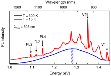
Typical PL spectra of the sample under study are presented in Fig. 1. A wide emission band with the maximum at around (), associated with the defects Sörman et al. (2000), is clearly observed at . The emission band transfers to a series of ZPLs when the sample is cooled down to . Two ZPLs at () and () correspond to the V1 and V2 defects, respectively Sörman et al. (2000); Fuchs et al. (2015). Several other ZPLs (labeled as PL2-PL4) are observed in the spectral range and related to the silicon-carbon defects Son et al. (2006).
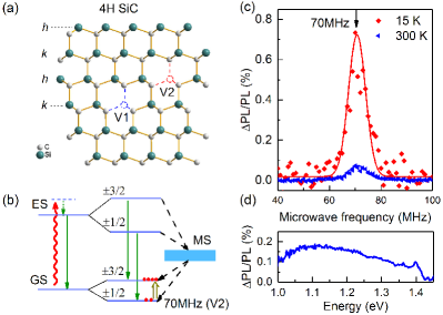
We concentrate on the V2 defect, associated with one of the two possible crystallographic sites in 4H-SiC (Fig. 2(a)). The mechanism of the zero-field ODMR associated with the defects is qualitatively explained in Fig. 2(b). The has spin in the ground state (GS) and excited state (ES) Kraus et al. (2014a). Optical excitation of the V2 defect into the ES is followed by two processes, radiative recombination to the ground state GS (solid lines) and non-radiative spin-dependent relaxation (dashed lines) through the metastable state (MS). Application of the resonant MW field at , which is equal to the zero-field splitting between the and states, changes the population of these spin sublevels. It breaks the equilibrium between the relaxation processes resulting in non-zero Kraus et al. (2014b).
Figure 2(c) presents the ODMR contrast () as a function of MW frequency. The PL is detected at at (shadow area in Fig. 1) and at the V2 ZPL at . To ensure that ODMR experiments are performed under optimum conditions, we investigate the laser power and MW power dependences at different temperatures. The ODMR contrast saturates in both cases Fischer et al. (2018) and we obtain and for and , respectively (Fig. 2(c)). Remarkably, the ODMR contrast only marginally depends on the detection energy over the PL band () at room temperature (Fig. 2(d)).
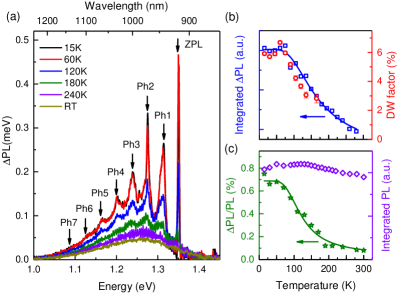
Next, we analyze how the change in the V2 emission induced by the MW depends on the detection wavelength. We set the MW frequency to (Fig. 2(c)) and the spectrum at is presented in Fig. 3(a). With decreasing temperature, the spectrum transfers to the ZPL and PSB consisting of seven equally-separated phonon replicas (Ph1 – Ph7). These spectra differ from the PL spectrum presented in Fig. 1, which is composed of overlapping contributions from different defects. Especially, the V1 and V2 PSBs are merged together, making their separation different. In the measurements, the MW frequency of is in the V2 spin resonance and, therefore, only the V2 PSB appears.
The spectrally integrated V2 as a function of temperature is presented in Fig. 3(b). The experimental data can be well reproduced using single activation energy Reshchikov et al. (2011)
| (1) |
We obtain from the best fit (solid line in Fig. 3(b)) the activation energy , which is equal within the experimental uncertainty to the local vibrational energy , as discussed hereafter. The unit-less coefficient is determined by the ratio of different relaxation rates Reshchikov et al. (2011). The is contributed by the spin polarization and the PL intensity. In order to separate these contributions, we plot in Fig. 3(c) detected at the ZPL and the spectrally integrated PL. The experimental data for can be also well fitted to Eq. (1) with the activation energy and replaced with . This indicates that the integrated PL intensity of the V2 is nearly temperature independent up to . Indeed, this is in agreement with the integrated PL of Fig. 3(c), where a small decrease with rising temperature can be attributed to the contribution of other defects with stronger temperature dependence.
Figure 3(a) clearly shows the PSB extends below (above ). Thus, the DW above 30% found in earlier experiments Banks et al. (2019) is definitely overestimated. Spectral integration of the experimental data in Fig. 3(a) results in the DW factor of about 6% for . This value should be corrected by the spectrally dependent readout contrast. Given spectral dependence of Fig. 2(d), the expected value for the DW factor falls between 6% and 9%. The DW decreases with temperature as shown in Fig. 3(b). As DW factor gives the fraction of elastic scattering, we might attribute the temperature reduction of its value to thermal motion effect Kittel (2004) and multiphonon contributions.
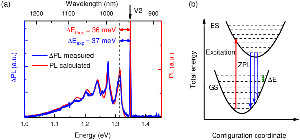
We determine the local vibrational energy as the separation between two adjacent phonon peaks in as presented in Fig. 4(a). The PSB formation is schematically presented in Fig. 4(b). The radiative recombination between the ES and GS is accompanied by phonon emission. The energy dispersion of these phonons differs from the bulk phonon dispersion because of the broken translation symmetry in the vicinity of the defect. In the next section, we present detailed theoretical analysis of the local vibrational modes.
Theory

We carried out DFT calculations as implemented in VASP Kresse and Hafner (1993) code to determine defect properties, configurational coordinate diagram, and vibrational modes which finally allow us to evaluate the PL lineshape. A plane wave basis with a cutoff energy of 450 eV is employed to represent the electronic wave functions. All structural relaxations and the vibrational properties were calculated using PBEsol Perdew et al. (2008) exchange-correlation functional. The geometry optimization continues until the energy differences and ionic forces are converged to less than eV and 0.01 eV/Å, respectively. The PL lineshape is calculated using the approach described in Ref. Alkauskas et al. (2014) and described in more detail below, which requires evaluation of the phonon spectra of the defective systems, but obtaining converged spectra requires large supercells that are computationally very demanding. Here, to speed up phonon calculations HIPHIVE Eriksson et al. (2019) package was used to extract interatomic force constants (IFCs). Second-order IFCs were constructed using the recursive feature elimination (RFE) optimizer by including pairs and triplets up to 4.2 and 3.6 Å, respectively. The modeled IFCs result in the validation root mean squared error of 13 meV/Å. The phonon frequencies and eigenvectors were finally assessed using PHONOPY software Togo and Tanaka (2015). To adjust the energy scales, i.e. the band gap and the position of the defect levels within, we additionally used HSE06 Krukau et al. (2006) to calculate total energies and Kohn-Sham levels. HSE functional has been shown to reproduce intradefect transition energies very well Deák et al. (2011). The calculated band gap of 3.25 eV is in excellent agreement to the experimental gap of 3.2 eV Lebedev (1999).
Theoretically, the determination of the average numbers of active phonons during the optical transition for mode with frequency is given by the unitless partial Huang-Rhys (HR) factor defined as MARKHAM (1959); Alkauskas et al. (2014)
| (2) |
where
| (3) |
Here, indicates the normalized displacement vector corresponding to mode and is mass of atom . and are the atomic coordinates in the ground and excited state. Thus, describes whether the vibrational mode is parallel to the change in the atomic coordinates. The fundamental spectral density of electron-phonon coupling can be determined as
| (4) |
where a broadening parameter is considered. It is worth mentioning that we assume the vibrational modes in the ground state and the excited state to be identical, and we use in Eq. 3 the evaluated in the ground state. Once is calculated, we make use of the method of generating function Miyakawa and Dexter (1970); Alkauskas et al. (2014) to derive the optical absorption spectrum
| (5) |
where the prefactor is the normalization constant and
| (6) |
is the generating function, where is defined by
| (7) |
We modelled the defect in a large 400-atoms supercell using 222 meshes for -point sampling. V2 defect corresponds to at the h-site, in the charge state, and with spin Kraus et al. (2014a). The HSE06-calculated Kohn-Sham levels are shown in Fig. 5(a), showing that the V2 defect introduces several electronic states deep in the band gap. The lowest energy electron configuration has the high spin state with three unpaired electrons (). We model the excitation by moving spin-down electron from the highest occupied to the first unoccupied electronic state, which is achieved by fixing the occupations of the relevant states in the DFT calculations. In the excited state, the two states related to the excitation become closer while others remain the same. From the DFT calculated total energies we can readily extract the configuration coordinate diagram, as shown in Fig. 5(b). We note that the potential energy curve is calculated using PBEsol, but the ZPL energy difference () is obtained using HSE06. The emission energy of 1.28 eV and the ZPL of 1.35 eV are in excellent agreement with the experimental values (the former corresponding to PSB maximum). Introduction of V2 defect also leads to expansion of the lattice by and .
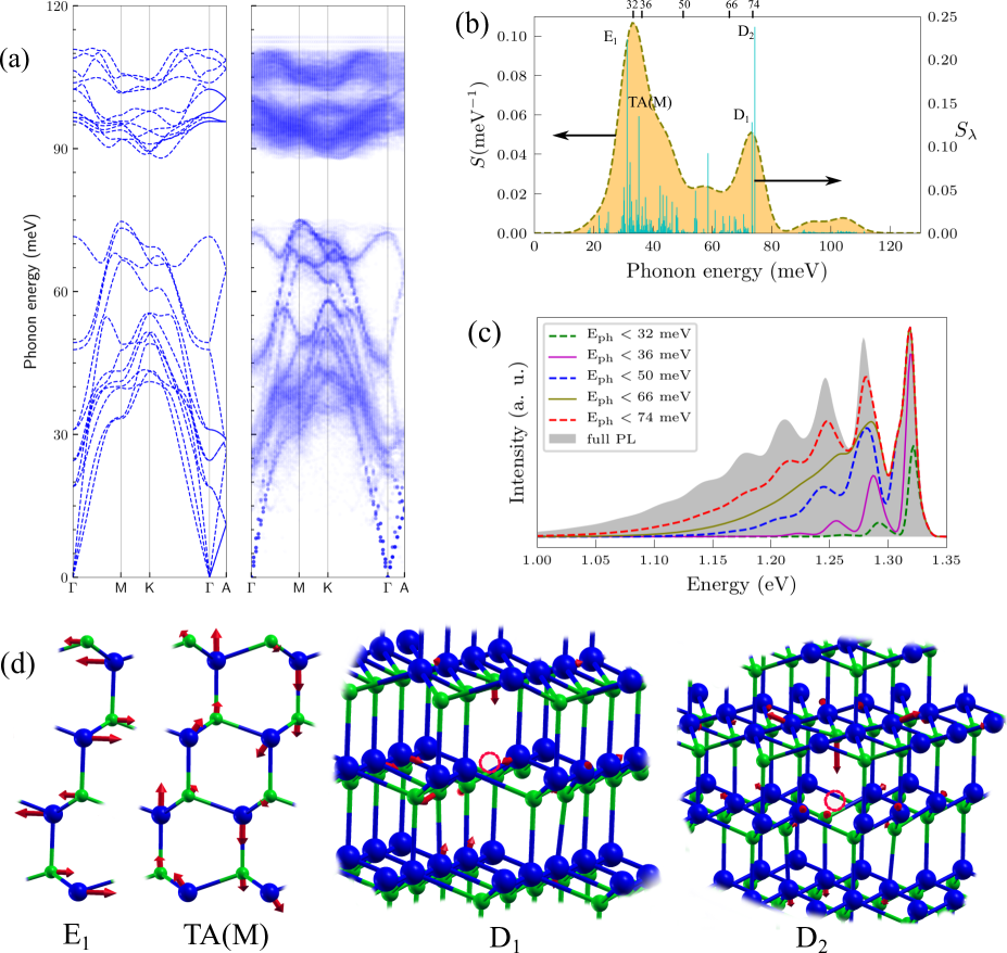
The defects can induce new vibrational modes, that are either resonant or anti-resonant with vibrational modes of the host crystal. To map the vibrational modes on the same Brillouin zone as for the pristine SiC, the unfolded phonon dispersion curve is illustrated in Fig. 6(a). We find that (i) the phonons between 20–40 meV and 90–110 meV are disturbed by the defects, but still follow the dispersion of the bands seen in the pristine system, and (ii) four localized vibrational modes (flat bands) appear at energies 73.45, 74.4, 111.47, and 112.8 meV. To find active phonons during emission process, the electron-phonon spectral function is calculated as shown in Fig. 6(b). Our calculation predicts that the PSB can be produced by a mix of about four phonon replicas: the double degenerate Raman-active E1 mode with energy 31.3 meV, the M-point transverse acoustic phonon active at 35.3 meV, and two defect modes appearing at energies 73.45 and 74.4 meV, denoted as D1 and D2, respectively. As illustrated in Fig 6(d), in D1 defect mode atoms up to second-nearest silicon neighbors from the vacancy center move, while for D2 case vibration is more intense and partially includes third nearest silicon atoms.
The partial HR factor () is the average number of phonon emitted during an optical transition. We predict the total HR factor , which corresponds to the average number of phonons emitted during an optical transition. As a result, the weight of ZPL (DW factor) defined by is 6.17, that is close to our measured value. As was illustrated in Fig. 4(a), our prediction for PL lineshape is in full agreement with the experiments. The PSB with seven peaks falls off at around 1.1 eV.
Following the analysis of vibrational modes, both bulk and defect phonons should contribute to the PSB. To get more insight into lineshape, we calculate partial PSB lineshape. To do this, we include phonons up to a specific energy in . The phonon energy (Eph) is chosen based on the values of partial HR factors. In this way, we can assess the contribution of different phonons into the total lineshape. As seen in Fig. 6(c), the first peak shape is completed by adding phonons up to 50 meV, but it quickly vanishes at lower energies. At this range of energy we have bulk phonons. The position of the first peak is at 36 meV lower than ZPL that is in agreement with the experiments. Clearly, the defect-induced phonons appeared around 74 meV are crucial in shaping optical emission spectrum at low temperature.
Discussion and Conclusions
Though the DW factor of 40% and 30% was reported for the V1 and V2 defects, respectively Nagy et al. (2018); Banks et al. (2019), the actual value is smaller due to the low detection efficiency at longer wavelength of the PSB. We experimentally estimated lower bound for the DW factor of 6%–9%. On the other hand, the calculations also yielded DW factor of about 6%, which suggests that the real value is indeed in this range. Though this value is at least by a factor of 2 larger than that of the NV defect in diamond Alkauskas et al. (2014), thus coupling to an optical resonator is necessary to realize quantum repeaters. The vibrational energy of 37 meV and 36 meV from experiments and calculations, respectively, were also in close agreement. This is an important parameter, which determines at which temperature the phonon-assisted spin-lattice relaxation mechanism associated with local vibrational modes is activated Simin et al. (2017).
To summarize, we have investigated the local vibrational structure of the V2 defect in a HPSI 4H-SiC wafer. The ODMR-based approach has enabled us to clearly separate the spectrally overlapped contribution from other intrinsic defects. We have found the resonant vibrational energy to be and estimated the lower bound for the DW factor to be 6%. We have applied DFT-based methodology to calculate and analyze the PL lineshape. Beside that, we have established that the contribution into the optical emission process is narrowed down to dominant bulk and defect-induced phonons. All together, the perfect agreement between the experimental data and theoretical calculations shows that our approach can be applied to a large number of highly-promising optically addressable spin qubits in all stable SiC polytypes, including vacancies Riedel et al. (2012), divacancies Falk et al. (2013) and transition metal color centers Zargaleh et al. (2016); Koehl et al. (2017). It is especially important when the spectral contribution from different defects is overlapped and cannot be separated otherwise. Exploring interaction of local vibrational modes with point defects, their spin, optical, mechanical and thermal properties can be predicted and understood, which is crucial by designing defect spins for quantum technologies. We believe that our results have not only considerable interest for experimental research of defect-related spin-vibrational properties but also becomes an important tool to study a large variety of defects in wide-bandgap semiconductors and 2D materials Gottscholl et al. (2019).
Acknowledgments
This work has been supported by the German Research Foundation (DFG) under Grants AS 310/5-1 and the Academy of Finland under Projects No. 286279 and 311058. We also thank CSC-IT Center Science Ltd. Finland and PRACE (HLRS, Stuttgart, Germany) for generous grants of computer time. The authors thank R. Narkowicz and K. Lenz for designing and characterization of the coplanar waveguides.
References
- Baranov et al. (2011) P. G. Baranov, A. P. Bundakova, A. A. Soltamova, S. B. Orlinskii, I. V. Borovykh, R. Zondervan, R. Verberk, and J. Schmidt, Silicon vacancy in SiC as a promising quantum system for single-defect and single-photon spectroscopy, Physical Review B 83, 125203 (2011).
- Koehl et al. (2011) W. F. Koehl, B. B. Buckley, F. J. Heremans, G. Calusine, and D. D. Awschalom, Room temperature coherent control of defect spin qubits in silicon carbide, Nature 479, 84 (2011).
- Riedel et al. (2012) D. Riedel, F. Fuchs, H. Kraus, S. Väth, A. Sperlich, V. Dyakonov, A. Soltamova, P. Baranov, V. Ilyin, and G. V. Astakhov, Resonant Addressing and Manipulation of Silicon Vacancy Qubits in Silicon Carbide, Physical Review Letters 109, 226402 (2012).
- Soltamov et al. (2012) V. A. Soltamov, A. A. Soltamova, P. G. Baranov, and I. I. Proskuryakov, Room Temperature Coherent Spin Alignment of Silicon Vacancies in 4H- and 6H-SiC, Physical Review Letters 108, 226402 (2012).
- Kraus et al. (2014a) H. Kraus, V. A. Soltamov, D. Riedel, S. Väth, F. Fuchs, A. Sperlich, P. G. Baranov, V. Dyakonov, and G. V. Astakhov, Room-temperature quantum microwave emitters based on spin defects in silicon carbide, Nature Physics 10, 157 (2014a).
- Castelletto et al. (2013) S. Castelletto, B. C. Johnson, V. Ivády, N. Stavrias, T. Umeda, A. Gali, and T. Ohshima, A silicon carbide room-temperature single-photon source, Nature Materials 13, 151 (2013).
- Christle et al. (2015) D. J. Christle, A. L. Falk, P. Andrich, P. V. Klimov, J. u. Hassan, N. T. Son, E. Janzén, T. Ohshima, and D. D. Awschalom, Isolated electron spins in silicon carbide with millisecond coherence times, Nature Materials 14, 160 (2015).
- Widmann et al. (2015) M. Widmann, S.-Y. Lee, T. Rendler, N. T. Son, H. Fedder, S. Paik, L.-P. Yang, N. Zhao, S. Yang, I. Booker, A. Denisenko, M. Jamali, S. A. Momenzadeh, I. Gerhardt, T. Ohshima, A. Gali, E. Janzén, and J. Wrachtrup, Coherent control of single spins in silicon carbide at room temperature, Nature Materials 14, 164 (2015).
- Fuchs et al. (2015) F. Fuchs, B. Stender, M. Trupke, D. Simin, J. Pflaum, V. Dyakonov, and G. V. Astakhov, Engineering near-infrared single-photon emitters with optically active spins in ultrapure silicon carbide, Nature Communications 6, 7578 (2015).
- Kraus et al. (2014b) H. Kraus, V. A. Soltamov, F. Fuchs, D. Simin, A. Sperlich, P. G. Baranov, G. V. Astakhov, and V. Dyakonov, Magnetic field and temperature sensing with atomic-scale spin defects in silicon carbide, Scientific Reports 4, 5303 (2014b).
- Simin et al. (2015) D. Simin, F. Fuchs, H. Kraus, A. Sperlich, P. G. Baranov, G. V. Astakhov, and V. Dyakonov, High-Precision Angle-Resolved Magnetometry with Uniaxial Quantum Centers in Silicon Carbide, Physical Review Applied 4, 014009 (2015).
- Simin et al. (2016) D. Simin, V. A. Soltamov, A. V. Poshakinskiy, A. N. Anisimov, R. A. Babunts, D. O. Tolmachev, E. N. Mokhov, M. Trupke, S. A. Tarasenko, A. Sperlich, P. G. Baranov, V. Dyakonov, and G. V. Astakhov, All-Optical dc Nanotesla Magnetometry Using Silicon Vacancy Fine Structure in Isotopically Purified Silicon Carbide, Physical Review X 6, 031014 (2016).
- Niethammer et al. (2016) M. Niethammer, M. Widmann, S.-Y. Lee, P. Stenberg, O. Kordina, T. Ohshima, N. T. Son, E. Janzén, and J. Wrachtrup, Vector Magnetometry Using Silicon Vacancies in 4H-SiC Under Ambient Conditions, Physical Review Applied 6, 034001 (2016).
- Cochrane et al. (2016) C. J. Cochrane, J. Blacksberg, M. A. Anders, and P. M. Lenahan, Vectorized magnetometer for space applications using electrical readout of atomic scale defects in silicon carbide, Scientific Reports 6, 37077 (2016).
- Soykal and Reinecke (2017) Ö. O. Soykal and T. L. Reinecke, Quantum metrology with a single spin-3/2 defect in silicon carbide, Physical Review B 95, 081405 (2017).
- Soltamov et al. (2019) V. A. Soltamov, C. Kasper, A. V. Poshakinskiy, A. N. Anisimov, E. N. Mokhov, A. Sperlich, S. A. Tarasenko, P. G. Baranov, G. V. Astakhov, and V. Dyakonov, Excitation and coherent control of spin qudit modes in silicon carbide at room temperature, Nature Communications 10, 1678 (2019).
- Wolfowicz et al. (2019) G. Wolfowicz, C. P. Anderson, S. J. Whiteley, and D. D. Awschalom, Heterodyne detection of radio-frequency electric fields using point defects in silicon carbide, Applied Physics Letters 115, 043105 (2019).
- Anisimov et al. (2016) A. N. Anisimov, D. Simin, V. A. Soltamov, S. P. Lebedev, P. G. Baranov, G. V. Astakhov, and V. Dyakonov, Optical thermometry based on level anticrossing in silicon carbide, Scientific Reports 6, 33301 (2016).
- Zhou et al. (2017) Y. Zhou, J. Wang, X. Zhang, K. Li, J. Cai, and W. Gao, Self-Protected Thermometry with Infrared Photons and Defect Spins in Silicon Carbide, Physical Review Applied 8, 044015 (2017).
- Yang et al. (2014) L.-P. Yang, C. Burk, M. Widmann, S.-Y. Lee, J. Wrachtrup, and N. Zhao, Electron spin decoherence in silicon carbide nuclear spin bath, Physical Review B 90, 241203 (2014).
- Carter et al. (2015) S. G. Carter, Ö. O. Soykal, P. Dev, S. E. Economou, and E. R. Glaser, Spin coherence and echo modulation of the silicon vacancy in 4H-SiC at room temperature, Physical Review B 92, 161202 (2015).
- Seo et al. (2016) H. Seo, A. L. Falk, P. V. Klimov, K. C. Miao, G. Galli, and D. D. Awschalom, Quantum decoherence dynamics of divacancy spins in silicon carbide, Nature Communications 7, 12935 (2016).
- Embley et al. (2017) J. S. Embley, J. S. Colton, K. G. Miller, M. A. Morris, M. Meehan, S. L. Crossen, B. D. Weaver, E. R. Glaser, and S. G. Carter, Electron spin coherence of silicon vacancies in proton-irradiated 4H-SiC, Physical Review B 95, 045206 (2017).
- Simin et al. (2017) D. Simin, H. Kraus, A. Sperlich, T. Ohshima, G. V. Astakhov, and V. Dyakonov, Locking of electron spin coherence above 20 ms in natural silicon carbide, Physical Review B 95, 161201(R) (2017).
- Fischer et al. (2018) M. Fischer, A. Sperlich, H. Kraus, T. Ohshima, G. V. Astakhov, and V. Dyakonov, Highly Efficient Optical Pumping of Spin Defects in Silicon Carbide for Stimulated Microwave Emission, Physical Review Applied 9, 2126 (2018).
- Economou and Dev (2016) S. E. Economou and P. Dev, Spin-photon entanglement interfaces in silicon carbide defect centers, Nanotechnology 27, 504001 (2016).
- Christle et al. (2017) D. J. Christle, P. V. Klimov, C. F. de las Casas, K. Szász, V. Ivády, V. Jokubavicius, J. Ul Hassan, M. Syväjärvi, W. F. Koehl, T. Ohshima, N. T. Son, E. Janzén, A. Gali, and D. D. Awschalom, Isolated Spin Qubits in SiC with a High-Fidelity Infrared Spin-to-Photon Interface, Physical Review X 7, 021046 (2017).
- Nagy et al. (2019) R. Nagy, M. Niethammer, M. Widmann, Y.-C. Chen, P. Udvarhelyi, C. Bonato, J. u. Hassan, R. Karhu, I. G. Ivanov, N. T. Son, J. R. Maze, T. Ohshima, Ö. O. Soykal, A. Gali, S.-Y. Lee, F. Kaiser, and J. Wrachtrup, High-fidelity spin and optical control of single silicon-vacancy centres in silicon carbide, Nature Communications 10, 1954 (2019).
- Udvarhelyi et al. (2019) P. Udvarhelyi, R. Nagy, F. Kaiser, S.-Y. Lee, J. Wrachtrup, and A. Gali, Spectrally Stable Defect Qubits with no Inversion Symmetry for Robust Spin-To-Photon Interface, Physical Review Applied 11, 044022 (2019).
- Kraus et al. (2017) H. Kraus, D. Simin, C. Kasper, Y. Suda, S. Kawabata, W. Kada, T. Honda, Y. Hijikata, T. Ohshima, V. Dyakonov, and G. V. Astakhov, Three-Dimensional Proton Beam Writing of Optically Active Coherent Vacancy Spins in Silicon Carbide, Nano Letters 17, 2865 (2017).
- Wang et al. (2017) J. Wang, X. Zhang, Y. Zhou, K. Li, Z. Wang, P. Peddibhotla, F. Liu, S. Bauerdick, A. Rudzinski, Z. Liu, and W. Gao, Scalable Fabrication of Single Silicon Vacancy Defect Arrays in Silicon Carbide Using Focused Ion Beam, ACS Photonics 4, 1054 (2017).
- Wang et al. (2019) J.-F. Wang, Q. Li, F.-F. Yan, H. Liu, G.-P. Guo, W.-P. Zhang, X. Zhou, L.-P. Guo, Z.-H. Lin, J.-M. Cui, X.-Y. Xu, J.-S. Xu, C.-F. Li, and G.-C. Guo, On-Demand Generation of Single Silicon Vacancy Defects in Silicon Carbide, ACS Photonics 6, 1736 (2019).
- Fuchs et al. (2013) F. Fuchs, V. A. Soltamov, S. Väth, P. G. Baranov, E. N. Mokhov, G. V. Astakhov, and V. Dyakonov, Silicon carbide light-emitting diode as a prospective room temperature source for single photons, Scientific Reports 3, 1637 (2013).
- Lohrmann et al. (2015) A. Lohrmann, N. Iwamoto, Z. Bodrog, S. Castelletto, T. Ohshima, T. J. Karle, A. Gali, S. Prawer, J. C. McCallum, and B. C. Johnson, Single-photon emitting diode in silicon carbide, Nature Communications 6, 7783 (2015).
- Sato et al. (2018) S.-i. Sato, T. Honda, T. Makino, Y. Hijikata, S.-Y. Lee, and T. Ohshima, Room Temperature Electrical Control of Single Photon Sources at 4H-SiC Surface, ACS Photonics , acsphotonics.8b00375 (2018).
- Widmann et al. (2018) M. Widmann, M. Niethammer, T. Makino, T. Rendler, S. Lasse, T. Ohshima, J. Ul Hassan, N. Tien Son, S.-Y. Lee, and J. Wrachtrup, Bright single photon sources in lateral silicon carbide light emitting diodes, Applied Physics Letters 112, 231103 (2018).
- Klimov et al. (2014) P. V. Klimov, A. L. Falk, B. B. Buckley, and D. D. Awschalom, Electrically Driven Spin Resonance in Silicon Carbide Color Centers, Physical Review Letters 112, 087601 (2014).
- Falk et al. (2014) A. L. Falk, P. V. Klimov, B. B. Buckley, V. Ivády, I. A. Abrikosov, G. Calusine, W. F. Koehl, A. Gali, and D. D. Awschalom, Electrically and Mechanically Tunable Electron Spins in Silicon Carbide Color Centers, Physical Review Letters 112, 187601 (2014).
- Widmann et al. (2019) M. Widmann, M. Niethammer, D. Y. Fedyanin, I. A. Khramtsov, T. Rendler, I. D. Booker, J. Ul Hassan, N. Morioka, Y.-C. Chen, I. G. Ivanov, N. T. Son, T. Ohshima, M. Bockstedte, A. Gali, C. Bonato, S.-Y. Lee, and J. Wrachtrup, Electrical Charge State Manipulation of Single Silicon Vacancies in a Silicon Carbide Quantum Optoelectronic Device, Nano Letters 19, 7173 (2019).
- Whiteley et al. (2019) S. J. Whiteley, G. Wolfowicz, C. P. Anderson, A. Bourassa, H. Ma, M. Ye, G. Koolstra, K. J. Satzinger, M. V. Holt, F. J. Heremans, A. N. Cleland, D. I. Schuster, G. Galli, and D. D. Awschalom, Spin–phonon interactions in silicon carbide addressed by Gaussian acoustics, Nature Physics 15, 490 (2019).
- Poshakinskiy and Astakhov (2019) A. V. Poshakinskiy and G. V. Astakhov, Optically detected spin-mechanical resonance in silicon carbide membranes, Physical Review B 100, 094104 (2019).
- Castelletto et al. (2014) S. Castelletto, B. C. Johnson, C. Zachreson, D. Beke, I. Balogh, T. Ohshima, I. Aharonovich, and A. Gali, Room Temperature Quantum Emission from Cubic Silicon Carbide Nanoparticles, ACS Nano 8, 7938 (2014).
- Muzha et al. (2014) A. Muzha, F. Fuchs, N. V. Tarakina, D. Simin, M. Trupke, V. A. Soltamov, E. N. Mokhov, P. G. Baranov, V. Dyakonov, A. Krueger, and G. V. Astakhov, Room-temperature near-infrared silicon carbide nanocrystalline emitters based on optically aligned spin defects, Applied Physics Letters 105, 243112 (2014).
- Sörman et al. (2000) E. Sörman, N. Son, W. Chen, O. Kordina, C. Hallin, and E. Janzén, Silicon vacancy related defect in 4H and 6H SiC, Physical Review B 61, 2613 (2000).
- Son et al. (2006) N. Son, P. Carlsson, J. ul Hassan, E. Janzén, T. Umeda, J. Isoya, A. Gali, M. Bockstedte, N. Morishita, T. Ohshima, and H. Itoh, Divacancy in 4H-SiC, Physical Review Letters 96, 055501 (2006).
- Gali et al. (2011) A. Gali, T. Simon, and J. E. Lowther, An ab initio study of local vibration modes of the nitrogen-vacancy center in diamond, New Journal of Physics 13, 025016 (2011).
- Alkauskas et al. (2014) A. Alkauskas, B. B. Buckley, D. D. Awschalom, and C. G. Van de Walle, First-principles theory of the luminescence lineshape for the triplet transition in diamond NV centres, New Journal of Physics 16, 073026 (2014).
- Nagy et al. (2018) R. Nagy, M. Widmann, M. Niethammer, D. B. R. Dasari, I. Gerhardt, Ö. O. Soykal, M. Radulaski, T. Ohshima, J. Vučković, N. T. Son, I. G. Ivanov, S. E. Economou, C. Bonato, S.-Y. Lee, and J. Wrachtrup, Quantum Properties of Dichroic Silicon Vacancies in Silicon Carbide, Physical Review Applied 9, 034022 (2018).
- Banks et al. (2019) H. B. Banks, Ö. O. Soykal, R. L. Myers-Ward, D. K. Gaskill, T. L. Reinecke, and S. G. Carter, Resonant Optical Spin Initialization and Readout of Single Silicon Vacancies in 4H-SiC, Physical Review Applied 11, 024013 (2019).
- Ivády et al. (2018) V. Ivády, I. A. Abrikosov, and A. Gali, First principles calculation of spin-related quantities for point defect qubit research, npj Computational Materials 4, 45 (2018).
- Bockstedte et al. (2018) M. Bockstedte, F. Schütz, T. Garratt, V. Ivády, and A. Gali, Ab initio description of highly correlated states in defects for realizing quantum bits, npj Quantum Materials 3, 5645 (2018).
- Reshchikov et al. (2011) M. A. Reshchikov, A. A. Kvasov, M. F. Bishop, T. McMullen, A. Usikov, V. Soukhoveev, and V. A. Dmitriev, Tunable and abrupt thermal quenching of photoluminescence in high-resistivity Zn-doped GaN, Physical Review B 84, 075212 (2011).
- Kittel (2004) C. Kittel, Introduction to Solid State Physics, 8th ed. (Wiley, 2004).
- Kresse and Hafner (1993) G. Kresse and J. Hafner, Ab Initio Molecular Dynamics For Liquid Metals Phys. Rev. B 47, 558 (1993).
- Perdew et al. (2008) J. P. Perdew, A. Ruzsinszky, G. I. Csonka, O. A. Vydrov, G. E. Scuseria, L. A. Constantin, X. Zhou, and K. Burke, Restoring the Density-Gradient Expansion for Exchange in Solids and Surfaces Phys. Rev. Lett. 100, 136406 (2008).
- Eriksson et al. (2019) F. Eriksson, E. Fransson, and P. Erhart, The hiphive package for the extraction of high-order force constants by machine learning Advanced Theory and Simulations 2, 1800184 (2019) .
- Togo and Tanaka (2015) A. Togo and I. Tanaka, First Principles Phonon Calculations In Materials Science, Scr. Mater. 108, 1 (2015).
- Krukau et al. (2006) A. V. Krukau, O. A. Vydrov, A. F. Izmaylov, and G. E. Scuseria, Influence of the exchange screening parameter on the performance of screened hybrid functionals The Journal of Chemical Physics 125, 224106 (2006).
- Deák et al. (2011) P. Deák, B. Aradi, and T. Frauenheim, Polaronic effects in TiO2 calculated by the HSE06 hybrid functional: Dopant passivation by carrier self-trapping Phys. Rev. B 83, 155207 (2011).
- Lebedev (1999) A. A. Lebedev, Deep level centers in silicon carbide: A review Semiconductors 33, 107 (1999).
- MARKHAM (1959) J. J. Markham, Interaction of normal modes with electron traps Rev. Mod. Phys. 31, 956 (1959).
- Miyakawa and Dexter (1970) T. Miyakawa and D. L. Dexter, Phonon sidebands, multiphonon relaxation of excited states, and phonon-assisted energy transfer between ions in solids Phys. Rev. B 1, 2961 (1970).
- Falk et al. (2013) A. L. Falk, B. B. Buckley, G. Calusine, W. F. Koehl, V. V. Dobrovitski, A. Politi, C. A. Zorman, P. X. L. Feng, and D. D. Awschalom, Polytype control of spin qubits in silicon carbide, Nature Communications 4, 1819 (2013).
- Zargaleh et al. (2016) S. A. Zargaleh, B. Eble, S. Hameau, J. L. Cantin, L. Legrand, M. Bernard, F. Margaillan, J. S. Lauret, J. F. Roch, H. J. von Bardeleben, E. Rauls, U. Gerstmann, and F. Treussart, Evidence for near-infrared photoluminescence of nitrogen vacancy centers in 4H-SiC, Physical Review B 94, 86 (2016).
- Koehl et al. (2017) W. F. Koehl, B. Diler, S. J. Whiteley, A. Bourassa, N. T. Son, E. Janzén, and D. D. Awschalom, Resonant optical spectroscopy and coherent control of Cr4+ spin ensembles in SiC and GaN, Physical Review B 95, 035207 (2017).
- Gottscholl et al. (2019) A. Gottscholl, M. Kianinia, V. Soltamov, C. Bradac, C. Kasper, K. Krambrock, A. Sperlich, M. Toth, I. Aharonovich, and V. Dyakonov, Room Temperature Initialisation and Readout of Intrinsic Spin Defects in a Van der Waals Crystal, arXiv:1906.03774 .