Scanned single-electron probe inside a silicon electronic device
Abstract
Solid-state devices can be fabricated at the atomic scale, with applications ranging from classical logic to current standards and quantum technologies. While it is very desirable to probe these devices and the quantum states they host at the atomic scale, typical methods rely on long-ranged capacitive interactions, making this difficult. Here we probe a silicon electronic device at the atomic scale using a localized electronic quantum dot induced directly within the device at a desired location, using the biased tip of a low-temperature scanning tunneling microscope. We demonstrate control over short-ranged tunnel coupling interactions of the quantum dot with the device’s source reservoir using sub-nm position control of the tip, and the quantum dot energy level using a voltage applied to the device’s gate reservoir. Despite the nm proximity of the quantum dot to the metallic tip, we find the gate provides sufficient capacitance to enable a high degree of electric control. Combined with atomic scale imaging, we use the quantum dot to probe applied electric fields and charge in individual defects in the device. This capability is expected to aid in the understanding of atomic-scale devices and the quantum states realized in them.
The miniaturization of solid-state devices has driven tremendous improvements in their performance and functionality. For example, the information revolution has been enabled through decades of continuous miniaturization of silicon complementary metal-oxide-semiconductor devices. Device miniaturization also permits the localization and control of single electrons in solids, which has led to new fundamental physics experiments(Goldhaber1998, ), new current standards (Pekola2013, ; Rossi2014, ) and could enable the realization of quantum computers (Loss1998, ; Kane1998, ; Petta2005, ; Koppens2006, ) and quantum simulators(Feynman1982, ; Singha2011, ; Salfi2016, ; Hensgens2017, ). Such single electron devices can employ quantum dots (QD) (Kouwenhoven2001, ; Hanson2007, ; Zwanenburg2013, ) or active atoms placed with atomic-scale precision in solids using scanning tunnelling microscopy (STM)(Fuechsle2012, ; Zwanenburg2013, ; Folsch2014, ; Huff2018, ; He2019, ).
With ever-shrinking device sizes, real-space techniques for probing their properties and the complex states they host are becoming increasingly important. One notable technique, the scanning single electron transistor(Yoo1997, ) (SSET) monitors the capacitive response of an electron localized on scanning single-electron transistor to probe electrons in a device. Another notable technique, scanning gate microscopy (SGM)(Sellier2011, ) records the electrostatic response of the device’s conductance to a scanned conductive tip. The interaction mechanism at play in the SSET and SGM is capacitive (electrostatic), which inherently limits functionality and spatial resolution.
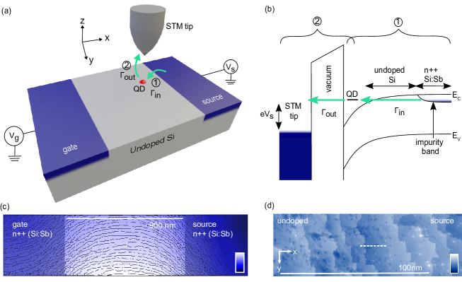
Here we go beyond the electrostatic interaction paradigm of SSET and SGM by showing that a spatially localized single-electron QD probe can be induced at an arbitrary location inside an electronic device, and made to interact not only capacitively, but also through tunneling interactions with electrons in the device. The method relies on electrostatically inducing a QD at a desired location with sub-nm precision using a biased atomically sharp tip of a low temperature scanning tunnelling microscope (LT-STM) operating at 4.2 Kelvin(Dombrowski1999, ; Freitag2016, ; Salfi2018, ). Our device consists of donor implanted source and gate reservoirs and the QD probe is induced within the device, beneath a hydrogen terminated silicon surface. This surface is atomically flat, similar to surfaces found in other materials relevant for electronic devices including two-dimensional materials(Dombrowski1999, ; Freitag2016, ).
Working in the regime of single-electron tunnelling through the induced QD, we demonstrate the ability to tune the tunnel coupling of the QD to the dopant-atom source reservoir by moving the STM tip, and use this to characterize the decay length of our probe QD wavefunction, which we find to be nm. This technique works alongside the traditional use of STM to image device surfaces with atomic resolution. Our study is performed on a multi-terminal device, having both source and gate electrodes (Figure 1a), which differs significantly from previous studies(Dombrowski1999, ; Freitag2016, ; Shim2019, ; Wagner2019, ). We find that the QD state energy can be controlled using the device’s gate voltage. The gate lever arm, which expresses the ratio of the capacitive coupling between the QD and the gate, to the total capacitance, is found to be , offering a high degree of electric control. Surprisingly, the QD capacitance is dominated by the capacitive coupling to the source terminal in the device, despite the nm proximity of the QD state to the metallic tip that induces it.
The QD state energy also reacts to atomic scale defects that we directly observe with atomic resolution, allowing us to map the defect charge state directly using the QD. Extended to devices based on arrays of dopant atoms placed with atomic precision, we envision these new experimental capabilities could be used to characterize or enhance the functionality of atomic scale devices. For example, the induced QD could be used to induce a highly tunable super-exchange(Malinowski2019, ) between donor atoms(Srinivasa2015, ), or to implement local spin readout(Elzerman2004, ) on atomic structures consisting of interacting dopant atoms forming quantum simulators(Salfi2016, ).
Before discussing our experiment, we first describe the concept of our induced QD probe. When a negative sample bias is applied to a semiconductor with respect to an STM tip, an electric field is induced by the tip that locally bends the semiconductor bands downward to create an attractive potential for electrons. We use this capability to trap individual electrons beneath our atomically flat surface(Salfi2018, ). This is done in the insulating p-type region of a device, fabricated as a planar n++/p/n++ junction over a p-type substrate (see supp. mat.), where the antimony doped n++ regions form electron reservoirs that act as a source and gate (Figure 1a,c). Since the electric field is strongest below the tip, the QD follows the position of the tip, and in our experiment, we move the QD toward the source reservoir, performing resonant single-electron tunnelling spectroscopy on the QD. Resonant tunnelling (Figure 1b) is detected as a measured step (peak) in current (conductance) when the QD state is on resonance with the source reservoir. We control the electron tunnel-in rate from the source reservoir to the QD using the sub-nanometre positioning precision of the STM tip along and (Figure 1a) and track the variation of through the measured single-electron tunnelling current , where is the tunnel rate from the QD out to the tip(Bonet2002, ) and is the electronic charge. To observe the variation of , we work in the regime where , which can be achieved by varying using the tip-sample separation (vacuum barrier width). A voltage is applied to the gate reservoir located approximately nm away from the source reservoir, which we use to tune the energy of the QD. As expected for a single-electron device, this changes the corresponding bias at which a QD state is on resonance with the source reservoir.
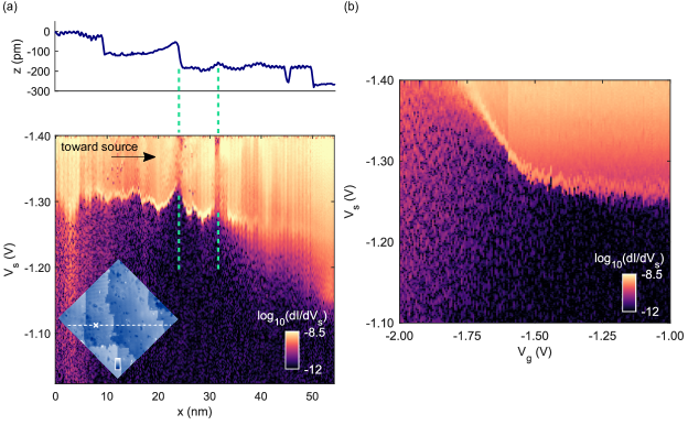
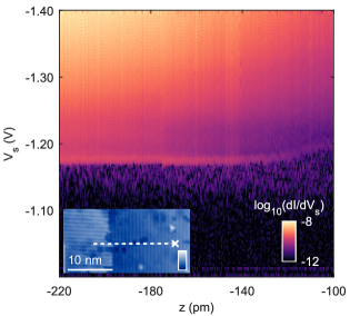
Following fabrication of the device (Figure 1a and supp. mat.), we first imaged the device at the level of its global topographical features, and then in detail at the junction between the undoped region and the source region (Figure 1c,d). The device is identified by the bunching of step edges at both the gate/undoped and undoped/source junctions (Figure 1c). The distinct difference in appearance of dangling bonds in the doped and undoped regions confirms that the step-edge bunching occurs at the junction (Figure 1d). Dangling bonds appear ‘bright’ (negatively charged) in doped regions and ‘dark’ (positively charged) in undoped regions in filled state imaging(Labidi2015, ). Spatially resolved spectroscopy was performed at several lines traversing the junction, such as the one in Figure 1d.
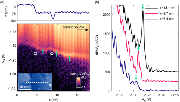
The differential conductance , obtained by numerically differentiating the current , is shown as a function of source-tip bias and tip position in Figure 2a for the line shown in the STM inset. The corresponding topography recorded by the tip is plotted above the conductance map. From – nm, no clear resonance is seen as tunnelling to any localized state below the tip is prevented by the wide substrate tunnel barrier. As the tip moves closer to the source reservoir, the resonance peak becomes apparent for nm at a voltage V, and remains visible for increasing . We also note a weak background corresponding to direct tunnelling from the occupied valence band to the tip energy starting around V to V, as expected near an n-type lead (Salfi2014, ). Importantly, only the feature emerging at V has a resonant peak lineshape indicative of a QD state. We plot in Figure 2b the numerically differentiated conductance for traces of Figure 2a at the coordinates nm, nm and nm.
The combination of the resonance lineshape, its continuous spatial nature, and its increasing amplitude with decreasing distance from the reservoir allows us to confidently rule out that the resonance is due to tunnelling through stray dopants at the junction or surface dangling bonds(Salfi2014, ; Taucer2014, ; Labidi2015, ). The possibility that the peak emerging at nm consists of a QD state hybridized with dopants or dangling bonds can also be ruled out, because we do not observe the spectroscopic signature of dopants(Salfi2014, ) and dangling bonds(Taucer2014, ) in Figure 2a. For nm however, we note the conductance of the resonance levels off and even slightly decreases. It is difficult to isolate the reason for this decrease but we note that it coincides with the QD reaching localized states(Salfi2014, ) observed in our measured spectra (supp. mat. Figure 6). Indeed, fixed localized states in the sample are expected to be found when the tip enters the reservoir region for nm, since the reservoir is composed of antimony donor levels that are energetically below the induced QD resonance. Tunnelling here is expected to be more complex because of the potential hybridization of the induced QD with donors(Salfi2018, ) which have a high concentration in the reservoir.
The QD energy and tunnelling rate to the QD are expected to be influenced when the QD encounters and interacts with surface defects. This is seen in Figure 2a as two disturbances of the resonance energy in , indicated by the square and star that occur at positions where a step-edge and atomic defect are found on the surface, respectively. In measurements performed along a different line towards the reservoir (supp. mat. Figure 5), we observe strong disturbances of the tunnelling current as the QD encounters accumulated negative charge at a step edge, and from a negatively charged (2e-) dangling bond, at = nm and nm respectively. For both disturbances, the bias required to maintain resonant tunnelling through the QD decreases (more negative) as it moves toward the negative charge, before subsequently increasing as it moves away. This is expected, because the induced QD energy level is sensitive to surface charge in the device through the Coulomb interaction.
We now investigate the interaction of the induced QD with the planar electric field established between the biased source and gate reservoirs. In Figure 2a, the voltage required to bring the QD on resonance with the source reservoir increases from V to V over a nm distance between = – nm as the QD approaches the reservoir. This is expected because of the oriented electric field that exists between the source and the fixed gate V during spectroscopy, which introduces an -dependent offset to the QD energy. Assuming a resonance around V, a gate voltage V, and a source to gate distance of approximately nm, we estimate MV/m, varying slightly for V to V where the resonance is found. Since the gate voltage is always more negative compared to during measurements, the electric potential is more repulsive when the QD is closer to the gate reservoir. As a result, when the QD moves away from the gate i.e. tip position increases, less tip-induced band bending and a higher is required to bring the QD state on resonance with the source reservoir. From , we quantify the ability of the sample-tip bias voltage to change the energy of the QD state with the lever arm parameter , where and , are differing values of source-tip bias. By equating the energetic change of the resonance in Figure 2a toward lower values as increases, to the expected energy level change due to , we obtain a value of . This is in good agreement with values of independently obtained by fitting to a model of single electron tunnelling between Fermi reservoirs through a quantized state (Foxman1993, ), and in agreement with previously extracted values of the lever arm for a tip-induced QD(Salfi2018, ). Using this model, where fitting is facilitated by increased smoothing of the measured current, we find varying from to for increasing between – nm, as the induced QD approaches the reservoir. For the two different intervals in which only have approximately nm overlap, the estimated values for match closely, giving us confidence in the obtained values. We note that varying and could also change the QD potential and its energy spectrum(Dombrowski1999, ), however, the behaviour of the ground state seems to follow a relatively simple model with an energy shift of the level due to the oriented electric field.
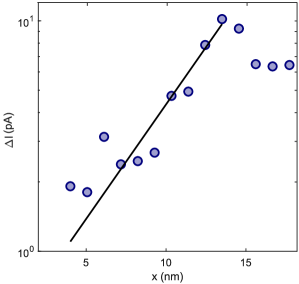
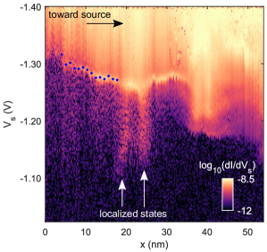
We estimate the decay of the tail of the induced QD wavefunction in space using the measured change in induced current through the QD as it is moved toward the source reservoir with increasing . We plot in Figure 3 using the measured current of Figure 6 (supp. mat.) before the QD encounters the localized states. The blue dots plotted on the resonance of the conductance map indicate the position of the traces in and the peaks in used. For traces along the resonance, we find exponentially increasing between = – nm before slightly decreasing nm prior to encountering the localized states. This observation suggests that the appearance of the resonance at nm is due to the increasing tunnel coupling as the QD moves towards the source reservoir. Indeed, we work at a tip-sample separation that establishes a tunnel rate where is larger than the tunnel rate from source reservoir to the QD , which depends on the QD-reservoir distance. This regime can be achieved by starting sufficiently far away from the reservoir such that is much smaller than our measurement resolution of around fA. Notably, we verified this regime of operation by tip-height dependent measurements closer to the reservoir (supp. mat. Figure 7).
Between = – nm where we measure resonant tunnelling only between the reservoir and the QD, we obtain a best fit value for of = nm-1 (Figure 3, black line). To relate this to the decay of the induced QD wavefunction in space, we compare the decay to a model for the tunnel coupling from the source reservoir to the QD that approximates the tail of the QD wavefunction as , where is the decay length. With an abrupt model for the reservoir electrons (supp. mat.), we obtain , where is the position of the reservoir relative to the QD, and from this nm using the extracted . We note that our assumption of an abrupt reservoir makes this an upper bound on the actual decay. Notably, the slowly varying tail is convenient to controllably tunnel couple the QD to elements such as individual donors in devices. For example, highly tunable tunnel coupling would be advantageous for local spin readout on small scale dopant-based quantum simulators(Salfi2016, ; Le2017, ; Le2019, ) where STM tips can be positioned with sub-nanometre accuracy.
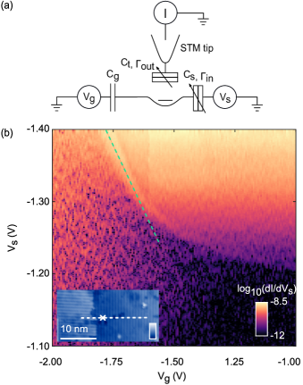
By sweeping the gate voltage applied to the gate donor reservoir, we demonstrate the ability to electrically tune the energy of the QD at a fixed tip-sample voltage using the gate. Figure 4a shows a schematic of our device: capacitive interactions between the QD and the tip, source and gate reservoirs are represented by , and respectively, and are present as we keep the tip fixed in space whilst varying . We vary the gate voltage over a V range from V to V to examine the gating characteristics of the QD, with the tip held at the position indicated by the marker on the line in the STM inset of Figure 4b. Figure 4b shows the conductance through the QD as a function of and . The green line indicates linear behaviour of the gate during resonance for V. When is increased toward V, higher values of are required to keep the QD state on resonance with the source reservoir. As expected, a more positive gate with an increasingly attractive potential pulls the level of the QD lower in energy. Thus, increases and the amount of tip-induced band bending required is lessened, with a corresponding decrease in current through the QD as a consequence of the widening tunnel barrier.
We analyze the capacitive coupling of the quantum dot, and extract the gate lever arm in the voltage range to V where the gate acts linearly. Here, the change in bias voltage required to maintain resonant tunnelling is given by , where is the sum of all capacitances between the QD and its environment, including a stray capacitance not shown in Figure. 4a. In this regime, is extracted from the gradient of the green line. Using the lever arm extracted from the source bias dependent measurement, where (supp. mat.), we find that and obtain a gate lever arm for the induced quantum dot of . Evidently, the QD capacitive coupling is dominated by , with an appreciable gate capacitive coupling, where (supp. mat.) despite the metal tip being only nm away from the QD. The effect of the gate weakens for values V and higher and flattens out around V. This behaviour could be due to an enhancement of stray capacitance due to an accumulation of charges in or near the source, by the gate. The control of the induced QD by the gate is important for the potential use of the QD to understand the operation of devices or to probe quantum states induced in devices.
In conclusion, we have demonstrated the ability to induce a single localized electron QD within a device, and to tune its tunnel coupling to a source electrode and electric interaction with a gate electrode within a silicon electronic device. We find that the single electron QD reacts to charges present in the device, both due to individual defects, and due to voltages applied to gates in the device. With the sub-nanometre precision of the tip and the slowly-varying nature of the ground state QD wavefunction, a high level of tunnel coupling control to donor-based electrodes is possible. This opens up the possibility to use tip-induced quantum dots to characterize devices and the quantum states they host, and even to add new device functionality. We expect this technique will be applicable to advanced devices based on materials that can be engineered at the atomic scale, because it is compatible with LT-STM, the most common technique for probing atomic-scale materials and assembling atomic-scale devices(Folsch2014, ; Huff2018, ).
Acknowledgements
K.S.H.N. would like to acknowledge S. Loth for useful discussions. We acknowledge support from the ARC Centre of Excellence for Quantum Computation and Communication Technology (CE170100012) and an ARC Discovery Project (DP180102620). J.S. acknowledges financial support from an ARC DECRA fellowship (DE1601101490) and from the National Science and Engineering Research Council. B.C.J. and J.C.MC acknowledge the AFAiiR node of the NCRIS Heavy Ion Capability for access to ion-implantation facilities.
Author Contributions
J.S. proposed the idea to probe an electronic device using an induced quantum dot, with input from B.V. and S.R. S.R. proposed the in-situ devices scheme with input from B.V. and J.S. K.S.H.N. performed all the measurements and analysis with input from J.S., B.V. and S.R. B.V., B.C.J. and J.C.MC. led the design, fabrication, vacuum preparation and measurement scheme for in-situ use of the device with input from J.S. and S.R. K.S.H.N. wrote the manuscript with guidance from J.S. and input from B.V. and S.R.
Supplementary Information
.1 Device Fabrication
All measurements are performed using an Omicron LT STM at K. A commercial p-type boron doped silicon wafer is used with a doping density of cm-3, corresponding to a resistivity of 1–10 cm. Antimony ion beam implantation is performed such that a dopant layer is created just below the silicon surface with a density of 11015 cm-2 at selected regions of the sample with the use of a nm thick HSQ oxide mask. Once cleaned, the sample is degassed at C for 12 hours. Following this, two additional flashes at C are performed, each for 10 seconds. The temperature is then rapidly brought to C before slowly decreasing the temperature at a rate of C/second to C to allow for the silicon surface reconstruction. Hydrogen passivation is then performed at C for approximately 6 minutes at a pressure of mbar before transferring the sample to the STM for measurements with a base temperature of mbar.
.2 Additional resonance and gating characteristics
.3 Calculation of t dependence on
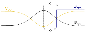
Assuming the QD potential is parabolic around the tip ( QD centre)(Dombrowski1999, ) while slowly varying in and to 0 far away from the tip, we approximate the tail of with an exponentially decaying function and assume the donor reservoir as homogeneous, normalized to 1 for , the distance between QD centre and reservoir edge, and 0 otherwise. This is schematically illustrated in Figure 8.
as is faster than . So as the QD approaches the reservoir i.e. increases, decreases and the current increases exponentially as measured.
.4 Calculation of the gate lever arm and additional capacitance ratios
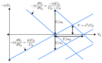
The two measured quantities and the bias lever arm can be deduced using only slopes from the Coulomb diagram pattern of the orthodox model for single-electron tunneling. This model is defined in terms of the source capacitance , the gate capacitance , the tip capacitance , and a stray capacitance (see Fig. 4a), and the total QD self-capacitance , and the stability diagram is shown in Fig. 9 from reference Hanson2007, .
First, from Fig. 9 we can deduce that for , the measured parameter corresponds to , which was experimentally determined to be . Second, from Fig. 9 we can also deduce that , which was experimentally determined to be , and . We can re-write the definition of the gate lever arm in terms of measured quantities and as follows:
which is equivalent to as discussed in the main text.
Additional capacitance ratios comparing the coupling between the QD and source, gate and tip are calculated (assuming negligible stray capacitance ) as follows:
References
- (1) Goldhaber-Gordon, D. et al. Kondo effect in a single-electron transistor. Nature 391, 156–159 (1998). URL https://doi.org/10.1038/34373.
- (2) Pekola, J. P. et al. Single-electron current sources: Toward a refined definition of the ampere. Reviews of Modern Physics 85, 1421–1472 (2013). URL https://link.aps.org/doi/10.1103/RevModPhys.85.1421.
- (3) Rossi, A. et al. An accurate single-electron pump based on a highly tunable silicon quantum dot. Nano Letters 14, 3405–3411 (2014). URL https://doi.org/10.1021/nl500927q.
- (4) Loss, D. & DiVincenzo, D. P. Quantum computation with quantum dots. Physical Review A 57, 120–126 (1998). URL https://link.aps.org/doi/10.1103/PhysRevA.57.120.
- (5) Kane, B. E. A silicon-based nuclear spin quantum computer. Nature 393, 133–137 (1998). URL http://dx.doi.org/10.1038/30156.
- (6) Petta, J. R. et al. Coherent Manipulation of Coupled Electron Spins in Semiconductor Quantum Dots. Science 309, 2180–2184 (2005).
- (7) Koppens, F. H. L. et al. Driven coherent oscillations of a single electron spin in a quantum dot. Nature 442, 766–771 (2006).
- (8) Feynman, R. P. Simulating physics with computers. International Journal of Theoretical Physics 21, 467–488 (1982). URL http://dx.doi.org/10.1007/BF02650179http://link.springer.com/article/10.1007%2FBF02650179.
- (9) Singha, A. et al. Two-Dimensional Mott-Hubbard Electrons in an Artificial Honeycomb Lattice. Science 332, 1176–1179 (2011).
- (10) Salfi, J. et al. Quantum simulation of the hubbard model with dopant atoms in silicon. Nat Commun 7, 11342 (2016). URL https://www.ncbi.nlm.nih.gov/pubmed/27094205.
- (11) Hensgens, T. et al. Quantum simulation of a fermi–hubbard model using a semiconductor quantum dot array. Nature 548, 70 (2017). URL http://dx.doi.org/10.1038/nature23022.
- (12) Kouwenhoven, L. P., Austing, D. G. & Tarucha, S. Few-electron quantum dots. Reports on Progress in Physics 64, 701 (2001). URL http://stacks.iop.org/0034-4885/64/i=6/a=201.
- (13) Hanson, R., Kouwenhoven, L. P., Petta, J. R., Tarucha, S. & Vandersypen, L. M. K. Spins in few-electron quantum dots. Reviews of Modern Physics 79, 1217–1265 (2007).
- (14) Zwanenburg, F. A. et al. Silicon quantum electronics. Reviews of Modern Physics 85, 961–1019 (2013).
- (15) Fuechsle, M. et al. A single-atom transistor. Nat Nanotechnol 7, 242–6 (2012). URL https://www.ncbi.nlm.nih.gov/pubmed/22343383.
- (16) Fölsch, S., Martínez-Blanco, J., Yang, J., Kanisawa, K. & Erwin, S. C. Quantum dots with single-atom precision. Nature Nanotech 9, 505–508 (2014).
- (17) Huff, T. et al. Binary atomic silicon logic. Nature Electronics 2019 2:4 1, 636–643 (2018).
- (18) He, Y. et al. A two-qubit gate between phosphorus donor electrons in silicon. Nature 571, 371–375 (2019). URL https://doi.org/10.1038/s41586-019-1381-2.
- (19) Yoo, M. J. et al. Scanning Single-Electron Transistor Microscopy: Imaging Individual Charges. Science 276, 579–582 (1997).
- (20) Sellier, H. et al. On the imaging of electron transport in semiconductor quantum structures by scanning-gate microscopy: successes and limitations. Semicond. Sci. Technol. 26, 064008 (2011).
- (21) Dombrowski, R., Steinebach, C., Wittneven, C., Morgenstern, M. & Wiesendanger, R. Tip-induced band bending by scanning tunneling spectroscopy of the states of the tip-induced quantum dot on InAs(110). Phys. Rev. B 59, 8043–8048 (1999).
- (22) Freitag, N. M. et al. Electrostatically confined monolayer graphene quantum dots with orbital and valley splittings. Nano Letters 16, 5798–5805 (2016). URL https://doi.org/10.1021/acs.nanolett.6b02548.
- (23) Salfi, J. et al. Valley filtering in spatial maps of coupling between silicon donors and quantum dots. Physical Review X 8, 031049 (2018). URL https://link.aps.org/doi/10.1103/PhysRevX.8.031049.
- (24) Shim, Y.-P., Ruskov, R., Hurst, H. M. & Tahan, C. Induced quantum dot probe for material characterization. Appl. Phys. Lett. 114, 152105 (2019).
- (25) Wagner, C. et al. Quantitative imaging of electric surface potentials with single-atom sensitivity. Nature Materials (2019). URL https://doi.org/10.1038/s41563-019-0382-8.
- (26) Malinowski, F. K. et al. Fast spin exchange across a multielectron mediator. Nat Comms 10, 1196 (2019).
- (27) Srinivasa, V., Xu, H. & Taylor, J. M. Tunable Spin-Qubit Coupling Mediated by a Multielectron Quantum Dot. Phys. Rev. Lett. 114, 226803 (2015).
- (28) Elzerman, J. M. et al. Single-shot read-out of an individual electron spin in a quantum dot. Nature 430, 431–435 (2004). URL <GotoISI>://WOS:000222801400036.
- (29) Bonet, E., Deshmukh, M. M. & Ralph, D. C. Solving rate equations for electron tunneling via discrete quantum states. Physical Review B 65, 045317 (2002). URL https://link.aps.org/doi/10.1103/PhysRevB.65.045317.
- (30) Hatem, L. et al. Scanning tunneling spectroscopy reveals a silicon dangling bond charge state transition. New Journal of Physics 17, 073023 (2015). URL http://stacks.iop.org/1367-2630/17/i=7/a=073023.
- (31) Salfi, J. et al. Spatially resolving valley quantum interference of a donor in silicon. Nat Mater 13, 605–10 (2014). URL https://www.ncbi.nlm.nih.gov/pubmed/24705384.
- (32) Taucer, M. et al. Single-electron dynamics of an atomic silicon quantum dot on the h-si(100)-(2 x 1) surface. Physical Review Letters 112, 256801 (2014). URL https://link.aps.org/doi/10.1103/PhysRevLett.112.256801.
- (33) Foxman, E. B. et al. Effects of quantum levels on transport through a coulomb island. Physical Review B 47, 10020–10023 (1993). URL https://link.aps.org/doi/10.1103/PhysRevB.47.10020.
- (34) Le, N. H., Fisher, A. J. & Ginossar, E. Extended Hubbard model for mesoscopic transport in donor arrays in silicon. Phys. Rev. B 96, 245406 (2017).
- (35) Le, N. H., Fisher, A. J., Curson, N. J. & Ginossar, E. Topological phases of a dimerized Fermi-Hubbard model (2019). eprint 1906.00488.