capbtabboxtable[][\FBwidth]
First Characterization of a Superconducting Filter-bank Spectrometer for Hyper-spectral Microwave Atmospheric Sounding with Transition Edge Sensor Readout.
Abstract
We describe the design, fabrication, integration and characterization of a prototype superconducting filter bank with transition edge sensor readout designed to explore millimetre-wave detection at frequencies in the range 40 to . Results indicate highly uniform filter channel placement in frequency and high overall detection efficiency. The route to a full atmospheric sounding instrument in this frequency range is discussed.
I Introduction
Superconducting on-chip filter-bank spectrometers (SFBSs) are a promising technology for a number of scientifically important applications in astronomy and meteorology that require low-noise, spectroscopic measurements at millimetre and sub-millimetre wavelengths. SFBSs are capable of achieving high channel counts and the individual channel characteristics such as shape, width, and position in frequency, power-handling and sensitivity can be tuned to the application. Moreover, the micro-fabrication techniques used in the production of these thin-film devices mean that SFBSs are intrinsically low-mass, physically compact and easily reproducible, making them well-suited for array applications for both ground-based and satellite-borne instruments. High signal detection efficiencies can be achieved up to the superconducting pair-breaking threshold of the superconductors used in the design; typically 680 GHz for Nb, but higher for superconducting compounds such as NbN or NbTiN.
Applications for astronomy include surveys of moderate red-shift galaxies () by precision determination of the frequencies of CO and rotational lines, multichroic pixels for cosmic microwave background (CMB) observations (foreground subtraction by observing in the Koopman et al. (2018) and atmospheric windows, and simultaneous observation in multiple CMB frequency bandsPan, Z., et al. (2018); Stebor, N., et al. (2016)) or observation of low-Z CO and O line emissions from nearby galaxies.Grimes, P. K., et al. Chip spectrometers coupling to superconducting kinetic inductance detectors (KIDs) are being developed by a number of groups and large multiplexing counts of order ’s have been demonstrated.Endo, Akira, et al. (2019); Redford, J, et al. (2018) However KID detectors are difficult to design for detection at low frequencies , the pair-breaking threshold for a typical low superconducting transition temperature material such as Al,Zhao et al. (2018a) and can also be challenging to calibrate as regards their power-to-output-signal responsivity. Superconducting transition edge sensors (TESs) are a type of bolometric detector where the power absorption is not limited by the pair-breaking threshold of a superconducting film. In addition their (power-to-current) responsivity is straightforward to determine both theoretically and experimentally. TES multiplexing schemes are a mature technology using both time- and frequency-domain approaches giving multiplexing factors of order ’s,Khosropanah et al. (2018); Henderson et al. (2016) and microwave TES readout schemes promise to equal the multiplexing factors demonstrated for KIDs.Henderson et al. (2018); Irwin et al. (2018)
Vertical profiles of atmospheric temperature and humidity measured by satellite-borne radiometric sounders provide vital information for long-range weather forecasting. These sounders work by measuring the upwelling radiance from the atmosphere in a number of spectral channels, typically either at microwave (MW) or infrared (IR) wavelengths. Vertical resolution and measurement accuracy improve rapidly with greater channel number and radiometric sensitivity.Aires et al. (2015); Dongre et al. (2018) Significant progress has been made in IR sounder performance; the Infrared Sounding Interferometer (IASI), for example, provides over eight thousand channels with sub-kelvin noise equivalent differential temperature (NETD).World Meteorological Organization However, while able to provide high quality data, IR sounders can do so only under infrequent clear-sky conditions, as clouds absorb and interfere with the signal of interest. MW sounders, by contrast, are not affected by cloud cover, but their use has been hampered by poorer instrument performance. Channel number is a significant problem: the Advanced Microwave Sounding Unit-A (AMSU-A) in current use has, for example, only fifteen channels,AIRS Project (2000) while the planned Microwave Imaging Instrument (MWI) will offer twenty-three.Alberti et al. (2012) Sensitivity is also an issue and a recent study by Dongre Dongre et al. (2018) has indicated that maintaining and/or improving sensitivity as channel count increases is vital. In this paper we report on an SFBS with TES readout as a technology for realising a MW sounding instrument with several hundred channels and sky-noise limited performance. This would represent a disruptive advance in the field, allowing measurements of comparable performance to IR sounders under all sky conditions.
The chip spectrometer reported here is a demonstrator for an atmospheric temperature and humidity sounder (HYper-spectra Microwave Atmospheric Sounding: HYMAS), that is being developed to operate at frequencies in the range .Dongre et al. (2018); Hargrave et al. (2017) The demonstrator was designed to cover the very important O2 absorption band at for atmospheric temperature sounding. We believe, however, that our prototype designs and initial characterizations are already relevant across the broad band of scientifically important research areas described above.
In Sec. II we give a brief overview of SFBSs and the particular features of the technology that make them attractive for this application. We will then describe the design of a set of devices to demonstrate the key technologies required for temperature sounding using the O2 absorption band at . In Sec. III we describe the fabrication of the demonstrator chips and their assembly with electronics into a waveguide-coupled detector package. In Sec. IV we report the first characterization of complete SFBS’s with TES readout detecting at , considering the TES response calibration, measurements of overall detection efficiency, and measurements of filter response. Finally we summarise the achievements and describe our future programme and the pathway from this demonstrator to a full instrument.
II Superconducting on-chip Filter-bank Spectrometers
 |
| Parameter | Specification | Units |
|---|---|---|
| Operating frequency range | 50–60 | GHz |
| Filter resolution | 100-500 | |
| Noise equivalent power | 3 | |
| Detector time constant | 5 | ms |
| Detector absorption efficiency | ||
| Background power handling | 60 | fW |
| Operating temperature | mK | |
| Number of channels | 35 |
In general, a filter-bank spectrometer uses a set of band-defining electrical filters to disperse the different spectral components of the input signal over a set of power detectors. In the case of an SFBS, the filters and detectors are implemented using microfabricated superconducting components, and are integrated together on the same device substrate (the ‘chip’). Integration of the components on the same chip eliminates housings, mechanical interfaces and losses between different components, helping to reduce the size of the system, while improving ruggedness and optical efficiency. In addition it is easy to replicate a chip and therefore a whole spectrometer, making SFBSs an ideal technology for realising spectroscopic imaging arrays.
Most mm- and sub-mm wave SFBSs that have been reported in the literature operate directly at the signal frequency, i.e. there is no frequency down-conversion step.Endo, Akira, et al. (2019); Redford, J, et al. (2018) There are two main benefits of this approach, the first of which is miniaturization. The size of a distributed-element filter is intrinsically inversely proportional to the frequency of operation: the higher the frequency, the smaller the individual filters and the more channels that can be fitted on the chip. The second benefit is in terms of instantaneous observing bandwidth, which is principle limited only by the feed for frequencies below the pair-breaking thresholds of the superconductors.
Operation at the signal frequency is made possible by: (a) the availability of superconducting detectors for mm- and sub-mm wavelengths, and (b) the low intrinsic Ohmic loss of the superconductors. Critically, (b) allows filter channels with scientifically useful resolution to be realised at high frequencies. In the case of normal metals, increases in Ohmic loss with frequency and miniaturisation of the components quickly degrade performance. As an example, the Ohmic losses in Nb microstrip line at sub-kelvin temperatures are expected to be negligible for frequencies up to 680 GHz Yassin and Withington (1995) (the onset of pair-breaking). The use of ultra-low noise superconductor detector technology such as TESs and KIDs, (a), in principle allows for extremely high channel sensitivities.
The SFBS test chips described here were developed with the target application of satellite atmospheric sounding and against the specification given in Table 1. Figure 1 shows the system level design of the chips. Each chip comprises a feeding structure that couples signal from a waveguide onto the chip in the range 45–65 GHz, followed by a filter-bank and a set of TES detectors. The chip is then housed in a test fixture that incorporates additional cold electronics and waveguide interfaces. In the sub-sections that follow we will describe the design of each of the components in detail.
Each of the test chips described has twelve detectors in total. This number was chosen for convenient characterisation without multiplexed readout, but the architecture readily scales to higher channel count. In principle the limiting factor is increasing attenuation on the feed line as more channels are added, but the losses on superconducting line are so low that other issues, such as readout capacity, are expected to be the main limit.
II.1 Feed and Transition
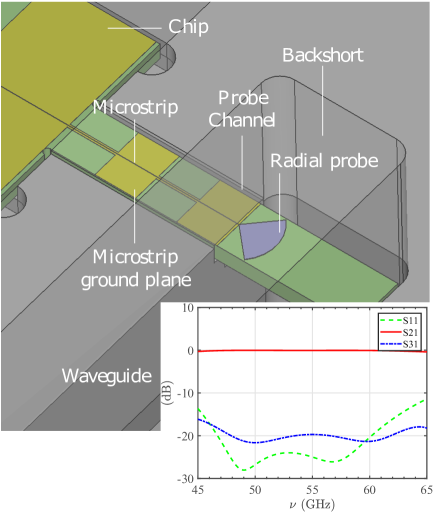 |
RF signal input to the test devices is via a standard 1.88 mm3.76 mm WR15 waveguide, allowing full coverage of the O2 band (WR15 has a recommended operating range of , single-mode operation from ). The signal is coupled from the waveguide onto a 22.3 microstrip line on the chip through a radial probe transition,Kooi et al. (2003) the design of which is shown in Fig. 2. A split block waveguide is used, the upper part of which has been rendered as transparent in the figure to allow the internal structure to be seen. A channel is machined through the waveguide wall at the split plane to accommodate a silicon beam extending from the chip, shown in green. This beam supports a fan-shaped radial probe, shown in blue, the apex of which connects to the upper conductor of the microstrip. The microstrip ground plane is shown in yellow. Not visible is an air channel under the beam, which raises the cut-off frequency of the waveguide modes of the loaded channel above the band of operation.
It is critical for performance that the ground plane is at the same potential as the waveguide/probe-channel walls at the probe apex, however it is not straightforward to make a physical connection. The changes in ground plane width shown in Fig. 2 implement a stepped impedance filter in the ground-plane/wall system to ensure a wideband short at the probe plane, assuming the ground plane is wire-bonded to the walls in the chip cavity. This filter also prevents power flow along the air channel due to the TEM mode.
The performance of the design was simulated using OpenEMS, a finite difference time domain (FDTD) solver.Liebig Insertion loss (), reflection loss () and indirect leakage to the chip cavity () as a function of frequency are shown in the inset of Fig. 2. As can be seen, the design achieves better than -3 dB insertion loss over , corresponding to a fractional bandwidth of nearly 35 %.
II.2 Filter-bank

The filter-bank architecture employed on the test chips is shown schematically in Fig. 3(a). It comprises ten half-wave resonator filters driven in parallel from a single microstrip feed line. Each of the filters comprises a length of microstrip line, the ends of which are connected by overlap capacitors to the feed and an output microstrip line. The output line is terminated by a matched resistor that is closely thermally-coupled to a TES bolometer. Both the termination resistor and TES are thermally isolated from the cold stage. The feed line itself is terminated on an eleventh matched resistor coupled to a TES. This TES measures the power remaining after passing the filter bank and is subsequently described as the residual power detector. This TES was specifically designed to handle the expected higher incident power. A twelfth detector on chip has no microwave connection and was used as a ‘dark’ (i.e. nominally power-free) reference. A common superconducting microstrip design is used for all parts of the filter-bank, consisting of a Nb ground plane, a 400 nm thick SiO2 dielectric layer and a 3 m wide, 500 nm thick, Nb trace. The modelled characteristic impedance is 22.3 .Yassin and Withington (1995)
The spectral characteristics of each filter are determined by the resonant behaviour of the line section and the strength of the coupling to the feed and detector. For weak coupling, the line section behaves as an open-ended resonator and transmission peaks sharply at resonance.
Each filter channel is designed to have its own fundamental frequency . For a filter of length and phase velocity , is given by
| (1) |
Tuning over the range is achieved by values of in the range . The channel resolution where is the 3-dB width.
The bandwidth of a filter and its peak-value of transmission are governed by losses in the resonator, as measured by the quality factor. Assuming power loss from the resonator when the stored energy is , the total quality factor of the resonator (and hence the resolution of the filter ) is defined by . can be further decomposed into the sum of the power loss and to the input and output circuit respectively (coupling losses) and the power dissipated in the resonator itself through Ohmic and dielectric loss (internal losses). We can then define additional quality factors , and by These correspond to the Q-factor of the resonator in the limit where the individual losses are dominant, and . With these definitions, the power gain of the channel as a function of frequency can be shown to be
| (2) |
and are controlled by the input and output coupling capacitors. For maximum transmission of power to the filter channel detector (-3 dB) we must engineer , in which case . Therefore the minimum achievable bandwidth is limited by . Under the same conditions the power transmitted to the residual power detector is
| (3) |
and the power is reduced by 6-dB on resonance as seen from the dotted black line in Fig. 3(b). In practice the presence of the coupling capacitors causes the measured centre frequency of the filter to differ slightly from the resonant frequency of the open-ended line, as given by (1). The detuning is dependent on coupling strength and analysis of the perturbation of the circuit to first-order gives
| (4) |
Ohmic loss is small in superconducting microstrip lines at low temperatures. Instead, experience with superconducting microresonators 10 GHz suggests dielectric loss due to two-level-systems will govern . Zmuidzinas (2012) A main aim of the prototype devices was to investigate the loss mechanisms active at millimetre wavelengths, although extrapolation from the low-frequency data suggests spectral resolutions of a few hundred should be easily achievable for the microstrip design used here, and higher may be achievable for alternatives such as coplanar waveguide.
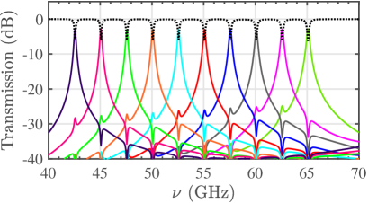
We report on two of the four different filter bank designs that were fabricated on the demonstrator devices. Three of these have identically spaced channels, designed to be 2.5 GHz apart over the range . The designs differ in spectral resolution of the channels, with target values of 250, 500 and 1000. These explore the achievable control of channel placement and resolution and provide experimental characterization of the millimetre-wave properties of the microstrip over a wide frequency range. However, the channels in these designs are widely spaced. The fourth design investigated an alternate possible mode of operation where the passbands of the filters overlap significantly, with nine channels in the band . In this case the spacing of the filters along the feed line becomes significant, as the filters interact with each other electrically. If the filters are arranged in order of decreasing frequency and placed approximately a quarter of a wavelength apart, part of the in-band signal scattered onto the feed by the filter is reflected back in phase from the next filter along, enhancing transmission to the detector. Consequently the transmission of the filters can be increased by dense packing, but at the expense of the shape of the response; we are investigating the implications for scientific performance. The modelled passbands for the widely-spaced filter banks are shown in Fig. 3(b).
II.3 TES design
Electrothermal feedback (ETF) in a thermally-isolated TES of resistance , voltage-biased within its superconducting-normal resistive transition means that the TES self-regulates its temperature very close to , the TES transition temperature.Irwin and Hilton (2005) When the superconducting-normal resistive transition occurs in a very narrow temperature range , where characterizes the transition sharpness. Provided the bath temperature, the small-signal power-to-current responsivity is then given by . Here , and are the TES temperature, current and resistance respectively at the operating point and is the load resistance. All are simple to evaluate from measurements of the TES and its known bias circuit parameters meaning that is straightforward to evaluate.
The TESs we report on were designed to operate from a bath temperature of in order to be usable from a simple cryogenic cooling platform, to have a saturation power of order to satisfy expected power loading, and a phonon-limited noise equivalent power (NEP) of order to minimise detector NEP with respect to atmospheric noise (see Table 1). TES design modelling indicates that the required performance should be achievable with a superconducting-normal transition temperature . The detailed calculation depends on the value of the exponent that occurs in the calculation of the power flow from the TES to the heat bath: , where is a material dependent parameter that includes the geometry of the thermal link between the TES and bath. For ideal voltage bias () the saturation power is and is the TES normal-state resistance.Irwin and Hilton (2005) Under typical operating conditions . The thermal conductance to the bath , determines the phonon-limited NEP where , is Boltzmann’s constant, and takes account of the temperature gradient across . Our previous work suggests that at the operating temperature and length scales should apply for 200-nm thick at these temperatures with lengths . For the filter channels, thermal isolation of the TES was formed from four 200nm-thick legs each of length , three of width and one of to carry the microstrip. The residual power detector had support legs of length and the same widths as for the filter channels.
III Fabrication and Assembly
The detector chips were fabricated on -thick Si wafers coated with a dielectric bilayer comprising 200 nm thick low-stress and an additional 50 nm etch stop. After Deep Reactive Ion Etching (DRIE) the , films formed the thermal isolation structure. The detectors were made by sputtering metal and dielectric thin films in ultra-high vacuum. The superconducting microstrip was formed from a 150 nm-thick Nb ground plane with 400 nm amorphous silicon dioxide () dielectric and a 400 nm-thick -wide Nb line. Coupling capacitors were made from and Nb. Thin film AuCu resistors terminate the microstrip on the TES island. The TESs were fabricated from TiAl bilayers with the Ti and Al thicknesses of thicknesses 150 nm, 40 nm respectively, calculated to target a superconducting transition temperature of .Zhao et al. (2018b) Electrical connections to the TES were sputtered Nb. DRIE removed the Si under the TES such that the island and legs provide the necessary thermal isolation. The DRIE also released the individual chips from the host wafer and defined the chip shape seen in 4.
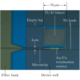
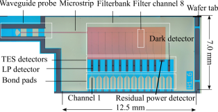
Figure 4(a) shows an image of the residual-power detector prior to DRIE of the Si. The -wide leg supporting the microstrip is indicated in the lower left-hand region of the image. The AuCu termination can be seen. Figure 4 (b) shows a composite high resolution photograph of a completed detector chip after DRIE. The component structures, waveguide probe, filter-bank, TES detectors and superconducting contact pads are indicated. The individual filter channels are also visible. Filter lengths are determined by the small coupling capacitors that are (just) visible as darker dots between the through-line and the individual TES wells, the lengths increase with channel number (left-to-right in the image) and correspondingly reduces.
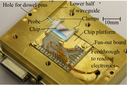 |
Figure 5 shows an image of a completed chip mounted in a detector enclosure. The probe can be seen extending into the lower half of the split waveguide. Al wirebonds connect the chip ground plane to the enclosure and on-chip electrical wiring to the superconducting fan-out wiring. Superconducting NbTi wires connect through a light-tight feed-through into the electronics enclosure on the back of the detector cavity. The low-noise two-stage SQUIDs used here were provided by Physikalisch-Technische Bundesanstalt (PTB). The upper section of the detector enclosure completed the upper section of the waveguide and ensured that the package was light-tight. Completed detector packages were cooled using two separate cryogen-cooled ADR’s both giving a base temperature .
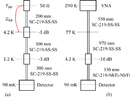 |
Figure 6 (a) shows a schematic of the blackbody power calibration scheme. A matched resistive load (Fairview Microwave SKU:ST6510)Infinite Electronics International, Inc. terminated a length of Coax Co. Ltd SC-219/50-SS-SS coaxial line.Coax Co. Ltd. The load was mounted on a thermally isolated Cu plate within the cryostat vacuum space. This termination-resistor stage was equipped with a calibrated LakeShore RuOx thermometerLake Shore Cryotronics, Inc. and resistive heater and was connected to the refrigerator stage by a length of copper wire (, ) that determined the dominant stage time constant which was estimated at . Further SC-219 connected the termination resistor to a 3-dB attenuator (Fairview Microwave SA6510-03) mounted on the stage itself, to a further attenuator mounted on the stage, in order to minimise heat-loading to the cold-stage by heat-sinking the inner coax conductor, and then to the WR-15 coax-waveguide transition (Fairview Microwave SKU:15AC206), waveguide probe and detector chip. The total coax length was . Results of these measurements are reported in Sec. V.
The spectral response of the filters was measured using a continuous wave (CW) source. For these tests a different cryostat was used, but it again comprised a two-stage (1K/50mK) ADR launched from a 4 K plate cooled by liquid cryogens. A different set cold electronics with nine single-stage SQUIDs, provided by PTB was used that allowed simultaneous readout of nine devices.
Figure 6 (b) shows a schematic of the scheme. A Rohde & Schwarz ZVA-67 VNA capable of measurements up to was used as a frequency-tuneable, power-levelled, CW source and the signal coupled down to the detector block on coaxial cable. A KMCO KPC185FF HA hermetic feedthrough was used to enter the cryostat, then 1520 mm of Coax Co. Ltd SC-219/50-SS-SS coaxial cable was used for the connection between room temperature and the plate, anchoring on the liquid nitrogen tank, liquid helium tank and finally the plate itself. The final connection from to the waveguide adapter on the test block was made using 330 mm of Coax Co. Ltd SC-219/50-NbTi-NbTi superconducting cable for thermal isolation. A 10 dB attenuator (Fairview Microwave SA6510-10) was inserted in line at the plate to provide thermal anchoring between the inner and outer conductors of the coaxial cable and isolation of the detectors chip from short-wavelength power loading. All connections were made with 1.85 mm connectors to allow mode free operation up to . Measurements indicated the expected total attenuation of order 68 dB between room temperature and the WR-15 waveguide flange. In operation the frequency of the CW source was stepped through a series of values and the output of the devices logged in the dwell time between transitions, exploiting the normal mode of operation of the VNA. Results of these measurements are reported in Sec. VI.
Two chips were characterized in this series of tests. Both chips were fabricated on the same wafer, but have different designed filter resolving powers. Chip 1 has filters designed with was used for the blackbody measurements with measurements on filter channels 4-6, 11 (the residual power detector), and 12 (the dark detector). Chip 2 with was used for the spectral measurements and we report measurements on channels 3-8, 10 and 12. Both chips were designed to cover the range.
IV Results
IV.1 TES characteristics
| Channel | Notes | ||||
|---|---|---|---|---|---|
| 4 | 2.6 | 457 | Filter | ||
| 5 | 2.5 | 452 | Filter | ||
| 6 | 2.4 | 454 | Filter | ||
| 12 | 2.4 | 455 | Dark | ||
| 11 | 2.4 | 459 | Residual | ||
| Power |
Table 2 shows measured and calculated values for the DC characteristics of 5 channels from Chip 1. was close-to but somewhat lower than designed, and was higher. The critical current density was also reduced from our previously measured values even for pure Ti films. This may indicate that these TESs demonstrate the thin-film inter-diffusion effect between Ti-Nb couples recently reported by Yefremenko et al..Yefremenko et al. (2018) The superconducting-normal resistive transition with , as inferred from measurements of the TES Joule power dissipation as a function of bias voltage, appeared somewhat broad. Hence, was determined from the power dissipated at constant TES resistance , close to the bias voltage used for power measurements. The exponent in the power flow was for all TESs.
IV.2 TES ETF parameters and power-to-current sensitivity estimate
 |
For a TES modelled as single heat capacity with conductance to the bath , the measured impedance is given byIrwin and Hilton (2005)
| (5) |
where is the load resistance, is the input inductance of the SQUID plus any stray inductance, is the TES impedance and is the measurement frequency. The TES impedance is given by
| (6) |
where . is the Joule power at the bias point, is the operating temperature and characterizes the sharpness of the resistive transition at the bias point. measures the sensitivity of the transition to changes in current . At measurement frequencies much higher than the reciprocal of the effective TES time (here taken to be ), , and so can be determined with minimal measured parameters. At low frequencies, here taken to be , , so that and hence can be found. The low frequency power-to-current responsivity is given by
| (7) |
For a TES with good voltage bias , and a sharp transition , then provided , and the power-to-current responsivity is straight-forward to calculate. For the TiAl TES reported here the measured power-voltage response suggested a fairly broad superconducting-normal transition. Here we use the full expression given by Eq. 7 with and the calculated value of the reciprocal within the brackets.
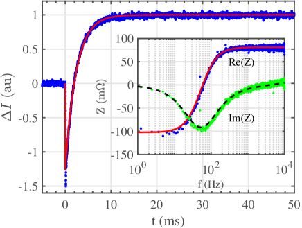
The inset of Fig. 7 shows the measured real and imaginary parts (blue and green dots respectively) of the impedance of the residual power detector, channel 11. The solid red and dashed black lines show the modelled impedance. Table 3 shows the derived ETF parameters and heat capacity. The main figure shows the measured normalised TES current response (blue dots) to a small change in TES bias voltage (i.e. a small modulation of instantaneous Joule power), and (red line) the calculated response using the parameters determined in modelling the impedance. No additional parameter were used.
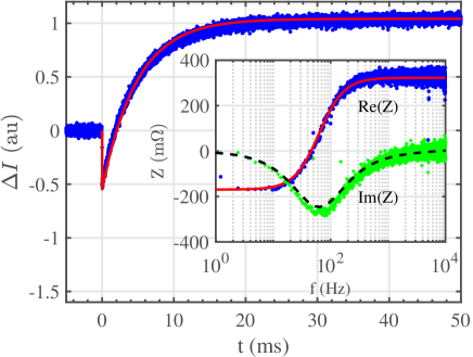 |
The inset of Fig. 8 shows the measured real and imaginary parts (blue and green dots respectively) of the impedance of the dark detector, channel 12. The solid red and dashed black lines show the modelled impedance. Table 3 shows the derived ETF parameters and heat capacity. The main figure shows the measured normalised TES current response (blue dots) to a small change in TES bias voltage (i.e. a small modulation of instantaneous Joule power), and (red line) the calculated response using the parameters determined in modelling the impedance. As in the modelling shown in Fig. 7, no additional parameter were used. Comparable correspondence between measured impedance and current step response using impedance-derived ETF parameters and heat capacity was found for all measured channels.
| Channel | Notes | ||||
|---|---|---|---|---|---|
| 4 | 66 | 1.3 | 220 | 0.77 | Filter |
| 5 | 77 | 2.9 | 200 | 0.74 | Filter |
| 6 | 114 | 4.4 | 200 | 0.80 | Filter |
| 12 | 128 | 1.3 | 180 | 0.88 | Dark |
| 11 | 114 | 1.9 | 390 | 0.66 | Residual |
| Power |
V Power calibration
V.1 Available in-band power
We assume that the matched termination load, waveguide and probe behave as an ideal single-mode blackbody source at temperature with a bandwidth determined by the waveguide cut-on and probe 3-dB cut-offs giving a top-hat filter with minimum and maximum transmission frequencies , respectively. Fitting a model to the manufacturer’s data we find that loss in the coax can be described by , where is the total line length. Additional losses arise from the 3-dB attenuators that form the coax heat-sinks (2 being used), and the connectors (8 in total), each contributing an additional loss of . The total attenuation (in dB) is then
| (8) |
The change in available power at the probe is , with the lowest operating temperature for the blackbody and
| (9) |
where is the Bose distribution, and is Planck’s constant.
To calculate the power transmission to the residual power detector, we assume each of the filter channels of centre frequency , (where identifies the channel and ) taps its maximum fraction of the incident power given by Eq. 2 and the transmitted power is given by Eq. 3, with attenuation at the residual power detector due to each filter at its resonant frequency. The total available power at the residual power detector is
| (10) |
is the product and is the overall efficiency referenced to the input to the probe.
 |
V.2 Coupled power measurement
Measurements of the detection efficiency were made on Chip 1 with the cold stage temperature maintained at using a PID feedback loop to regulate the ADR base temperature. Under typical (unloaded) conditions the cold stage temperature is constant at . was increased by stepping the blackbody heater current at with the change in measured TES current and digitized at . Changes in detected power in both the residual power and dark detectors as was increased were calculated from the change in their respective measured currents assuming the simple power-to-current responsivity, , with the TES operating points calculated from measured and known electrical circuit parameters. At the highest used, , increased by suggesting power loading onto the cold stage. Under the same blackbody loading, and even after subtracting the expected dark detector power response due to , , the dark detector indicated a current (hence power) response that we interpret here as additional incident power. We modelled this residual response as a change in the temperature of the Si chip itself , finding an increase of order at the highest . The modelled chip response closely followed a quadratic response with . Although the origins of this additional power loading could not be determined in this work, it may have arisen from residual short wavelength loading from the blackbody source. At 10 K the peak in the multimode blackbody spectrum is around implying that there may be a significant available detectable power at high frequencies. Even a very small fraction of this power would be sufficient to produce the inferred chip heating. Changes in detected power for the residual power detector with were accordingly reduced, to include the effect of both the measured , and the modelled .
Figure 9 shows the change in detected power as a function of , for in the range 4.2 to . The power response is close to linear with temperature (the correlation coefficient ). The inset shows the maximum available power calculated for three values of the filter resolution , and - the designed value. The residual power increases as increases. As discussed in Sec. VI the designed value may represent an over-estimate of the achieved for the measured chip. Assuming we estimate an efficiency of and the lower error is calculated assuming the designed filter resolution . The measured power and hence efficiency estimate were calculated assuming the maximum power-to-current responsivity . From the measured response of the residual power detector described in Sec. IV.2, and Table 3 we see that this over-estimates the sensitivity by a factor . Taking account of this correction, our final estimate of overall efficiency referred to the input to the probe is increased to .
VI Filter spectral response
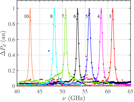 |
Measurements of the spectral response were made on Chip 2. Figure 10 shows (dots) the normalised power detected and (solid lines) the modelled response using Eq. 2 (i.e. a Lorentzian) for filter channels 3 to 8 and 10 as labelled. Colours and annotation identify the individual channels. The individual filter responses and are shown in Table 4 along with the nominal design filter centre frequencies. Errors in were calculated from the fit to the data. The frequency sampling of channel 10 was insufficient to determine the filter response. For this channel the model fit shown was calculated assuming (the mean of the other channels) and is plotted only as a guide to the eye. For this series of measurements, within measurement noise, there was no observable response in the dark channel and we estimate . The absence of any detectable dark response using a power-levelled, narrow-band, source operating at a fixed temperature of – in which case we might expect no, or only very small changes in additional loading – gives weight to our interpretation and analysis that the blackbody and efficiency measurements should indeed be corrected for heating from a broad-band, temperature modulated source. In those measurements the dark detector showed an unambiguous response.
| Channel | |||
|---|---|---|---|
| 3 | 60.0 | ||
| 4 | 57.5 | ||
| 5 | 55.0 | ||
| 6 | 52.2 | ||
| 7 | 50.0 | ||
| 8 | 47.5 | ||
| 10 | 42.5 |
The shapes of the individual filter responses were close to the expected Lorentzian as shown in more detail in Fig 11 for channels 3 and 5.
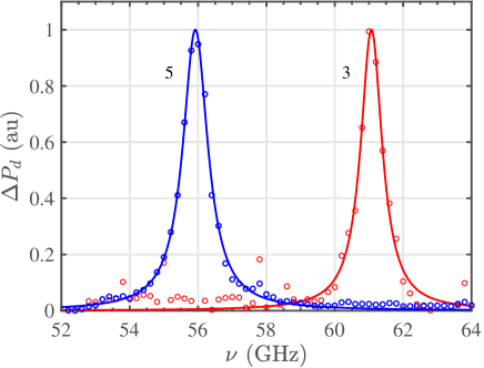 |
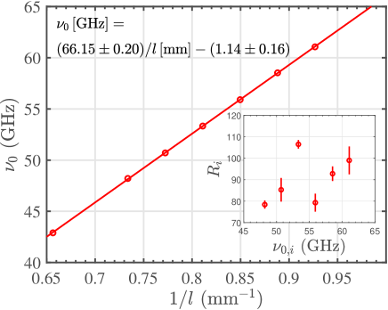
Figure 12 shows the measured filter centre frequencies as a function of reciprocal filter length . The correlation is close to unity () as predicted by Eqs. 1 and 4, demonstrating the precision with which it is possible to position the individual filter channels. From the calculated regression line , and assuming a modest lithographic precision of for the fabrication process, we calculate for a 50 GHz filter, or . The finite value for the intercept is unexpected and is an area for future investigation. Uncertainties in parameters such as the realised coupling capacitance and the exact permittivity of the dielectric constant are expected, but from Eqs. [1] and [4], should only affect the constant of proportionality in the relationship , rather than generate an offset. Instead, the offset suggests an issue with some detail of the underlying circuit model.
 |
VII Summary and Conclusions
We have described the design, fabrication and characterization of a superconducting filter bank spectrometer with transition edge sensor readout. We have described the design of a waveguide-microstrip radial probe transition with wide bandwidth. We have demonstrated detection of millimetre-wave radiation with frequencies from 41 to 64 GHz with characteristics that are already suitable for atmospheric temperature sounding using the O2 absorption band. The temperature of a cryogenic blackbody was modulated to determine the power detection efficiency of these prototype devices, finding an efficiency using the measured impedance of the TES to determine the detection responsivity. Filter profiles were determined on a separate device. The measured channel profiles were Lorenztian as expected. We measured extremely good predictability of relative channel placement, and also in individual channel placement . We found somewhat lower filter resolutions than the designed values, possibly arising from our use in the filter design of dielectric constant measurements at lower frequencies compared to those explored here or, perhaps, unexpected dielectric losses. This will be an area for future investigation. In the next phase of this work we will continue to investigate this question but also investigate alternative filter architectures – particularly coplanar structures where dielectric losses may-well be lower. Guided by the measurements reported, we will refine our designs to increase channel density for the O2-band observations and also include higher frequency channels particularly aimed at observation of the 183 GHz water-vapor line to enable a complete on-chip atmospheric temperature and humidity sounding instrument. Finally we emphasize that, although we have presented and discussed these measurements in the context of an enhanced atmospheric temperature sounding demonstrator, we believe we have already shown impressive spectroscopic and low-noise power detection at technically challenging millimetre-wave frequencies, with applications across a broad spectrum of scientific enquiry.
VIII Acknowledgements
This work was funded by the UK CEOI under Grant number RP61060435A07.
References
- Koopman et al. (2018) B. J. Koopman et al., “Advanced ACTPol Low-Frequency Array: Readout and Characterization of Prototype 27 and 39 GHz Transition Edge Sensors,” J. Low Temp Phys 193, 1103–1111, Unique–ID = ISI:000451734500059, DOI = 10.1007/s10909–018–1957–5 (2018).
- Pan, Z., et al. (2018) Pan, Z., et al., “Optical Characterization of the SPT-3G Camera,” J. Low Temp. Phys. 193, 305–313 (2018).
- Stebor, N., et al. (2016) Stebor, N., et al., “The Simons Array CMB Polarization Experiment,” in Millimeter, Submillimeter, and Far-infrared Detectors and Instrumentation for Astronomy VIII, Procs. SPIE, Vol. 9914, edited by Holland, WS and Zmuidzinas, J (2016).
- (4) Grimes, P. K., et al., “Instrumentation for single-dish observations with the Greenland Telescope,” in Millimeter, Submillimeter, and Far-Infrared Detectors and Instrumentation for Astronomy VII, Procs. SPIE, edited by Holland, WS and Zmuidzinas, J, p. 91531V.
- Endo, Akira, et al. (2019) Endo, Akira, et al., “Wideband on-chip terahertz spectrometer based on a superconducting filterbank,” J. Astron. Telesc. Inst. 5 (2019), 10.1117/1.JATIS.5.3.035004.
- Redford, J, et al. (2018) Redford, J, et al., “The Design and Characterization of a 300 channel, optimized full-band Millimeter Filterbank for Science with SuperSpec,” in Millimeter, Submillimeter, and Far-infrared Detectors and Instrumentation for Astronomy IX, Procs. SPIE, Vol. 10708, edited by Zmuidzinas, J and Gao, JR (2018).
- Zhao et al. (2018a) S. Zhao, D. J. Goldie, S. Withington, and C. N. Thomas, “Exploring the performance of thin-film superconducting multilayers as kinetic inductance detectors for low-frequency detection,” Supercond. Sci. Technol. 31 (2018a), 10.1088/1361-6668/aa94b7.
- Khosropanah et al. (2018) P. Khosropanah, E. Taralli, L. Gottardi, C. P. de Vries, K. Nagayoshi, M. L. Ridder, H. Akamatsu, M. P. Bruijn, and J. R. Gao, “Development of TiAu TES X-ray calorimeters for the X-IFU on ATHENA space observatory,” in Space Telescopes and Instrumentation 2018: Ultraviolet to Gamma Ray, Proc. SPIE, Vol. 10699, edited by DenHerder, JWA and Nikzad, S and Nakazawa, K (2018).
- Henderson et al. (2016) S. W. Henderson et al., “Advanced ACTPol Cryogenic Detector Arrays and Readout,” J. Low Temp. Phys. 184, 772–779 (2016).
- Henderson et al. (2018) S. W. Henderson et al., “Highly-multiplexed microwave SQUID readout using the SLAC Microresonator Radio Frequency (SMuRF) Electronics for Future CMB and Sub-millimeter Surveys,” in Millimeter, Submillimeter, and Far-Infrared Detectors and Instrumentation for Astronomy IX, Procs. SPIE, Vol. 10708 (2018).
- Irwin et al. (2018) K. D. Irwin, S. Chaudhuri, H. M. Cho, C. Dawson, S. Kuenstner, D. Li, C. J. Titus, and B. A. Young, “A Spread-Spectrum SQUID Multiplexer,” J. Low Temp. Phys. 193, 476–484 (2018).
- Aires et al. (2015) F. Aires, C. Prigent, E. Orlandi, M. Milz, P. Eriksson, S. Crewell, C.-C. Lin, and V. Kangas, “Microwave hyperspectral measurements for temperature and humidity atmospheric profiling from satellite: The clear-sky case,” Journal of Geophysical Research: Atmospheres 120, 11–334 (2015).
- Dongre et al. (2018) P. K. Dongre, S. Havemann, P. Hargrave, A. Orlando, R. Sudiwala, S. Withington, C. Thomas, and D. Goldie, “Information content analysis for a novel TES-based Hyperspectral Microwave Atmospheric Sounding Instrument,” in Remote Sensing of Clouds and the Atmosphere XXIII, Procs. SPIE, Vol. 10786, edited by Comeron, A and Kassianov, EI and Schafer, K and Picard, RH and Weber, K (2018) p. 1078608.
- (14) World Meteorological Organization, “OSCAR Instrument Guide: IASI,” https://www.wmo-sat.info/oscar/instruments/view/207.
- AIRS Project (2000) AIRS Project, “Algorithm Theoretical Basis Document Level 1b, Part 3: Microwave Instruments,” Online: https://microwavescience.jpl.nasa.gov/files/mws/ATBD-MW-21.pdf (2000).
- Alberti et al. (2012) G. Alberti, A. Memoli, G. Pica, M. Santovito, B. Buralli, S. Varchetta, S. d’Addio, and V. Kangas, “Two microwave imaging radiometers for metop second generation,” in 2012 Tyrrhenian Workshop on Advances in Radar and Remote Sensing (TyWRRS) (IEEE, 2012) pp. 243–246.
- Hargrave et al. (2017) P. Hargrave, S. Withington, S. A. Buehler, L. Kluft, B. Flatman, and P. K. Dongre, “THz spectroscopy of the atmosphere for climatology and meteorology applications,” in Next-Generation Spectroscopic Technologies X, Procs. SPIE, Vol. 10210, edited by Druy, MA and Crocombe, RA and Barnett, SM and Profeta, LTM (2017).
- Yassin and Withington (1995) G. Yassin and S. Withington, “Electromagnetic models for superconducting millimetre-wave and sub-millimetre-wave microstrip transmission lines,” Journal of Physics D: Applied Physics 28, 1983–1991 (1995).
- Kooi et al. (2003) J. Kooi, G. Chattopadhyay, S. Withington, F. Rice, J. Zmuidzinas, C. Walker, and G. Yassin, “A full-height waveguide to thin-film microstrip transition with exceptional RF bandwidth and coupling efficiency,” International Journal of Infrared and Millimeter Waves 24, 261–284 (2003).
- (20) T. Liebig, “openEMS - Open Electromagnetic Field Solver,” https://github.com/thliebig/openEMS-Project.
- Zmuidzinas (2012) J. Zmuidzinas, “Superconducting microresonators: Physics and applications,” Annu. Rev. Condens. Matter Phys. 3, 169–214 (2012).
- Irwin and Hilton (2005) K. D. Irwin and G. C. Hilton, “Transition-edge sensors,” in Cryogenic Particle Detection, Topics in Applied Physics, edited by C. Enss (Springer, Berlin, 2005) pp. 63–149.
- Zhao et al. (2018b) S. Zhao, D. J. Goldie, C. N. Thomas, and S. Withington, “Calculation and measurement of critical temperature in thin superconducting multilayers,” Supercond. Sci. Technol. 31 (2018b), 10.1088/1361-6668/aad788.
- (24) Infinite Electronics International, Inc., https://www.fairviewmicrowave.com/.
- (25) Coax Co. Ltd., http://www.coax.co.jp/en/product/sc/219-50-ss-ss.
- (26) Lake Shore Cryotronics, Inc. , https://www.lakeshore.com/.
- Yefremenko et al. (2018) V. Yefremenko et al., “Impact of Electrical Contacts Design and Materials on the Stability of Ti Superconducting Transition Shape,” J. Low Temp. Phys. 193, 732–738 (2018).