A Single-Quantum-Dot Heat Valve
Abstract
We demonstrate gate control of electronic heat flow in a thermally-biased single-quantum-dot junction. Electron temperature maps taken in the immediate vicinity of the junction, as a function of the gate and bias voltages applied to the device, reveal clearly defined Coulomb diamond patterns revealing a maximum heat transfer right at the charge degeneracy point. The non-trivial bias and gate dependence of this heat valve results from both the quantum nature of the dot at the heart of device and its strong coupling to leads.
pacs:
73.23.HkIn the emerging field of quantum thermodynamics, heat transport and dissipation in a quantum electronic device is a fundamentally important topic Pop2010 ; Lee2013 ; Zotti2014 ; Dubi2011 . Gate-tunable single-quantum dot junctions Kouwenhoven2001 are paradigmatic test benches for quantum transport. Whereas the study of charge transport therein has already allowed the exploration of a large palette of physical effects at play, heat transport and thermoelectric properties have been investigated in a limited number of cases, e.g. in quantum dots formed in a two-dimensional electron gas (2DEG) Scheibner2005 ; Dzurak1997 ; Godijn1999 and in semiconducting nanowires Josefsson2018 ; Jaliel-PRL19 ; Prete-NanoLett19 . As opposed to charge transport processes, the understanding of electronic heat transport and generation across a nano-scale object is, experimentally, still in its infancy Kim2001 ; Huang2007 ; Tsutsui2008 . Local thermometry has been achieved only in a very limited number of quantum devices. The temperature dependence of the critical current of a superconducting weak link was used in scanning probe experiments to reveal for instance the scattering sites in high-mobility graphene Halbertal2016 ; Marguerite2019 . Yet, to date, these experiments are limited to temperatures above 1 K. At milliKelvin temperatures, local thermometry can be performed in quantum devices formed in a 2DEG by a variety of methods Molenkamp1992 ; Prance-PRL09 that have recently been pushed to quantitative accuracy Jezouin2013 ; Sivre2018 ; Banerjee2018 . Noise thermometry was applied to thermoelectric measurements in InAs nanowires Tikhonov2016 . In metallic devices, electronic thermometry is usually based on the temperature dependence of charge transport in superconducting hybrids, either in the tunnelling regime for Normal metal-Insulator-Superconductor (NIS) junctions Giazotto-RMP ; Nahum1995 or at higher transparencies allowing for superconducting correlations Meschke-JLTP09 ; WangAPL18 ; Giazotto-Nature12 . This has recently allowed the realization of a photonic heat valve with a superconducting qubit coupled to heat reservoirs (probed by NIS probes) through coplanar waveguide resonators Ronzani-NatPhys18 .
The single electron transistor (SET) is an essential brick for the emerging field of quantum caloritronics Saira2007 . Building on the NIS thermometry technique, the thermal conductance of a metallic SET was measured Dutta-PRL17 . Despite the continuous density of states in the metallic island, electron interactions readily lead to striking deviations from the Wiedemann-Franz law Kubala-PRL08 . Going beyond this simple case, two questions arise: (i) how does such a SET behave thermally beyond equilibrium, that is, at finite voltage bias and/or at large temperature difference where both Joule heat and heat transport are to be taken into account, and (ii), if the central island is replaced by a quantum dot (), how would the discrete nature of its energy spectrum manifest in the thermal properties of the device? In the weak coupling regime, the discreteness of the QD energy spectrum makes electronic transport processes strongly selective in energy. At zero net particle current, whatever the gate voltage, the heat flow is zero since electrons tunnel back and forth exactly at the energy level defined by the QD. The heat conductance is thus zero at all gate voltages. Heat transfer is predicted only at non-zero particle current, when the QD energy level is positioned just above or below the Fermi level of the hot lead, so that high-energy electrons can escape through the dot, or low-energy electrons can be injected there Edwards-APL93 ; Prance-PRL09 .
In this Letter, we report on the operation of a single-quantum-dot heat valve. The methodological novelty is to introduce local thermometry in a metallic single quantum dot device. When current flows through it, Joule dissipation results in a temperature increase following the usual Coulomb diamonds’ pattern. At zero net charge current and charge degeneracy, the observed electronic heat transfer is the result of energy quantization in the dot combined with strong tunnel coupling to the leads.
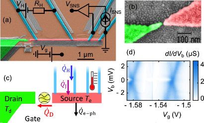
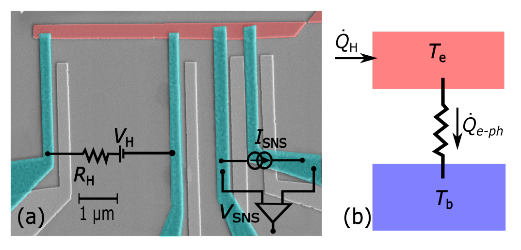
Figures 1(a,b) display a colored scanning electron micrograph of a typical device as the one reported here, whereas Fig. 1(c) shows a thermal diagram of the same, with the corresponding color code for each device element. The device is different from that in Ref. Dutta-Nanolett19 but it has the same geometry and the fabrication procedure is similar. The fabrication of the main part of the device is based on e-beam lithography, three-angle, Au thin film evaporation and lift-off. After the lift-off, we deposit a 1-2 nm thin Au layer on top of the whole device. Due to surface tension forces, this small amount of deposit leads to the formation of 5–10 nm diameter Au nanoparticles on the sample. A bow-tie shaped Pt electromigration junction forms the central part of the device on which the Au nanoparticles form a dense layer of QDs, see Fig. 1(b). Here we have chosen Pt as the electromigrated material in order to ensure the source local density of states at the QD contact to be free of superconducting correlations induced by the nearest Al lead Kontos2004 .
The electromigration junction is connected on one side to a bulky drain electrode made of Au, in fairly good contact to the thermal bath at a temperature , and on the other side to a narrow source electrode, again made of Au Dutta-Nanolett19 . Four Al leads provide contacts to the source through a transparent interface. At temperatures well below Al superconducting critical temperature, these leads are thermally insulating. The source is therefore fairly thermally decoupled from its environment. In the standard hot electron assumption, electron-electron equilibration is much faster than any other dynamical process. The source electrons are thus in a quasi-equilibrium state described by a Fermi-Dirac distribution at a temperature that can significantly differ from . The pair of closely spaced Al leads connected to the source forms an junction with a temperature-dependent critical current that will be used as an electronic thermometer. Conversely, the widely-spaced pair of Al leads forms instead a junction with a vanishing critical current, which allows it to be used as an ohmic heater. In contrast to prior work Dutta-PRL17 , we have chosen here transparent rather than tunnel contacts to the source, for two reasons. First, SNS junctions can provide less invasive thermometers than NIS junctions that are biased at a voltage of about , which in turn can lead to significant heating and cooling effects Giazotto-RMP . Second, electromigration requires low access resistances, which is inherently incompatible with tunnel contacts.
The nanometer-sized gap was created within the Pt constriction by means of electromigration at a temperature of 4 K Park-APL99 ; Dutta-Nanolett19 . The device was further cooled in situ down to the cryostat base temperature of about 70 mK. Figure 1(d) shows a differential conductance map of the junction as a function of bias and gate voltages, and respectively, with no additional heating. From the observed Coulomb diamonds, one finds a charging energy 4 meV ChargingEnergy . Our detailed analysis suppmat provides a tunnel coupling value in the range 0.2 - 1.5 , depending on the considered single energy level involved in low-bias electron transport at a given charge degeneracy point. In spite of the large tunnel coupling , it is still not strong enough to induce Kondo effect.
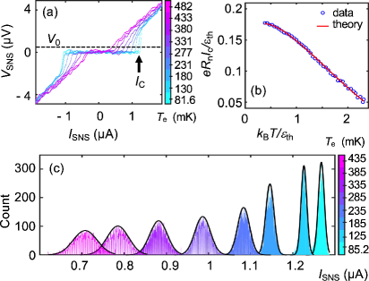
We now move to the description of the electron thermometers. The critical current of an SNS junction is highly sensitive to the electronic temperature in N. The relevant energy scale is the Thouless energy , where is the diffusion constant in N and is the junction length Dubos-PRB01 . For , decreases rapidly with increasing temperature, allowing it to be used as a secondary electron thermometer Meschke-JLTP09 ; WangAPL18 . In a single IV characteristic, the switching current is defined as the value of the current at which the voltage is larger than a threshold voltage chosen above the measurement noise level. Figure 2(a) shows a series of such characteristics at different bath temperatures. Switching current histograms, together with a gaussian fit of their envelope, are shown in Fig. 2(c) for a series of bath temperature values. The histogram width increases with the temperature, consistently with a Josephson energy fluctuating by . In Fig. 2(b), the variation of the critical current with the bath temperature fits nicely the theoretical expectation Dubos-PRB01 , the latter being used as the thermometer calibration. The low Thouless energy 5 eV was chosen in order to avoid a saturation of . The thermometer thus remains sensitive at low temperature, where thermal transport through the gains importance compared to other heat relaxation processes.
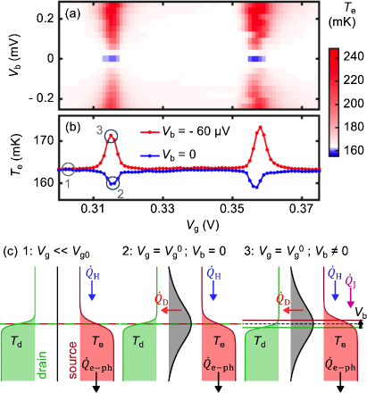
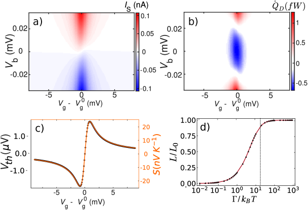
In the experiment, we heat up the source by applying a constant heating power 6 fW to the heater junction. The drain is biased at a potential , the source side being grounded via one of the SNS thermometer contacts. Figure 3(a) shows a map of the source electronic temperature as a function of and . Its resemblance to the charge conductance map of Fig. 1(d) is striking. The source temperature increases rapidly with increasing charge current due to the related Joule power. Right at the charge degeneracy point, the source temperature is lower than in the rest of the map. The higher resolution temperature map of Fig. 4(a) shows a clear cooling region of ellipsoidal shape, with slightly canted axes. This cooling effect is the result of the enhanced heat transfer between the hot source and cold drain.
Figure 3(c) shows energy diagrams for three different cases indicated by circles in the temperature profiles at two different bias of Fig. 3(b). At zero bias and far away from charge degeneracy (case 1), there is neither Joule power nor heat flow through the . The source is overheated up to mK due to the balance between the applied power and the main thermal leakage channel, namely the electron-phonon coupling . Still at zero bias, but near a charge degeneracy point (case 2), there is a heat flow through the , but still no charge flow. This shows up (blue curve in Fig. 3(b)) as a temperature drop by several mK at the charge degeneracy point. The gate-controlled QD junction thus acts as a heat valve. At higher bias (case 3), this cooling contribution is overcome by the Joule heat . A temperature maximum is thus observed at values of the gate potential close to the charge degeneracy point (red curve in Fig. 3(b)).
The mere observation of cooling at the charge degeneracy point is in clear contradiction with the theoretical prediction in the weak coupling, sequential tunneling regime. Indeed the present experiment deals with a strong tunnel coupling between the QD and the leads, with a ratio , rendering the weak coupling picture inapplicable.
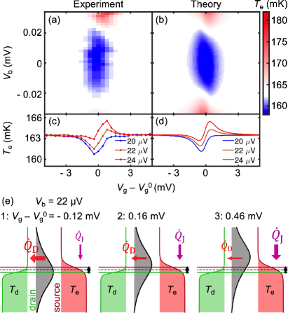
We now go beyond the sequential tunneling approximation. Thanks to the extremely high charging energy, in the vicinity of a charge degeneracy point, the device can be described as a non-interacting single energy level. We are interested in exploring the properties of the leads at stationarity and in particular their electronic temperature; in the NEGFs framework this is possible via the so-called inbedding technique stefleebooka ; Talarico-PRB20 ; suppmat . It is worth mentioning that it is not based on a full heat balance model accounting for the heat flow via phonons and the superconducting leads. We instead assume that the electron-phonon coupling strength itself does not change appreciably within the temperature range of the map, which is equivalent to assume that the main particle and energy redistribution processes in the lead are dominated by electron-electron interactions. By including in the theory the measured temperature (163.5 mK) of the source when decoupled from the , we effectively take into account its thermal coupling to the bath.
The theoretical temperature map around a charge degeneracy point is shown in Fig. 4(b) and reveals a nice agreement with the experimental data in Fig. 4(a). Here, the temperature of the drain is set to 85 mK and the coupling of the QD to the drain is asymmetric with a coupling ratio 3/17 between left and right leads and = 0.25. These best fit values allow us to reproduce semi-quantitatively the temperature profiles of the crossing region, see Fig. 4(c,d). The width in gate potential of the cooling region is independent of the bath temperature and increases with the coupling suppmat . Conversely its extension in bias depends weakly on and increases with the temperature difference across the junction.
The present case actually has some similarities with the regime of a metallic Single Electron Transistor where cooling at the charge degeneracy point was also found Kubala-PRL08 ; Dutta-Nanolett19 . Nevertheless, an asymmetry in gate voltage is clearly observed in the experimental and theoretical temperature map. For a bias voltage around 22 , the source temperature can be tuned either below or above the reference temperature of 163.5 mK by acting on the gate voltage, see Fig. 4(c). This behavior is not to be expected in the case of a metallic island where electron-hole symmetry in the density of states makes transport properties symmetric across the charge degeneracy point. Therefore it is an unambiguous signature of the QD discrete energy spectrum. At a given bias, the value of the gate potential determines the position of the broadened energy level in the QD (see the grey profile in Fig. 4(e)) and thus the mean energy of the tunneling electrons. This in turn affects the heat balance in the source and modifies the boundary of the cooling region in the temperature map. The extension in bias of this crossover zone, where one can switch from cooling to heating by adjusting with the gate, depends on both the coupling and the temperature difference across the QD suppmat .
This work shows that electronic heat transport through a QD junction can be modulated by a gate potential, making it act as a gate-tunable heat valve. This behavior can have important consequences in the practical thermo-electric efficiency of such a single quantum-dot junction Harzheim-PRR20 . The Coulomb diamond patterns in the temperature maps reveal the intimate relation between charge conductance on one hand and heat transport and dissipation on the other. Further experiments may allow a quantitative comparison of thermal effects to the charge transport properties, in a wide range of tunnel couplings. The ability of precision electron thermometry at the heart of a QD-based device demonstrated here opens wide perspectives in the field of heat transport and dissipation in quantum electronic devices, paving the way for quantitative tests of the Landauer principle in the quantum information regime RevuePekola .
Acknowledgements.
The authors thank B. Karimi and J. P. Pekola for stimulating discussions. Samples were realized at the Nanofab platform at Institut Néel with the help of T. Crozes. We acknowledge support from the Nanosciences Foundation under the auspices of the Foundation UGA and from the European Union under the Marie Skłodowska-Curie Grant Agreement 766025. NLG and WNT acknowledge support from the Academy of Finland Center of Excellence program (Project no. 312058) and the Academy of Finland (Project no. 287750). NLG acknowledges funding from the Maupertuis Program for a RSM grant and from the Turku Collegium for Science and Medicine. Numerical simulations were performed at the Finnish CSC facilities under the Project no. 2000962.References
- (1) E. Pop, ”Energy dissipation and transport in nanoscale devices”, Nano Research 3, 147 (2010).
- (2) W. Lee, K. Kim, W. Jeong, L. Zotti, F. Pauly, J. C. Cuevas, P. Reddy, ”Heat dissipation in atomic-scale junctions”, Nature 498, 209 (2013).
- (3) L. Zotti, M. Bürkle, F. Pauly, W. Lee, K. Kim, W. Jeong, Y. Asai, P. Reddy, J. C. Cuevas, ”Heat dissipation and its relation to thermopower in single-molecule junctions”, New J. Phys. 16, 015004 (2014).
- (4) Y. Dubi and M. Di Ventra, ”Heat flow and thermoelectricity in atomic and molecular junctions”, Rev. Mod. Phys. 83, 131 (2011).
- (5) L. P. Kouwenhoven, D. G. Austing, S. Tarucha, ”Few-electron quantum dots”, Rep. Prog. Phys. 64, 701 (2001).
- (6) R. Scheibner, H. Buhmann, D. Reuter, M. N. Kiselev, and L. W. Molenkamp, ”Thermopower of a Kondo Spin-Correlated Quantum Dot”, Phys. Rev. Lett. 95, 176602 (2005)
- (7) S. F. Godijn, S. Möller, H. Buhmann, and L. W. Molenkamp, S. A. van Langen, ”Thermopower of a Chaotic Quantum Dot, Phys. Rev. Lett. 82, 2927 (1999).
- (8) A. S. Dzurak, C. G. Smith, C. H. W. Barnes, M. Pepper, L. Martĩn-Moreno, C. T. Liang, D. A. Ritchie, and G. A. C. Jones, ”Thermoelectric signature of the excitation spectrum of a quantum dot”, Phys. Rev. B 55, R10197 (1997).
- (9) M. Josefsson, A. Svilans, A. M. Burke, E. A. Hoffmann, S. Fahlvik, C. Thelander, M. Leijnse, H. Linke, ”A quantum-dot heat engine operating close to the thermodynamic efficiency limits”, Nature Nanotech. 13, 1 (2018).
- (10) G. Jaliel, R. K. Puddy, R. Sanchez, A. N. Jordan, B. Sothmann, I. Farrer, J. P. Griffiths, D. A. Ritchie, and C. G. Smith, ”Experimental Realization of a Quantum Dot Energy Harvester”, Phys. Rev. Lett. 123, 117701 (2019).
- (11) D. Prete, P. A. Erdman, V. Demontis, V. Zannier, D. Ercolani, L. Sorba, F. Beltram, F. Rossella, F. Taddei, S. Roddaro, ”Thermoelectric Conversion at 30 K in InAs/InP Nanowire Quantum Dots”, Nano Lett. 19, 3033 (2019).
- (12) P. Kim, L. Shi, A. Majumdar, and P. L. McEuen, ”Thermal transport measurements of individual multiwalled nanotubes”, Phys. Rev. Lett. 87, 215502 (2001).
- (13) Z. Huang, F. Chen, R. D’Agosta, P. A. Bennett, M. Di Ventra, and N. Tao, ”Local ionic and electron heating in single-molecule junctions”, Nature Nanotech. 2, 698 (2007).
- (14) M. Tsutsui, M. Taniguchi, and T. Kawai, ”Local Heating in Metal–Molecule–Metal Junctions”, Nano Lett. 8, 3293 (2008).
- (15) D. Halbertal, J. Cuppens, M. Ben Shalom, L. Embon, N. Shadmi, Y. Anahory, H. R. Naren, J. Sarkar, A. Uri, Y. Ronen, Y. Myasoedov, L. S. Levitov, E. Joselevich, A. K. Geim and E. Zeldov, ”Nanoscale thermal imaging of dissipation in quantum systems”, Nature 539, 407 (2016).
- (16) A. Marguerite, J. Birkbeck, A. Aharon-Steinberg, D. Halbertal, K. Bagani, I. Marcus, Y. Myasoedov, A. K. Geim, D. J. Perello, and E. Zeldov, ”Imaging work and dissipation in the quantum Hall state in graphene”, Nature 575, 628 (2019).
- (17) L. W. Molenkamp, Th. Gravier, H. van Houten, O. J. A. Buijk, M. A. A. Mabesoone, and C. T. Foxon, ”Peltier coefficient and thermal conductance of a quantum point contact”, Phys. Rev. Lett. 68, 3765 (1992).
- (18) J. R. Prance, C. G. Smith, J. P. Griffiths, S. J. Chorley, D. Anderson, G. A. C. Jones, I. Farrer, and D. A. Ritchie, ”Electronic Refrigeration of a Two-Dimensional Electron Gas”, Phys. Rev. Lett. 102, 146602 (2009).
- (19) S. Jézouin, F. D. Parmentier, A. Anthore, U. Gennser, A. Cavanna, Y. Jin, and F. Pierre, ”Quantum Limit of Heat Flow Across a Single Electronic Channel”, Science 342, 601 (2013).
- (20) E. Sivre, A. Anthore, F. D. Parmentier, A. Cavanna, U. Gennser, A. Ouerghi, Y. Jin, and F. Pierre, ”Heat Coulomb blockade of one ballistic channel”, Nature Phys. 14, 145 (2018).
- (21) M. Banerjee, M. Heiblum, V. Umansky, D. E. Feldman, Y. Oreg, and A. Stern, ”Observation of half-integer thermal Hall conductance”, Nature 559, 205 (2018) .
- (22) E. S. Tikhonov, D V Shovkun, D Ercolani, F Rossella, M Rocci, L Sorba, S Roddaro and V S Khrapai, ”Noise thermometry applied to thermoelectric measurements in InAs nanowires”, Semicond. Sci. Technol. 31, 104001 (2016).
- (23) M. Nahum and J. M. Martinis, ”Ultrasensitive hot electron microbolometer”, Appl. Phys. Lett. 63, 3075 (1993).
- (24) F. Giazotto, T. T. Heikkilä, A. Luukanen, A. M. Savin and J. P. Pekola, ”Opportunities for mesoscopics in thermometry and refrigeration: Physics and applications”, Rev. Mod. Phys. 78, 217 (2006).
- (25) M. Meschke, J. T. Peltonen, H. Courtois, J. P. Pekola, ”Calorimetric Readout of a Superconducting Proximity-Effect Thermometer”, J. Low Temp. Phys. 154, 190 (2009).
- (26) L. B. Wang, O. P. Saira, J.-P. Pekola, ”Fast thermometry with a proximity Josephson junction”, Appl. Phys. Lett.112, 013105 (2018).
- (27) F. Giazotto, and M. J. Martĩnez-Perez, ”The Josephson heat interferometer”, Nature 492, 41 (2012).
- (28) A. Ronzani, B. Karimi, J. Senior, C. Chen, and J. P. Pekola, ”Tunable photonic heat transport in a quantum heat valve”, Nature Phys. 114, 991 (2018).
- (29) O. P. Saira, M. Meschke, F. Giazotto, A. M. Savin, M. Möttönen, J. P. Pekola, ”Heat transistor: demonstration of gate-controlled electronic refrigeration”, Phys. Rev. Lett. 99, 027203 (2007).
- (30) B. Dutta, J. T. Peltonen, D. S. Antonenko, M. Meschke, M. A. Skvortsov, B. Kubala, J. König, C. B. Winkelmann, H. Courtois, and J. P. Pekola, ”Thermal Conductance of a Single-Electron Transistor”, Phys. Rev. Lett. 119, 077701 (2017).
- (31) B. Kubala, J. König, and J. Pekola, ”Violation of the Wiedemann-Franz Law in a Single-Electron Transistor”, Phys. Rev. Lett. 100, 066801 (2008).
- (32) H. L. Edwards, Q. Niu, A. L. de Lozanne, ”A quantum dot refrigerator”, Appl. Phys. Lett. 63, 1815 (1993).
- (33) B. Dutta, D. Majidi, A. Garcia Corral, P. A. Erdman, S. Florens, T. A. Costi, H. Courtois, C. B. Winkelmann, ”Direct probe of the Seebeck coefficient in a Kondo-correlated single-quantum-dot transistor”, Nano Letters 19, 506 (2019).
- (34) T. Kontos, M. Aprili, J. Lesueur, X. Grison, and L. Dumoulin, ”Superconducting Proximity Effect at the Paramagnetic-Ferromagnetic Transition”, Phys. Rev. Lett. 93, 137001 (2004).
- (35) H. Park, A. K. Lim, A. P. Alivisatos, J. Park, and P. L. McEuen, ”Fabrication of metallic electrodes with nanometer separation by electromigration”, Appl. Phys. Lett. 75, 301 (1999).
- (36) Here we use the definition where is the total capacitance of the dot with respect to leads and gate.
- (37) See Supplemental Material, which includes Refs. [38-43].
- (38) K. I. Bolotin, F. Kuemmeth, A. N. Pasupathy, and D. C. Ralph, ”Metal-nanoparticle single-electron transistors fabricated using electromigration”, Appl. Phys. Lett. 84, 3154 (2004).
- (39) D. C. Ralph, C. T. Black, and M. Tinkham, ”Spectroscopic Measurements of Discrete Electronic States in Single Metal Particles”, Phys. Rev. Lett. 74, 3241 (1995).
- (40) D. M. T. van Zanten, F. Balestro, H. Courtois, and C. B. Winkelmann, ”Probing hybridization of a single energy level coupled to superconducting leads”, Phys. Rev B 92, 184501 (2015).
- (41) J. M. Thijssen and H. S. J. van der Zant, ”Charge transport and single-electron effects in nanoscale systems”, Phys. Stat. Sol. (b) 245, 1455 (2008)
- (42) E. Bonet, M. M. Deshmukh, and D. C. Ralph, ”Solving rate equations for electron tunneling via discrete quantum states”, Phys. Rev. B 65, 045317 (2002).
- (43) J. T. Peltonen, P. Virtanen, M. Meschke, J. V. Koski, T. T. Heikkilä, J. P. Pekola, ”Thermal conductance by the inverse proximity effect in a superconductor”, Phys. Rev. Lett. 105, 097004 (2010).
- (44) P. Dubos, H. Courtois, B. Pannetier, F. K. Wilhelm, A. D. Zaikin, and G. Schön, ”Josephson critical current in a long mesoscopic S-N-S junction”, Phys. Rev. B 63, 064502 (2001).
- (45) G. Stefanucci and R. van Leeuwen, ”Nonequilibrium many-body theory of quantum systems”, Cambridge University Press, Cambridge, UK, 2013.
- (46) N. W. Talarico, S. Maniscalco, N. Lo Gullo, ”Study of the energy variation in many-body open quantum systems: Role of interactions in the weak and strong coupling regimes”, Phys. Rev. B 101, 045103 (2020).
- (47) A. Harzheim, J. K. Sowa, J. L. Swett, G. A. D. Briggs, J. A. Mol, and P. Gehring, ”Role of metallic leads and electronic degeneracies in thermoelectric power generation in quantum dots”, Phys. Rev. Res. 2, 013140 (2020).
- (48) J. P. Pekola, ”Towards quantum thermodynamics in electronic circuits”, Nature Physics 11, 118 (2015).
Supplemental Material: A Single-Quantum-Dot Heat Valve
Supplemental Material: A Single-Quantum-Dot Heat Valve
B. Dutta D. Majidi N. W. Talarico N. Lo Gullo C. B. Winkelmann H. Courtois
In this supplemental material part, we discuss about the sample fabrication, charge transport properties, performance of our thermometer junction as a bolometric detector, and the details of the theoretical approach used to explain our data.
I Sample fabrication and charge transport characteristics
We have used a Si substrate covered with a 300 nm SiO2 oxide, from which gold films thinner than about 10 nm are known to dewet. Yet, and most interestingly, the gold nanoparticles even happen to form on top of the noble metal surfaces (Au, Pt) from which the electromigration constriction is formed. This means that a thin gold film does not wet on gold. This was also observed by the Cornell group Bolotin2004 . In line with these authors, we believe that even after thorough pumping down to a few mbar (as is usual in evaporation chambers), the noble metal surfaces are still not clear of a contaminant layer (e.g. water), which leads to dewetting of the nm-thin gold top layer.
The samples in Ref. Dutta-Nanolett19 and in the present manuscript share the same geometry and fabrication technique but they are different samples that were fabricated in two different runs. The formation of a nano-gap by electromigration depends sensitively of the structural details (precise width and thickness) of the constriction, therefore the size of the gap (between leads and dot) and its structural details vary from one electromigration to other. As a result, the strength of tunnel coupling also varies. Here, the tunnel coupling in Ref. Dutta-Nanolett19 device was about 10 times larger than in the present device. In both cases Pt was used as the electro-migration material, as it suppresses the superconducting proximity effect extremely efficiently, much more than Au.
The charging energy of the dot depends on the actual size of the Au nano-island and the total effective capacitance with its environment, that is determined by both the precise nature of the evaporated Au droplets and the detailed structure of the nano-gap created by electromigration. Therefore, it is expected to have a different charging energy for two otherwise similar samples. Metallic quantum dots have been investigated in the 90s. In Ref. Ralph-PRL95 , an energy level separation of 0.7 meV and a charging energy of 6 meV were deduced from the measured energy spectra in 10 nm Al nanoparticles. The nanoparticles used in our work can be seen from SEM images to be about 5 nm in size and we expect an energy level separation of the order of a few meV. In a previous work vanZanten-PRB16 from our group, the weak coupling to leads enabled us to observe sharp resonances in the differential conductance map corresponding to an energy level separation of about 5 meV.
Figure 1 of the main text displays the differential conductance map as a function of both the bias and gate voltages and respectively. A Coulomb diamond pattern is clearly, but partly, visible. The charging energy of 4 meV is estimated from extrapolating the bias at the top of a diamond, which is actually twice the charging energy Thijssen-PSSB08 . We did not measure this device above bias voltages of about 4 mV, as, due to the rather large tunnel couplings, this voltage leads to currents of about 6 nA, beyond which we observe instabilities related to inelastic processes. At higher bias, there is a risk of burning the device. Therefore, a full spectroscopic characterization revealing several successive levels was not possible.
The detailed shape of the Coulomb diamond pattern can be used to determine the different capacitive couplings of the QD to its environment. In particular the sum of the inverse of the diamond (positive and negative) slopes is equal to the ratio of the total capacitance to its leads over the capacitance to the gate Bonet-2002 . The so-called coupling parameter translates the effect of the gate voltage in terms of shift in chemical potential of the QD. Here we obtain 0.157.
We now discuss the nature of charge transport through the QD. This can be done by means of the differential conductance data shown in Fig. 1 (d) of the main text. In Fig. S1 we show the measured differential conductance (left) and the corresponding current (right) obtained by integrating it, both at the charge degeneracy point .
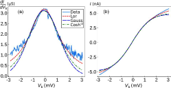
We first compare the measured differential conductance to the theoretical expression for the charge transport through a single quantum level:
| (S1) |
where is the Fermi-Dirac distribution. The total broadening is given by where is induced by the coupling to the leads whereas is added to account for a possible extra broadening mechanism such as fluctuations of the applied gate voltage. For now we assume . Around the resonance , the differential conductance has a Lorentzian shape with a width given by and a maximum determined by the ratio . Figure S1(a) shows, in parallel with the experimental data, the best fit with the two free fit parameters and . The agreement is excellent. Here the temperature of both leads set to does not contribute significantly to the obtained lineshape. In addition, Fig. S1 includes alternative fits with a Gaussian or a profile for the differential conductance. These fits are much less in accordance with the data, which strengthens the above conclusion.
The above analysis demonstrates that electron transport occurs through a single-level quantum dot. The observed Lorentzian line-shape is a strong indication that the main mechanism for the broadening of the spectral function of the dot is due to the coupling with the leads. Any other mechanism, if present, contributes only marginally.
II Performance of a SNS junction as a bolometer
In order to measure the heat flow through a QD junction, which is described in the main text, one needs to be able to access a very small change in electronic temperature. Moreover, one needs an operating temperature of down to 100 mK or below, where the QD heat flow dominates over the other paths of heat relaxation such as electron-phonon coupling. These two requirements lead us to consider SNS proximity junction as a thermometer that can fulfill both of these requirements. We have optimized the sensitivity of the SNS thermometer with several repetitions of the junctions parameters such as the length and thickness of the normal metal. In this way, we reduced the Thouless energy () of the SNS junction, which basically determines the lowest saturation temperature of the thermometer Dubos-PRB01b .
Here we describe a test experiment, where we determine the sensitivity of our optimized SNS thermometer and test its operation as a bolometric detector. The SEM image of the device under test is shown in Fig. S2(a), where the normal metal Au is shown in red color and the superconducting Al leads in light-blue. The basic structure of the device is similar to that of the QD device described in the main text, with the only difference that there is no QD is placed in between source and drain after the electromigration. Therefore, the device can be essentially considered as a 5 m long and 100 nm wide rectangular normal metallic island. Like the samples discussed in the main text it has a very long SNS junction to inject Joule heat into it and a short SNS junction to measure the electronic temperature.
We heat-up the island by applying a constant adjustable d.c. current through the heater junction, using a 1.3 V isolated d.c. battery. The SNS thermometer is calibrated against the well known bath temperature, by measuring the histograms of its stochastic switching current, as described in the main text. Here we present an experiment, where the bath temperature is at = 90 mK and the heater junction is current-biased through a 200 M biasing resistor, which leads to a heating power = 100 aW. We continuously monitor the electronic temperature of the island by measuring a histogram of 500 switching currents in about 1 sec. The real time temperature trace of the island is shown in Fig. S3. One can easily identify the change of the electronic temperature by a few mK w.r.t. the background temperature of about 92 mK, whenever the heater is turned on (off). Therefore the thermometer clearly detects an input heat as low as 100 aW, thus performing as a bolometric detector of very small heating power. The noise equivalent power is about 100 aW/.

This observation of the island’s electronic temperature can be determined by a heat-balance equation, as shown by a heat-balance model in the Fig. S2(b):
| (S2) |
where is the material dependent constant, is the volume of the island, and are the electron and the bath (phonon) temperatures respectively. Any parasitic heat source (sink) such as heat losses through the superconducting leads due to imperfect thermal insulation Joonas-PRL2010 or parasitic heating by the electromagnetic environment are taken into account within the injected heating power .
The electronic temperature of the island can be extracted by solving the above heat-balance equation (S2). If we use an injected heating power = 100 aW, the material constant for Au Wm-3K-5 Giazotto-RMP06 , the volume of the island m3 and the bath temperature 80 mK, we get an increase of the electronic temperature 3 mK, which is consistent with the measured value. This justifies the analysis of the heat relaxation mechanism in the island as discussed above.
In the experiment described in the main text, we use a saw-tooth shaped a.c. current bias of the junction to measure 3000 switching events in about 10 sec. The critical current of the junction is determined as the gaussian maximum. The thermometer sensitivity is found to be 1.5 A/K at 80 mK, with a noise level of about 200 K/.
III Inbedding technique
Here, we give a brief overview of the inbedding technique used to compute the non-equilibrium steady-state of the leads and their electronic temperatures under the hot-electron assumption. The Hamiltonian of the total system (quantum dot plus source and drain reservoirs) is given by:
| (S3) | |||||
| (S4) | |||||
| (S5) |
where is the gate voltage measured from the considered resonance and accounting for the coupling parameter. the coupling Hamiltonian between the quantum dot, , and the leads. Using the non-equilibrium Green’s function approach stefleebook , and assuming that the whole system reaches a (possibly non-equilibrium) stationary state, the state of the is completely characterized by the retarded and lesser single-particle Green’s functions:
| (S6) | |||||
| (S7) |
here is the advanced component of the Green’s functions. is the Fourier transform of the retarded Green’s function of the isolated (non-coupled to the leads) quantum dot , with . The embedding self-energy is defined as , with and the Fourier transform of isolated leads’ Green’s functions. We work in the wide band limit approximation (WBLA) and therefore we have: . The first equation in Eqs. S6 is the Dyson equation for the retarded component of the single-particle Green’s function, from which the spectral function of the can be computed as .
The embedding self-energy approach accounts for the effect that the leads have on the physical properties of the system, but once the solution to Eqs. S6 are obtained, it is possible to find the Green’s functions of the leads and explore the influence of the on the physical features of the reservoirs. By introducing the inbedding self-energy one has the following relations:
| (S8) | |||
| (S9) | |||
The lesser Green’s functions of the leads are different from the isolated ones , with the Fermi-Dirac distributions characterized by the initial chemical-potential and temperature and . From the knowledge of we can compute both the average particle number and energy of the leads: and .
We now resort to the hot electron assumption that accounts for a neat separation of the energy relaxation time scales between system and leads. Basically, it assumes that the electron-electron interactions into the leads makes their equilibration time much faster than any other dynamical processes in the whole system. Therefore, we can assume that the leads at the steady state are described by a new Fermi-Dirac distribution with a different set of chemical potential and temperature and . The two parameters are the solution of the set of non-linear equations:
| (S10) | |||
| (S11) |
IV Particle and energy currents
Within the non-equilibrium Green’s function formalism, particle, energy and heat currents of the source lead are given by the following expressions:
| (S12) | |||
| (S13) | |||
| (S14) |
where we used the definition of the transmission coefficient in the WBLA which is valid beyond the single level approximation for the dot. For the set of parameters considered in the main text, the heat and particle currents for the source are shown in Fig. S4. It is interesting to notice the resemblance between the heat current map and the temperature map shown in the main text. It confirms that in the regime we explored the temperature changes in the source lead correspond indeed to a heat current to/from the source (panel (a) in Fig. S4). At large bias the source heats up; the system behaves as a heater, namely the energy of the bias is transformed into internal energy. At low bias we observe instead heat flow from the hot to the cold lead; the system behaves as a valve, meaning that it enables the natural flow of heat from the hot to the cold lead. It is also interesting to observe that there is a whole region in which heat and particle currents have opposite signs.
It is worth to mention that this effect is not due to the onset of a thermovoltage which would make particles flow against the applied bias voltage without necessarily causing an inversion of heat current. The thermovoltage, although present, is very small compared to the extension in bias voltage where the mismatch in sign is observed. This is shown in Fig. S4 panel (c) where we plot the thermovoltage , together with the corresponding thermopower, defined as the bias voltage at which the particle current vanishes.
The observed significant thermal conductance is a signature of the strong coupling of the QD to the leads. We computed the Lorentz ratio where and are the thermal and electrical conductivities respectively. In panel (d) of Fig. S4 we plot the Lorentz number with at the charge degeneracy point . The dashed line corresponds to the ratio considered in the system presented in the main text. It is clear that the deviation from the WF law is small because of the strong coupling to the leads.
V The cooling and transition regions
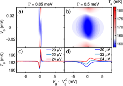
Figure S5 shows the map of the calculated electronic temperature for couplings (panels (a) and (c)) and (panels (b) and (d)) and for the same drain temperature at closed gate voltage mK similarly to Fig. 3 of the main text. A change in the coupling changes the extension of the cooling region in the gate voltage but it does not affect dramatically the extension of the cooling region in the bias voltage nor the position of the transition from cooling to heating. Compared to the discussion in the main text and in Figure S5, we consider a symmetric coupling of the dot to the leads, which increases the amplitude of the cooling.
To give a more quantitative analysis we computed the extension of the cooling region in the bias voltage at and its width in gate voltage for different couplings and temperatures of the drain at closed gate. The results are plotted in Fig. S6 in panels (a) and (b) where it can be appreciated that the coupling constant does not change significantly the extension in bias which instead strongly depends upon the difference in the equilibrium temperatures between the drain and source. Indeed as the temperature of the drain increases towards the temperature of the source the extension in shrinks. Nevertheless the extension in the gate voltage is only determined by the coupling and does not present any significant dependence upon the closed gate temperature of the drain.
The transition region, namely the region where at fixed bias it is possible to obtain both heating and cooling by changing the gate potential, has a strong dependence on both the coupling and the temperature difference at closed gate. This is shown in Fig. S6 panels (c) and (d) where we plot the width and extension of the transition region; they have been determined by finding the curve such that 163.5 mK and then taking whereas is the difference between the voltage gates at which is larger than its values at closed gate plus on both sides. It can be observed that this region becomes smaller as the coupling is increased whereas its width increases with the coupling. The width also decreases steadily as the temperature of the drain increases whereas the behavior of its width with temperature is less trivial. It decreases at large couplings whereas it increases as the temperature increases at small couplings.
VI Couplings to the leads and single-level nature of the dot
Here we want to show how we proceeded to determine the magnitude of the tunnel coupling of the QD to the source and the drain, namely and . Moreover we will also show how we assessed the single-level nature ruling out the possibility of the presence of more levels. From the microscopic point of view, the coupling depends on the wave-functions of the level considered as well as the density of state of the leads at that energy. For this reason it can vary appreciably for different resonances. Here we focus on the resonance chosen in the main text to describe the heat valve effect as this is the focus of our work. By comparing the heat flowing into the source lead shown in Fig. S5 panel b) with the temperature maps in Figure 4 of the main text, we see that the cooling region corresponds to the region where heat flows away from the source. Therefore there is a strict connection between the cooling region in the temperature map and the region where the heat flow is negative.
From Equation S14, and assuming for now a single-level at energy , the heat current is given by:
| (S15) |
where is the Fermi-Dirac distribution, is the total coupling to the leads and is the asymmetry in the coupling. The total broadening given by includes some extra contribution which accounts for extra broadening mechanisms such as fluctuations of the applied gate voltage. The above expression tells us that the total broadening is responsible for the width of the curve whereas the height of the same curve is determined by both the total coupling and the asymmetry . It is easy to check that, at fixed and the maximum heat current is achieved at . We have seen in the previous section that the width of the cooling region at depends crucially only on the total width , namely the width of the spectral function of the quantum dot.
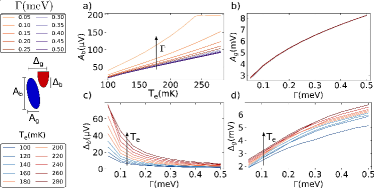
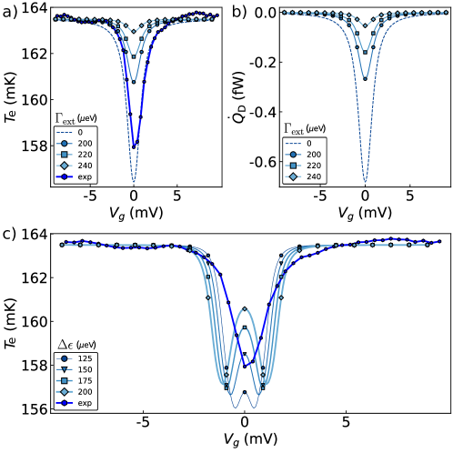
Let us now assume that the broadening observed in the temperature map in Fig. 4 of the main text is mostly due to some external source therefore having . In this case the total heat current would be greatly reduced. In Fig. S7 panel a) we compare the temperature profile as a function of the gate voltage at zero bias for (dashed) the theoretical calculation used in Fig. 4 of the main text and (thin solid lines with markers) the case of , and different such that . We have also added the experimentally measured temperature profile (thick solid line). In panel b) of Fig. S7 we plot the corresponding heat currents. We can see that if the broadening would be due mostly to some other mechanism other than the coupling to the leads, even in the best case scenario of symmetric coupling () where the cooling power is maximum, we would not reach the current needed for the observed cooling. We therefore conclude that the main mechanism for the broadening of the spectral function is due to the coupling to the leads.
The asymmetry parameter used in Fig. 4 of the main text has been chosen in order to get the best match between the observed temperature profiles and the computed ones with the inbedding technique. We therefore conclude that the resonance used in heat valve effect discussed in the main text is strongly coupled to the leads. Furthermore we have shown that any other broadening mechanism, if present at all, does not contribute substantially to the width of the spectral function of the level.
We now move to the discussion of the single-level nature of the QD. Figure S7 panel c) shows the theoretical prediction for the temperature variation as a function of the gate voltage for the case of two levels and compares it with the single-level prediction and the experimental data. We have used as established above and we have set the ratio for the two-level case too. The separation between the two levels has been chosen to be in order to make them distinguishable from a single degenerate level but such that the two levels are not completely separated. In this latter case their effect would be the same as that of two single-level resonances. It is clear from this comparison that if more than one level is involved the temperature profile at zero bias would be markedly different. We therefore conclude that the measured temperature profile is indeed consistent with a strongly coupled single level, which is consistent with the charge transport data.
References
- (1) K. I. Bolotin, F. Kuemmeth, A. N. Pasupathy, and D. C. Ralph, ”Metal-nanoparticle single-electron transistors fabricated using electromigration”, Appl. Phys. Lett. 84, 3154 (2004).
- (2) B. Dutta, D. Majidi, A. Garcia Corral, P. A. Erdman, S. Florens, T. A. Costi, H. Courtois, C. B. Winkelmann, ”Direct probe of the Seebeck coefficient in a Kondo-correlated single-quantum-dot transistor”, Nano Letters 19, 506 (2019).
- (3) D. C. Ralph, C. T. Black, and M. Tinkham, ”Spectroscopic Measurements of Discrete Electronic States in Single Metal Particles”, Phys. Rev. Lett. 74, 3241 (1995).
- (4) D. M. T. van Zanten, F. Balestro, H. Courtois, and C. B. Winkelmann, ”Probing hybridization of a single energy level coupled to superconducting leads”, Phys. Rev B 92, 184501 (2015).
- (5) J. M. Thijssen and H. S. J. van der Zant, ”Charge transport and single-electron effects in nanoscale systems”, Phys. Stat. Sol. (b) 245, 1455 (2008)
- (6) E. Bonet, M. M. Deshmukh, and D. C. Ralph, ”Solving rate equations for electron tunneling via discrete quantum states”, Phys. Rev. B 65, 045317 (2002).
- (7) P. Dubos, H. Courtois, B. Pannetier, F. K. Wilhelm, A. D. Zaikin, and G. Schön, ”Josephson critical current in a long mesoscopic S-N-S junction”, Phys. Rev. B 63, 064502 (2001).
- (8) J. T. Peltonen, P. Virtanen, M. Meschke, J. V. Koski, T. T. Heikkilä, J. P. Pekola, ”Thermal conductance by the inverse proximity effect in a superconductor”, Phys. Rev. Lett. 105, 097004 (2010).
- (9) F. Giazotto, T. T. Heikkilä, A. Luukanen, A. M. Savin and J. P. Pekola, ”Opportunities for mesoscopics in thermometry and refrigeration: Physics and applications”, Rev. Mod. Phys. 78, 217 (2006).
- (10) G. Stefanucci and R. van Leeuwen, ”Nonequilibrium many-body theory of quantum systems”, Cambridge University Press, Cambridge, UK, 2013.