Tunable nanophotonics enabled by chalcogenide phase-change materials
Abstract
Nanophotonics has garnered intensive attention due to its unique capabilities in molding the flow of light in the subwavelength regime. Metasurfaces (MSs) and photonic integrated circuits (PICs) enable the realization of mass-producible, cost-effective, and highly efficient flat optical components for imaging, sensing, and communications. In order to enable nanophotonics with multi-purpose functionalities, chalcogenide phase-change materials (PCMs) have been introduced as a promising platform for tunable and reconfigurable nanophotonic frameworks. Integration of non-volatile chalcogenide PCMs with unique properties such as drastic optical contrasts, fast switching speeds, and long-term stability grants substantial reconfiguration to the more conventional static nanophotonic platforms. In this review, we discuss state-of-the-art developments as well as emerging trends in tunable MSs and PICs using chalcogenide PCMs. We outline the unique material properties, structural transformation, electro-optic, and thermo-optic effects of well-established classes of chalcogenide PCMs. The emerging deep learning-based approaches for the optimization of reconfigurable MSs and the analysis of light-matter interactions are also discussed. The review is concluded by discussing existing challenges in the realization of adjustable nanophotonics and a perspective on the possible developments in this promising area.
I Introduction
In recent years, an ever-increasing competition has arisen between two exciting technologies, i.e., electronics and photonics, to realize ubiquitous functionalities from imaging and communication to sensing and medicine Sun et al. (2015); Atabaki et al. (2018); Zeng et al. (2014). Despite the striking progress of electronics in data processing and storage as well as logic operations, photonic platforms are preferred for information transportation, mostly because of the higher speed and larger bandwidth Rickman (2014); Thomson et al. (2016); Genevet et al. (2017). However, to beat the fingerprints of electronics, i.e., integrability and reprogrammability, photonics needs to evolve into the next generation of miniaturized systems incorporating reconfigurable platforms with adjustable properties to fully manipulate the key features of photons, the information carrier in photonic platforms.
Metasurfaces (MSs) and photonics integrated circuits (PICs) are currently the two mature nanophotonics platforms the manipulation of light for on-chip and free-space applications, respectively. MSs, the two-dimensional analog of metamaterials, have attracted significant attention due to their unprecedented ability to control incident electromagnetic fields in the subwavelength regime Yu et al. (2011); Staude et al. (2013); Arbabi et al. (2015). Owing to their judiciously engineered optical scatterers, or the so-called meta-atoms, arranged in a periodic or aperiodic texture, the amplitude, phase, polarization, and frequency of the impinging light can be spatially and spectrally manipulated, making a big step towards the realization of the next-generation flat optics Khorasaninejad et al. (2016); Ding et al. (2018a); Yesilkoy et al. (2019). A myriad of novel phenomena and optical functionalities have thus been demonstrated including beam shaping and steering Arbabi et al. (2016), polarization generation Arbabi et al. (2018a), large-angle holography Lee et al. (2018), directional lasing Ha et al. (2018), analog computing Abdollahramezani et al. (2017), quantum emission Tran et al. (2017), nonlinear generation Krasnok et al. (2018a), structural coloration Hemmatyar et al. (2019), and biosensing Krasnok et al. (2018b). Similarly, complementary metal-oxide semiconductor (CMOS)-compatible silicon (Si) and silicon nitride (SiN) PICs have experienced phenomenal transformations over the past decade. Several key infrastructures such as modulators, (de)multiplexers, filters, and detectors featuring low optical attenuation, high optical mode confinement, wide operational bandwidth from visible (vis) to beyond infrared (IR), and immunity to electromagnetic interference have enabled a wave of ubiquitous applications including data communication, spectroscopy, and sensing.
However, the main challenge with the developed static MS configurations is that their assigned functionality remains fixed once fabricated, hindering many practical free-space applications that need real-time tuning Jahani and Jacob (2016); Kuznetsov et al. (2016); Baranov et al. (2017); Staude and Schilling (2017); Ding et al. (2017); Su et al. (2018); Ding et al. (2018b); Kamali et al. (2018); Neshev and Aharonovich (2018); Tseng et al. (2018); Luo (2018); He et al. (2018); Wen et al. (2018a); Chen et al. (2019); Zang et al. (2019); Staude et al. (2019); Sung et al. ; Vaskin et al. (2019); Chen et al. ; Koshelev et al. ; Fan et al. (2019a). On the other hand, most on-chip photonic demonstrations are based on the application-specific designs of PICs. To orient the potential of PICs for emerging applications of microwave photonics, neuromorphic computing, and quantum computation, high reconfigurable and general-purpose platforms similar to the field-programmable gate array (FPGA) in electronics are indispensable Zhuang et al. (2015); Capmany et al. (2016); Harris et al. (2017); Pérez et al. (2017); Shen et al. (2017); Tait et al. (2017); Wang et al. (2018); Kim et al. (2019).
There exist several approaches in which external stimuli such as electrical current, electrostatic fields, heat, chemical reactions, mechanical forces, magnetic fields, and optical pumping are applied to adapt the functionality of MSs dynamically. Such approaches rely on the incorporation of two-dimensional (2D) materials (including graphene and transition-metal dichalcogenides) Sherrott et al. (2017), highly doped semiconductors [such as Si and germanium (Ge)] Lewi et al. (2015), transparent conductive oxides (such as indium tin oxide) Kafaie Shirmanesh et al. (2018), phase-transition materials (such as vanadium dioxide) Kim et al. , metal hydrides (such as hydrogenated palladium and magnesium) Palm et al. (2018), liquid crystals Komar et al. (2017), micro-electromechanical devices Arbabi et al. (2018b), elastic platforms Kamali et al. (2016), and plasmonic‐metal/semiconductor heterostructures Zuev et al. (2016); Taghinejad et al. (2018); Lepeshov et al. (2019a) with nanophotonics frameworks. On the other hand, PICs primarily rely on intrinsic thermo-optics and electro-optics effects of the Si and SiN to enable reconfigurable building blocks. However, the modest range of these properties has spurred the development of hybrid integrated platforms employing secondary materials including electro-optics polymers (such as organic polymers) Koos et al. (2009), 2D materials (such as graphene) Phare et al. (2015), phase-transition materials Markov et al. (2015), noble metals (such as Au) Haffner et al. (2015), and semiconductors (such as germanium) Feng et al. (2012).
Amongst existing approaches, the integration of phase-change materials (PCMs), specially chalcogenide alloys, with nanophotonic platforms offers the most promising path to reconfigurable optical functionalities. This stems from a unique property of chalcogenide PCMs that allows for reliable and repeatable switching of its optical/electrical attributes over billions of switching cycles. The most critical concern for the realization of fully reconfigurable PCM-based MSs and PICs is the development of a reliable approach for the phase conversion in the PCM element. So far, most reports have relied on the direct thermal conversion of plain or patterned arrays of PCM inclusions by external stimuli, such as bulky thermal heaters or focused light from a continuous wave laser with a wide beamwidth covering the whole surface of the structure. It is worth mentioning that these approaches are one-way, meaning that only full or partial crystallization of initially amorphous PCMs can be achieved. To exploit the potential of PCMs to the fullest extent, reprogrammable pixelated PCM-based MSs and PICs capable of locally controlling the amplitude and phase profiles of the scattered or guiding light are of great importance. To enable tuning at the pixel level, employing short electrical currents or laser pulses as external stimuli for selective switching of the PCM state within the MS unit-cells is essential. This is also applicable to the reconfigurable PICs where optical functionalities are adjusted through the local modification of the state of incorporated PCM nanostructures. The existing laser switching methods and optical set-ups for characterization of dynamic PCM-based nanophotonic devices were outlined in Ref. Behera et al. (2017). At present, optical switching for addressing individual subwavelength PCM patterns appears more accessible; however, an extensive effort is required to adopt an electrical alternative.
Due to the fast-developing research in dynamic nanophotonics, several review articles have been published that extensively investigated the pros and cons of the available tuning approaches Raeis-Hosseini and Rho (2017); Ferrera et al. (2017); Wuttig et al. (2017); Miller et al. (2018); Bang et al. (2018); Nemati et al. (2018); Krasnok and Alù (2019); Hail et al. ; Paniagua-Domínguez et al. (2019); Cao and Cen (2019); Cui et al. (2019); Zou et al. (2019); He et al. (2019); Taghinejad and Cai (2019); Ding et al. ; Shaltout et al. (2019); Kang et al. ; Miller et al. (2018); Pérez et al. ; Harris et al. (2018); Wright et al. (2019). In this article, we specifically outline the current achievements and ongoing developments in hybrid PCM-based nanophotonics technology, including both on-demand MS and PIC platforms. We mainly focus on the application of PCM-based MSs in the mid-infrared (mid-IR) and near-infrared (near-IR) frequency regimes, and sparsely discuss applications in the visible (vis) spectral range.
The paper is organized as follows. We first introduce the fundamental properties of chalcogenide PCMs. Next, we review reconfigurable multifunctional MSs (both plasmonic and dielectric) for global and local tailoring of amplitude and phase of light. Then, we discuss the emergence of chalcogenide PCMs in the PIC technology, which is envisioned for the next generation of high-speed CMOS-compatible computation and communications systems. Next, we outline the emerging field of deep learning in analysis, design, and optimization of dynamic PCM-based nanophotonics. Finally, we conclude the article with an outlook and a perspective on the rapidly growing field of reconfigurable nanophotonics using nonvolatile chalcogenide PCMs.
II Chalcogenide-Based PCMs: Material Properties
Reversible switching of a material’s phase between amorphous and crystalline states and its application in data storage date back to the 1960s in chemical and metallurgical studies of ovonic threshold switching in disordered structures Ovshinsky (1968). Since then, search for new PCMs has led to a diverse portfolio of potential candidates that includes elemental materials such as Si Hajto et al. (1994) and compounds such as transition-metal oxides Argall (1968) and chalcogenide glasses Owen and Robertson (1973); Wuttig (2005). For most applications, an ideal PCM should offer high-speed and low-power phase-switching, a large number of switching cycles, long-term thermal stability of the amorphous phase, and a large optical/electrical contrast between two phases. Considering these criteria, chalcogenide glasses based on germanium (Ge)-antimony (Sb)-telluride (Te) (or shortly GST) alloys, and particularly Ge2Sb2Te5, stand out in the pool of PCM materials. Phase transition in GST alloys is accompanied by a large refractive index contrast (e.g., n 1.5 at 405 nm wavelength) and resistivity change (3 orders of magnitude), features that have found immediate applications in commercialized rewritable optical disks Meinders et al. (2006); Yamada et al. (1987) and electronic memories Owen and Robertson (1973); Neale and Aseltine (1973). Most importantly, the property change in GST is non-volatile, meaning that the static power-consumption for data storage is virtually zero.
As Figure 1A schematically shows, applying a long- and high-energy pulse to amorphous GST (a-GST) heats the material up to its glass-transition temperature (), which drives the phase transition to its crystalline state (c-GST). Conversely, applying a short- and higher-energy pulse heats the c-GST above its melting temperature () and then suddenly cools it down, yielding a-GST by the melt quenching of the c-GST. A typical cooling rate of 1 ∘C/nsec is needed for the melt quenching of most GST-based PCMs Wuttig et al. (2017). We note that many materials can be amorphized via the melt-quenching process, but they mostly display a negligible optical constant upon the phase transition (e.g., GaAs). Therefore, a systematic approach needs to be taken for the identification of PCM materials that can fulfill the requirements of practical applications. Given the complexities of phase-transition mechanisms and difficulties of theoretically predicting the material properties in the amorphous state, we limit our discussions to only major GST-based alloys. However, at the end of this section we set a semi-empirical guideline for searching for new PCMs.
The phase diagram shown in Figure 1B helps classify different PCMs based on Ge-Sb-Te alloys. GeTe was the first chalcogenide-based PCM material to show a relatively fast crystallization with a large optical contrast Chen et al. (1986). Subsequently, several GST alloys such as Ge1Sb4Te7, Ge2Sb2Te5, and Ge1Sb2Te4 were identified Yamada et al. (1987, 1991) all along a pseudo-binary line that connects the GeTe and Sb2Te3 compounds. Moving from GeTe towards Sb2Te3 on the pseudo-binary line, crystallization speed increases, and decrease, and data retention (i.e., the retention of the amorphous state) decreases. In other words, Sb2Te3 offers the fastest crystallization speed, but its amorphous state is unstable. In contrast, GeTe offers a very stable amorphous phase, but its crystallization dynamic is relatively slow. Therefore, a compromise between the crystallization speed and the amorphous stability can be made by selecting a ternary composition close to the center of the pseudo-binary line. For example, Ge2Sb2Te5 offers a fast crystallization speed (20 ns) with a moderate (100-150 ∘C) that ensures the long-term data retention (10 years). It is also important to note that deviation from the canonical stoichiometry (i.e., (GeTe)(Sb2Te3); n, m: integers) reduces the switching speed, primarily because the crystallization proceeds through a slow phase-segregation step Chen et al. (1986); Coombs et al. (1995). This concept was behind the addition of extra Sb to the Ge1Sb2Te4 alloy to make the phase switching speed compatible with slow CD-writers in the early days of optical data recording Yamada et al. (1991). Similarly, slow crystallization speeds (sec regimes) were observed in nonstoichiometric Ge15Te85 doped with Sb and S Ovshinsky (1968).
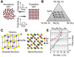
In the crystalline phase, GST alloys form a cubic lattice similar to that of a rocksalt structure (Figure 1C) in which Te atoms occupy one lattice site and the Ge/Sb atoms randomly occupy the remaining lattice sites. However, fast crystallization cycles locally distort the ideal cubic structure shown in Figure 1C. Moreover, most studied GST-based PCMs contain up to 25% vacancy-type defects in the Ge/Sb sublattice Nonaka et al. (2000); Yamada and Matsunaga (2000), an important characteristic that seems to be directly linked to the switching properties of GST alloys. We note, however, that the cubic structure is a metastable phase (around 150 ∘C) that can further transition to a stable hexagonal structure once the Ge2Sb2Te5 alloy is heated to 310 ∘C, a transition that has been argued as a disadvantage for the 225 stoichiometry of GST alloys (i.e., Ge2Sb2Te5) Friedrich et al. (2000).
Unlike the crystalline phase, the arrangement of atoms in the amorphous phase is the subject of debate. Most studies have assumed that a-GST is locally similar to the crystalline phase, but it lacks the long-range atomic order observed in the crystalline phase. However, this notion has been challenged in several experimental X-ray spectroscopies that echo a pronounced difference in the local arrangement of atoms in amorphous and crystalline phases, that is: “the Ge atoms that occupy octahedral positions in the crystalline phase switch to tetrahedral coordination in the amorphous phase.” Wełnic et al. (2006); Kolobov et al. (2004). To explain the discrepancy between these two narratives, Welnic et al. conducted a density functional theory (DFT) study to identify possible atomic arrangements in Ge1Sb2Te4 as a representative stoichiometric GST alloy Wełnic et al. (2006). This study revealed that the Ge1Sb2Te4 alloy may establish two different crystal structures: (1) the distorted cubic structure with “octahedral” Ge bonds (as shown in Figure 1C) and (2) a spinel structure in which Ge atoms form “tetrahedral” bonds with Te atoms, while Sb/Te atoms occupy atomic sites identical to those in the rocksalt structure (see Figure 1D). Interestingly, the ground-sate energy of the cubic structure is only 30 meV per atom less than that of the spinel structure. Thus, the difference in reported local orders of a-GST may stem from the competition between two energetically similar structures with significantly different local atomic arrangements. In addition, the assumption of the spinel structure can successfully explain the increase in the larger bandgap of the amorphous phase as compared to the crystalline state with the cubic structure.
Switching the phase from a-GST to c-GST generally involves two events: nucleation of small crystallites and the subsequent growth of these crystalline domains Coombs et al. (1995). To the first order, the nucleation process is governed by the thermodynamics of the phase change (i.e., a temperature-controlled process), while the speed of the crystal growth is primarily governed by the kinetics of the phase change (i.e., the atomic motion of elements). At high temperatures, above (600 ∘C for Ge2Sb2Te5), GST is in a liquid (molten) phase with highly mobile atoms. Thus, crystallization of GST is thermodynamically allowed once the temperature drops below the melting point, and the probability of crystalline nucleation increases as the temperature further drops, reaching the maximum probability at the glass-transition temperature, . However, at low temperatures close to , the crystalline nuclei cannot efficiently grow because the atomic mobility is extremely small. Thus, fast crystallization of a-GST occurs at intermediate temperatures between and , which is 150-250 ∘C for the cubic structure and 300-350 ∘C for the hexagonal structure. It is uniquely interesting that a-GST alloys remain amorphous for over 10 years at room temperature, but the very same material can be crystallized in only 20 ns upon heating up to only a few hundred degrees of Celsius, a feature that can be hardly found in any other PCM outside chalcogenide glasses.
Here, we would like to emphasize that the crystallization of melt-quenched GST films is strikingly different than the crystallization of as-deposited films. In a detailed study, Coombs et al. showed that crystallization of as-deposited films proceeds through a nucleation-dominated process, while in the melt-quenched films crystallization is growth dominated Coombs et al. (1995). Apparently, the melt-quenching process leaves some subcritical crystalline domains in the amorphous matrix, so that the slow nucleation step can be bypassed in the subsequent re-crystallization cycles. Therefore, crystallization of a melt-quenched GST alloy is significantly faster than that of an as-deposited amorphous film. However, this study suggests that the application of a short pulse can pre-condition an as-deposited film so that it mimics the fast switching speed of a melt-quenched film. For instance, using a pre-conditioning laser pulse of 100 nsec width, the crystallization time of the GeTe film can be reduced from 1 sec to only 30 nsec, which reflects the switching of the crystallization mechanism from the nucleation-dominated mode to the growth-dominated mode. We note that the presence of residual crystalline nuclei in melt-quenched films could be explained based on the low interfacial energy between amorphous matrix and crystalline domains, as demonstrated in undercooling experiments performed on GST alloys Friedrich et al. (2001); Kalb et al. (2005).
The switching behavior and the optical/electronic property contrast, induced by the phase switching, can be customized by changing the composition of a chalcogenide PCM, primarily through the substitutional doping of isoelectronic elements (i.e., parenthesis in Figure 1B) in ternary GST alloys. For example, the doping of GST alloys with selenium (Se) atoms forms a quaternary Ge-Sb-Se-Te PCM that is referred to as GSST Zhang et al. (2019a). A recent study shows that an optimized addition of Se to the Ge2Sb2Te5 alloy can significantly reduce the optical loss in the near- to mid-IR spectral range. Indeed, the optimized GSST alloy (i.e., Ge2Sb2Se4Te1) shows a broadband transparency in the 1-18.5 m wavelength range, while offering a large refractive-index change (n 2) without a loss penalty (i.e., k 0). DFT calculations show that increasing the Se content widens the bandgap of the GSST alloy, leading to a smaller optical loss in the IR regime. In addition, compared to the GST alloys, GSST alloys show a smaller density of states close to band edges, which reduces the free-carrier absorption loss in the IR regime. Interestingly, the substitution of the Te by Se does not change the crystal structure of GSST as it still forms cubic (metastable) and hexagonal (stable) structures similar to the GST case.
Increasing the Se content in GSST monotonically increases the crystallization temperature, which translates into a better stability of the amorphous phase. However, this stability comes at a major drawback that is explained in further detail in Ref. Coombs et al. (1995), that is: the crystallization becomes significantly slower as the Se replaced the Te in a GST alloy. As shown in Figure 1E, the time needed for the onset of nucleation in as-deposited GSST (i.e., t0) and pre-conditioned GSST (i.e., t’) and the total time needed for the completion of the GSST crystallization (i.e., tc) monotonically increase with the Se content in the GSST. In fact, the tc increases from 20 ns in GST to 3 sec in a GSST alloy with only 25% Se content, showing more than a 100-fold reduction in the crystallization speed. An even slower crystallization speed can be expected in results reported in Ref. Zhang et al. (2019a), where Se content is even larger and reaches 80% in the optimized composition (i.e., Ge2Sb2Se4Te1). It is also interesting that the influence of pre-conditioning on the crystallization speed becomes weaker as the Se content is increasing (compare t0 and t’ in Figure 1E). The slower dynamics in GSST is attributed to the nucleation-dominated crystallization which is intrinsically sluggish Coombs et al. (1995).
The large optical contrast in GST-based PCMs stems from the pronounced change of local atomic arrangements, in which the Ge coordination switches between octahedral (in crystalline) and tetrahedral (in amorphous) bonds. Such an atomic change is reflected in the 7% volumetric expansion of the GST following the crystalline-to-amorphous conversion, as experimentally evidenced in X-ray diffraction measurements Njoroge et al. (2002). In addition, quantum mechanical calculations, using the Fermi’s golden rule, show that such a local structural alteration leads to a large change in the elements of the matrix that governs optical transitions between two initial and final states in GST-based PCMs Wełnic et al. (2007). Considering the central role of Ge atoms in the coordination change, one can expect that a larger Ge content in GST alloys provides a larger optical contrast, as can be seen in a comparison between, for instance, Ge8Sb2Te with n+ik -1.48+i1.35 and Ge2Sb2Te5 with n+ik -1.2+i1.05 at 405 nm wavelength Yamada et al. (2002). However, the exact mechanism behind this trend is not well understood. Welnic et al. suggest that a lower density of vacancies in GST alloys enhances the optical contrast, and the addition of the Ge may help in achieving this goal Wełnic et al. (2006). However, Kolobov et al. argue that the presence of the vacancies at Ge/Sb sites is an intrinsic part of the GST structure and the addition of the Ge will not reduce the vacancy density Kolobov et al. (2004). Experimental studies support this argument, as the addition of extra Ge/Sb atoms did not reduce vacancy sites and instead led to the phase segregation and the accumulation of extra Ge/Sb atoms at the grain boundaries Yamada and Matsunaga (2000); Privitera et al. (2003). It is very important to notice that the origin of the optical contrast in PCMs is strictly different from that of the covalent semiconductors (e.g., Si and GaAs) in which local atomic arrangements remain intact, and the optical contrast stems primarily from the smearing of electronic states and the formation of tail states in the bandgap of the amorphous phase.
Reevaluating the portfolio of successful PCMs shows common characteristics that can be further employed for the identification and, yet better, prediction of alternative PCMs. First, all identified PCMs show distorted octahedral structures. Second, a relatively large density of intrinsic vacancies seems to be mandatory for the structural stability. Third, unlike most semiconductors with sp3-hybridized bonds (i.e., tetrahedral coordination), atomic bonds in PCMs display p-type characteristics. The p-type bonding (i) guarantees the 6-fold coordination in the crystalline state, (ii) is prone to distortion (because it is weaker than sp3 bonds) which is necessary for the crystal stabilization, and (iii) can be easily broken for the fast switching of bonds from octahedral to tetrahedra on amorphization. Interestingly, p-type bonding has been shown to occur in alloys with more than 4 valance electrons Luo and Wuttig (2004). Thus, considering these similarities, the search for new PCMs can be narrowed down to the alloys of group 15 and 16 with octahedra structures, more than 4 valance electrons, and proper Tg and Tm values. Also, special attention should also be paid to the specific stoichiometry of PCM alloys to eliminate the phase segregation during phase-transition cycles, if the fast switching speeds are desired. Though, for an ultimate search, the development of a robust model for the amorphous phase seems mandatory for the prediction of the novel PCM materials using the first principle calculations.
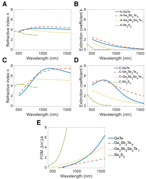
The holy grail of the optical modulation/switching is the large change in optical constants, and more specifically the refractive index of active regions in photonic devices. In Figure 2, we have presented real and imaginary parts of the refractive index for some promising chalcogenide-based PCMs, including two promising binary compounds, GeTe and Sb2S3. Ideally, a PCM with a large n and a small k is desired. As described by the well-known Kramers-Kronig relation, however, the real and imaginary parts of the refractive index are not independently controllable. Thus, the relative ratio of the index change to the loss change (i.e., n/k) serves as a figure of merit (FOM) for comparing various PCMs. As shown in Figure 2E, for operation in visible, NIR, and telecommunication wavelength (i.e., 1.55 m), Sb2S3, GeTe, and Ge2Sb2Se4Te1 provide the best FOMs, respectively. We note that such a conclusion is solely made based on the FOM. However, based on the switching speed, for instance, Ge2Sb2Te5 offers a faster response than both Ge2Sb2Se4Te1 and GeTe. Therefore, in the selection of PCM materials, the ultimate application should be considered.
We would like to mention that the inclusion of PCM materials in optical device platforms (discussed below) necessitates several fabrication considerations beyond the intrinsic material properties. First, most GST-based PCMs are prone to rapid oxidation upon long ambient exposures. Thus, PCMs are usually capped by a protecting layer (e.g., SiO2, Ta2O5, ZnS, ITO, etc.) that can withstand high-temperature phase switching events as well as fulfill the requirements of conversion stimuli (i.e., electrical vs optical). Second, in some cases, an irreversible diffusion of metal atoms into PCMs may be expected, which degrades the phase switching behavior in hybrid metal-PCM devices (e.g., plasmonic platforms). Addition of a diffusion-barrier layer or the use of alternative plasmonic metals (e.g., TiN) Lu et al. (2019) can fix this issue. We note that the addition of capping/diffusion-barrier layers may affect the details of the phase conversion in PCMs, probably because of modifying the nucleation/growth of crystalline domains as the interfacial energies at amorphous-crystalline, amorphous-capping layer, and the crystalline-capping layer will be modified. Such effects may be behind the reported change of the crystallization temperature following the capping of the Ge2Sb2Te5 alloy with ZnS-SiO2 capping layers Friedrich et al. (2001). Finally, device architectures should support fast thermal time-constants to allow for the rapid temperature change (109 ∘C/sec) needed for the amorphization via the melt-quenching, a factor that calls for the use of materials with proper thermal coefficients (e.g., thermal conductance, heat capacitance, etc.).
III Active Amplitude control with tunable phase-change metasurfaces
III.1 Hybrid plasmonic/PCM metasurfaces for global amplitude control
To highlight the unique capabilities of PCMs in meta-optic applications, early studies leveraged an easy-to-fabricate layer of PCM as the functional material. Although later rather complex patterned PCM nanostructures were utilized, so far, a vast majority of demonstrations of optical functionalities has been limited to the global control of PCMs across the entire MS. Herein, a comprehensive review of developed hybrid plasmonic and dielectric MSs using PCMs for global amplitude control is presented. Throughout this review, the so-called modulation depth (MD) and extinction ratio (ER) are considered as quantitative representations of the amplitude modulation of the reflected, transmitted, or absorbed light. For the reflected light, MD is defined as as the difference between the maximum reflected power (P) and the minimum reflected power (P) normalized by the incident power value (P) at a specific wavelength, i.e., MD = (P - P)/P. Moreover, ER is described in terms of the logarithm of the ratio of the maximum to the minimum reflected power, i.e., ER = -10 log10(P/P). It is noteworthy that based on the operation principle of the device under test, P and P are associated with either amorphous, semi-crystalline, or fully crystalline state of PCMs.
Hybrid PCM-plasmonic MSs have been considered as a promising set of candidates for the real-time control of the key properties of light due to the high sensitivity of metallic nanoantennas to the ambient changes. Such striking sensitivity originates from the spanned nature of localized surface plasmon resonance modes which are concentrated outside of nanoantennas. Based on the first-order perturbation theory, the resonance frequency change is governed by , in which is the total electric field and is the induced change of the dielectric permittivity and the integration spans over the unit-cell of a MS Johnson et al. (2002). Accordingly, the phase transition in the PCM in contact with the meta-atoms significantly influences the effective permittivity of the unit-cell and thus the resonance behavior, which enables the spatio-temporal and/or spectro-temporal control of the incident light.
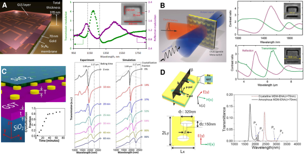
In a pioneering work by Samson et al., an innovative electro-optic switch by employing a homogeneous plasmonic MS composed of a periodic array of Au asymmetrically split resonators covered with a thin layer of GLS is implemented (see Figure 3A) Sámson et al. (2010). By applying electrical pulses, 10 ms duration and 45 V amplitude, to the electrodes connected to the embedded 200-nm-thick GLS film and the patterned metallic layer, up to 150 nm blueshift in the narrowband Fano resonance is observed in the near-IR wavelength range. This large tuning range stems from the significant refractive-index contrast of GLS after its uniform phase transition from the amorphous to the crystalline state. Such an ultrathin configuration provides a transmission modulation with a contrast ratio of 4:1 upon phase-change of GLS. We note, however, that the reversible electrical switching was not reported in this work.
In a following work Gholipour et al. (2013), Gholipour et al. enhanced the resonance shift by replacing GLS with a layer of Ge2Sb2Te5 embedded between two ultrathin supporting layers of ZnS-SiO2 (see Figure 3B). They have shown a global reversible phase transition across a large area of the 15 nm-thick GST layer by applying a single laser pulse with varying durations and peak intensities. As a proof of concept, a 50 m beamwidth laser pulse of 0.1 mWm-2 intensity with the duration of 50 ns and 0.25 mWm-2 with the duration of 100 ns have been exploited for amorphization and crystallization of the GST layer, respectively. Such an all-optical, bidirectional, and non-volatile MS offers a remarkable resonance shift of 200 nm with 2.5-fold MD in the transmitted near-IR light and 1.3 m resonance shift with 4-fold contrast ratio in the mid-IR band, respectively.
To demonstrate the potential of PCMs for the design of highly tunable MS optics, Chen et al. explored the use of intermediate phase transitions in Ge2Sb2Te5 integrated into a plasmonic crystal Chen et al. (2013). Their proposed structure consists of a 20-nm-thick PCM layer sandwiched between an array of Au disks and a quartz substrate, as shown in Figure 3C. To realize the stepwise nonvolatile tuning of the lattice resonance over a 500 nm range (from near- to mid-IR), the fabricated sample was uniformly baked on a hot plate for different time periods (up to 60 minutes) but at a fixed temperature of 135 ∘C. To reveal the relation between the crystallization fraction and the annealing time, the experimental results (i.e., optical reflection spectra) were theoretically reconstructed in full-wave simulations, a mapping scheme that gives an intuitive understanding between the degree of the phase change in the PCM layer and the optical response of the MS.
Following these pioneering reports, several other groups proposed alternative types of hybrid PCM-plasmonic architectures for the realizations of dynamic metadevices. Cao et al. published several theoretical proposals using Ge2Sb2Te5 for the tunable perfect absorption in the visible and mid-IR regimes Cao et al. (2014b, 2013a). They numerically demonstrated a tri-layer fishnet MS comprising of metal-PCM-metal elliptical nanoholes in a broken symmetry architecture and realized a narrow band Fano resonance (see Figure 3D) Cao et al. (2014a). To show the potential of the proposed configuration for high-speed all-optical switching applications, a comprehensive photothermal model was used to study the temporal variation of the temperature as the PCM film was exposed to ultrafast laser pulses. Their results showed that a low-intensity pump light with the fluence of 9.6 Wm-2 and pulse duration of 360 ps can convert the phase of a 160-nm-thick GST layer from the as-deposited to the crystalline state in a one-way fashion. Such a phase transition resulted in a 1 m tuning range of the supported Fano resonance mode with sharp transparency peaks in the mid-IR regime (see Figure 3D). In another work, the same group introduced a tri-layer planar chiral MS in the shape of a gammadion combined with a thin GST layer. Using this structure, they reported a large frequency shift of 58% (in mid-IR) for the circular dichroism, defined as the difference in the transmittance of right-handed and left-handed circularly-polarized light Cao et al. (2013b). Their opto-thermal model predicts 5 ns crystallization transition time to uniformly heat the 24-nm-thick GST layer to 883K through a low light intensity of 0.016 mWm-2.
New hybrid MS designs were explored by Rudé et al. for the demonstration of ultrafast (i.e., ps regime), broadband (up to 385 nm spectral shift), and large (up to 60% MD) optical tuning of the optical transmission in the vis-near-IR spectral range Rudé et al. (2016). As shown in Figure 4A, the investigated platform was formed by structuring a 2D array of nanoholes in an Au film underneath a thin layer of Ge2Sb2Te5 (20 nm). A remarkable modulation tuning of the extraordinary optical transmission (EOT) response using both thermal- and current-induced structural transitions was thoroughly discussed.
To promote the applicability of reconfigurable MSs in the C-band communications, Carrillo et al. demonstrated a 1D array of hybrid nanogratings for the amplitude modulation with a MD of 77% and an ER of 20 dB Carrillo et al. (2016). The proposed design benefits from an ITO capping layer for protecting a 60-nm-thick GST layer from the environmental oxidation while still allowing both optical and electrical access. Through a comprehensive sensitivity analysis considering the side effects of fabrication imperfections and critical design parameters on the metadevice performance, a systematic study of the optimization of the structural design was proposed. Furthermore, to explore the in situ switching of the PCM state, electro-thermal simulations using electrical pulses, applied between the top and bottom layers of the MS, were carried out. Regardless of the plasmonic metal type (Au, Al, W, and TiN), numerical results show that a 2.4 V and 50 ns RESET pulse with a 15/5 ns rise/fall time can uniformly amorphize the GST layer. On the other hand, for crystallization, a SET pulse of 1.4 V and 100 ns with a 30 ns rise/fall time was employed. It is worth noting that during the amorphization, the uniformly distributed temperature exceeds the melting point of GST (i.e., 600 ∘C), while during the crystallization cycle, the GST layer experiences 425 ∘C temperature, which is necessary for a rapid (a few tens of nanosecond) process. The same group later presented an experimental demonstration of a more practical architecture for the on-demand quality factor control Carrillo et al. (2018).
Dual-functional opto-electric nanoscale devices using PCMs have gained significant attention recently. Raeis Hosseini et al. took the advantage of a uniquely tunable metadevice framework with a bifunctional behavior; as a tunable MS for perfect absorption of visible light and as a resistive switching memory device for data storage Raeis-Hosseini and Rho (2019). The structure consists of an array of Ag nanosquares on a 25-nm-thick Ge2Sb2Te5 film deposited on the top of an Al-coated Pt mirror. Following the phase transformation, a narrowband (50 nm) to wideband (400 nm) perfect absorption in the visible spectral range and bipolar resistive switching with high ON/OFF ratio (106) occurs.
In contrary to the conventional metal-insulator-metal (MIM) tri-layer reflective MSs, Dong et al. experimentally demonstrated a transmissive MS by eliminating the bottom metal reflector Dong et al. (2018). The fabricated MS exhibits a transmission dip that can be switched from 3 to 6 m upon the phase transformation in a 65-nm-thick GST film on a hotplate. The sparse distribution of the nanosquare array significantly reduces the device capacitance and facilitates the nsec-order electrical switching speed of the GST layer. The proposed structure enables collinear filter design necessary for the spectrally selective microscale mid-IR hyperspectral imaging.
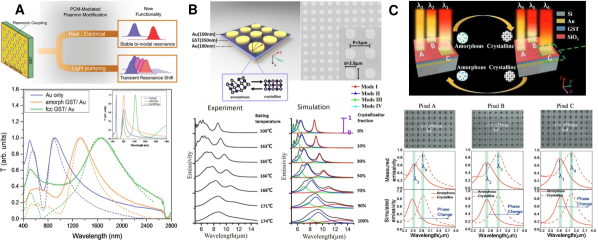
The ability to control the thermal emission from an object with subwavelength thickness has attracted a growing interest to a wide range of applications, including radiative cooling and energy harvesting Julian et al. (2019). According to the Kirchhoff’s law, the absorptivity of material equals its emissivity at equilibrium conditions, thus MS absorbers can be employed as thermal emitters within the mid-IR spectral band Baranov et al. (2019). Qu et al. utilized an MIM architecture (as shown in Figure 4B) incorporating a 350-nm-thick Ge2Sb2Te5 layer to dynamically manipulate the thermal emission with zero-static power Qu et al. (2017). By baking the sample on a hot plate for a fixed time period of 60 seconds at varying temperatures, the emissivity, bandwidth, and peak wavelength can be finely tuned. In a follow-up work Qu et al. (2018a), they developed a dual-band thermal emitter with an engineered array of Au nanoellipses to excite higher-order magnetic resonances with a perpendicular polarization along short and long axes. The polarization of the thermal emission is rotated by 90∘ at the 9.55 m peak wavelength upon the partial conversion of the PCM film (40% crystallization fraction). Inspired by these initial studies, several exciting technologies such as wide-angle and near-perfect dynamic thermal camouflage devices Du et al. (2017) and switchable and wavelength-selective thermal emitters Qu et al. (2018b); Du et al. (2018) were demonstrated.
More recently, multispectral thermal emission using a PCM-plasmonic MS in the mid-IR wavelength range (2-3 m) was studied Cao et al. (2018). The MIM architecture is formed by the arrangement of three distinct pixels where each pixel consists of uniform Au nanosquares with a different width designed to radiate at a distinct wavelength (see Figure 4C). The developed multiphysics heat transfer model shows that the reversible switching of perfect emissivity between two distinct wavelengths can be achieved by the phase transition in a 50-nm-thick Ge2Sb2Te5 within only 300 ns.
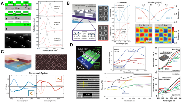
The introduction of new PCMs with higher optical contrasts and lower loss in the mid-IR regime (such as Ge3Sb2Te6) made another avenue for the realization of dynamic MSs with a stronger tunability range. Authors in Ref. Michel et al. (2013) studied the behavior of PCM-plasmonic MSs with three different configurations: Al nanoantennas arrays underneath, inside, or on top of a sputtered 50 nm-thick PCM layer (see Figure 5A). The proposed structure relies on the Wood’s anomaly to achieve a narrowband resonance for switching applications. Indeed, in a lattice of resonant nanoantennas, the interference between the nanoantenna resonance and the Bragg resonance of the lattice generates narrow resonances. Experimental results show that, upon the structural transition of the PCM, a large tuning range to the full width at half maximum (FWHM) ratio (about 1.03) can be achieved. Michel et al. later demonstrated the reversible tuning of these resonances by using ultrafast laser pulses as the stimulation source for the phase conversion in Ge3Sb2Te6 Michel et al. (2014). They used 800 nm femtosecond pulses with a 1.65 mJ energy per pulse, a 50 fs pulse width, and repetition rates up to 960 Hz focused at 230-270 m area on the sample. Moreover, to improve the optical functionalities and simplify the fabrication process, they avoided the deposition of capping and buffer layers.
In several applications, such as perfect absorption and thermal emission, Ohmic losses within the constitutive materials are favorable to enhance the overall performance of the optical device and its figure of merit (FOM). In this regard, Tittl et al. presented the first experimental demonstration of a band- and consequently temperature-selective switchable mid-IR perfect absorber Tittl et al. (2015). As depicted in Figure 5B, their proposed structure is a MIM architecture composed of a spacer layer of Ge3Sb2Te6 sandwiched between an Al back reflector and an array of Al nanosquares. Thanks to the strong gap surface plasmon (GSP) mode, nearly perfect absorption (90%) independent of the incident angle and polarization occurs. A resonance shift over 500 nm in the reflectance response upon the structural transition of GST from the amorphous to the crystalline state was experimentally realized. By simultaneously increasing the number of pixels and reducing the FWHM of the resonances, such an interesting platform offers diffraction-limited multispectral thermal imaging capability with high resolution (see the right panel of Figure 5B).
The first experimental demonstration of tunable chiral MSs using PCMs was reported by Yin et al. Yin et al. (2015). The authors leveraged the transparency window of Ge3Sb2Te6 (between 2.8 and 5.5 m) for large spectral tunability (from 4.15 to 4.90 m) of the circular dichroism (CD) response in the mid-IR regime. They utilized this effect in combination with a static chiral bias-type layer to flip the sign of the CD signal. The underlying system consists of a 50-nm-thick layer of PCM sandwiched between a Born-Kuhn type chiral plasmonic dimer comprising of corner-stacked nanorods (Figure 5C). The ease of fabrication with no additional lithography step and optimum near-field coupling of the generated localized surface plasmon with the functional materials are the two-fold advantages of this architecture.
So far, most MS optic applications have been incorporated in PCMs as a tunable dielectric medium. However, the inherent plasmonic properties, i.e., negative relative permittivity, of some PCMs upon transition from the amorphous to the crystalline state has gone somewhat overlooked. In 2018, Gholipour et al. demonstrated that upon transition of a 70-nm-thick structured layer of Ge2Sb2Te5 from amorphous to polycrystalline phase, the material functionality is switched from dielectric to the metallic (i.e., plasmonic) in the ultraviolet (UV) to near-vis spectral range Gholipour et al. (2018). As shown in Figure 5D (middle panel), while the real part of the relative permittivity of a-GST is positive at wavelengths below 660 nm, it exhibits negative values necessary for the generation of a surface plasmon polariton (SPP) mode. Figure 5D (middle panel) shows the plasmonic FOM, defined as the ratio of the real part of the propagating surface plasmon polariton wavevector to its imaginary part which is a representation of the SPP decay length, for the polycrystalline GST and a series of widely used noble metals. It is clear that in the UV to near-vis range, polycrystalline GST has comparable FOM values to their counterparts’ albeit surpassed by Al. The authors fabricated a hybrid MS using focused ion beam milling of a multistack ZnS-SiO2/GST/ZnS-SiO2 layer to create a 1D array of nanogratings on top of the glass substrate. In the case of TM-polarization (incident electric field perpendicular to the grooves), the MS introduces resonances for both extreme states of GST, which manifest themselves in the transmitted and reflected visible colors (inset in Figure 5D). In the as-deposited amorphous phase, there exist displacement current resonances owing to the contrast between the GST as a high index dielectric and the low-index ambient. However, for the crystalline phase, the fundamental mode is a plasmonic resonance regarding the opposing signs of relative permittivity at the interfaces between the GST and the surrounding dielectric medium. Thanks to the anisotropic nature of nanogratings, the resonant peaks disappear when the MS is illuminated with a TE-polarized (incident electric field parallel to the grooves) light. Accordingly, the patterned structure functions as an effective medium with a non-dispersive response.
III.2 Hybrid dielectric/PCM metasurfaces for global amplitude control
Plasmonic MSs governed by localized and lattice surface plasmon modes exhibit high dissipation losses, limited scattering cross-sections, and low efficiency. To mitigate these drawbacks, CMOS-compatible high-index and semiconductor MSs with a wealth of distinct optical resonances have been introduced as promising alternatives. In this regard, dynamic dielectric MSs that rely on high-contrast PCM nanostructures enabling adaptive functionalities have gained increased interest recently.
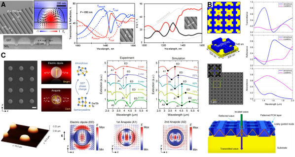
Karvounis et al. experimentally demonstrated bistable, rather high-quality transmission and reflection resonances using a 300-nm-thick array of non-diffractive sub-wavelength Ge2Sb2Te5 nanogratings (see Figure 6A) Karvounis et al. (2016). Upon TE-polarized excitation, anti-phase displacement currents along the GST core and a circulating magnetic field in the cross-section of the core occur (see Figure 6A). To tailor the electromagnetic response of the MS, GST nanogratings are converted from the amorphous to the crystalline state by raster scanning of a 532 nm continuous wave laser with a spot diameter of 0.5 m and intensity of 3 mWm-2. Such a structural transitions shift the initial near-IR resonance by as much as 10% providing switching contrast ratios of up to 5:1 (7 dB) in reflection and 1:3 (-5 dB) in transmission under a TE-polarized illumination (see Figure 6A, middle panel).
Pogrebnyakov et al. presented an optimized design and the experimental realization of a tunable polarization-insensitive MS using 150-nm-thick Ge2Sb2Te5 nanostructures to switch the optical functionality from a high transmittive filter to a highly absorptive device in the near-IR wavelength range Pogrebnyakov et al. (2018). As depicted in Figure 6B, the transmission resonance of the structure in the amorphous state is governed by a leaky guided-mode resonance induced by the periodic pattern of air voids within the GST layer. Due to the increased intrinsic loss of crystalline PCM, the field intensities in the structure is greatly reduced which results in transmission drop with a 7:1 contrast ratio.
Tian et al. performed a comprehensive mode analysis of structured phase-change alloys using the rigorous multipole decomposition technique Tian et al. (2019). The study shows that the high refractive index of Ge2Sb2Te5, coming with low loss in the mid-IR regime, empowers its nanostructure (which is a nanodisk) to support a diverse set of multipolar Mie resonances including ED, MD, and anapole state (see Figure 6C). Moreover, the dramatic optical contrast of GST enables dynamic controllability of these resonances leading to progressive spectral shifting of fundamental resonance modes. As a proof-of-concept, they showed that the ED-to-anapole shifting can be achieved by inducing 50% phase-change at any given wavelengths in the mid-IR spectral range (see Figure 6C). Multimodal shifting between the scattering bright and dark modes over a broadband region facilitates multispectral optical switching with high ERs. Notably, the intermediate phase transformation of the 220-nm-thick GST nanodisks was carried out by baking the sample on a hotplate with fixed temperature of 145 ∘C and different durations up to 9 minutes. Using a similar configuration, the same group demonstrated transmittance contrast up to 30 dB between two extreme phases of a 400-nm-thick GST nanodisk near the multipolar resonances in the mid-IR spectral range Tian et al. (2018).
Leveraging the optical contrast of PCMs, Petronijevic et al. demonstrated optical tuning of the electromagnetically induced transparency (EIT) effect in a Ge2Sb2Te5/Si MS Petronijevic and Sibilia (2016). The constitutive unit-cell is composed of a coupled dipole nanoantenna, which supports an electric dipole-like low-Q bright mode, and a square shape nanoring, which supports a magnetic dipole-like high-Q dark mode, hybridized by a thin (17 nm) layer of GST. When GST is in its amorphous state, an EIT-like transmission peak due to destructive interference of coupled modes in the transmission dip occurs. Crystallization of GST redshifts the resonances and destroys the EIT-like effect. Simulation results show a contrast ratio up to 10 in the telecommunication range. In a follow-up work, the same group utilized a 100-nm-thick layer of GeTe with structured Si nanobars to experimentally demonstrate switching of the collective dipole-like resonance of a hybrid MS with moderate contrast ratio (5) at the wavelength of 1.55 m Petronijevic et al. (2019). The crystallization process was carried out through slow heating of GeTe above its crystallization temperature ( 200∘C). More recently, several innovative hybrid MSs for active manipulation of fundamental resonance modes of constituent meta-atoms through the phase transition of embedded PCMs have been proposed Jafari and Rais-Zadeh (2016); Lan et al. (2019); Bai et al. (2019a, b).
Tian et al. demonstrated a polarization-insensitive broadband perfect absorber in the vis-near-IR region using a PCM-based MS. The MS is composed of an array of Ge2Sb2Te5 nanosquares separated from the Au mirror by a stack of low-index dielectric and high-index PCM layers. Thanks to the excited dipole/quadrupole resonances from the patterned GST structure and the cavity resonance mode from the GST planar cavity, near-perfect absorption peaks are achieved in the wavelength range from 350 to 1500 nm. A study on temporal variation of temperature through a heat transfer model revealed that the temperature of GST can be raised from room temperature to 480 K in just 0.56 ns with a light fluence of 1.11108 Wm-2. This not only lowers the power requirements for the phase transformation of PCMs but also decreases the crystallization process time to less than 1 ns.
Reconfigurable nanoscale optical cavities are promising candidates for applications such as displays and artificial retina devices. In a distinct, wide-angle display framework, Schlich et al. reported full color-switching by utilizing a thick multilayered reflective display incorporating a 18-nm-thick layer of Ge2Sb2Te5 on top Schlich et al. (2015). In their approach, a train of femtosecond laser pulses is employed to detune the resonance condition of the Fabry-Perot (F-P) cavity by transforming the phase of the GST layer. In another work, Yoo et al. leveraged a stack of PCM layers in an optical F-P cavity to generate a distinct artificial color spectrum Yoo et al. (2016). The highly absorbing nature of PCM layers combined with the strong optical interference effect governed by the cavity enables multiple color appearances by the selective phase transition of PCM layers. This concept was pursued by integrating a subwavelength optical cavity, which incorporated two separated layers of GeTe, with a joule heater element to produce a tunable micro-display rendering 4 different colors Jafari et al. (2019).
III.3 Hybrid plasmonic/PCM metasurfaces for local amplitude control
In the previous subsection, the adaptive functionalities are governed by global control on the amplitude of the incident light through a uniform structural transition of PCMs all over the metadevice. To harness the high potential of PCMs, local tuning of the individual meta-atoms in a reversible fashion is indispensable. In this subsection, recent developments enabling pixel-by-pixel programming of the MS using finely focused optical beams and localized electrical currents are discussed. We distinctly discuss both plasmonic and all-dielectric MS platforms with resonant and non-resonant meta-atoms exploiting PCMs to enable dynamic meta-optics.
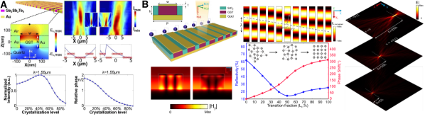
A bistable transmittive MS with a periodic arrangement of coupled Al nanopatches and 70-nm-thick Ge2Sb2Te5, as the dielectric spacer, was proposed to tune far-field radiation patterns in the mid-IR frequencies range Alaee et al. (2016). Numerical results show that GST with as-deposited state satisfies Kerker’s condition, in which constructive (destructive) interference occurs between the radiation of the electric and magnetic dipoles in forward (backward) direction, while the crystalline state only supports electric dipole resonance mode. As a result, the directive radiation pattern in the amorphous state is transformed into the omnidirectional scattering upon switching the state of the PCM layer to the crystalline.
Recently, Michel et al. demonstrated that phase switching of the PCM with localized laser spots can arbitrarily tune the resonance of an individual hybrid meta-atom up to one FWHM Michel et al. . The investigated MS is composed of a 2D arrangement of Al nanorods deposited on a Si substrate and covered by a 75-nm-thick Ge3Sb2Te6 layer which is protected by a thin capping film of ZnS-SiO2 (see Figure 7A). A semiconductor laser diode (660 nm central wavelength, sub-microsecond pulse duration) generating an elliptical beam spot, that is matched to the elongated shape of the nanorod, was employed for the writing process. While the aspect ratio of the long to the short axis (i.e., a/b) was kept constant during the experiments, the size of the elliptical beam spot was modified by changing the laser pulse power. As shown in Figure 7A (right bottom), by increasing the laser spot size, the resonance frequency redshifts from 4.98 m (vertical light blue line) in the amorphous state to 5.84 m (vertical light yellow line) in the fully crystalline case. Comprehensive simulations and experiments were performed to reveal the complicated relationship between the crystallization depth and the temperature gradient in the PCM layer. Figure 7A (right-top) depicts the resonance shifts for each crystallization depth (i.e., d) as a function of spot size (i.e., a) achieved from self-consistent multiphysics simulations. These findings show that through simultaneous control of the lateral size, crystallization depth, and position of the optically induced crystalline spot within each unit-cell, precise tuning of the reflection amplitude shift (less than 1 m here) and phase shift (less than here) can be achieved.
Utilizing a MIM structure confining a thin layer of GeTe, a tunable optoelectronic color generation system was proposed more recently Carrillo et al. . In the crystalline state, the gap plasmon mode characterized by mirrored currents in the top and bottom Al layers excites a transversal magnetic dipole mode that absorbs the incident light (see Figure 7B). Given the optimized geometrical parameters, such a resonant absorber can selectively absorb the red, green, and blue spectral bands of the visible spectrum and generate vivid cyan, magenta, and yellow pixels. By switching the state of the PCM to the amorphous phase, the resonant peak is suppressed and a reflective pseudo-white color is realized. Figure 7B illustrates a binary image composed of amorphous (with pseudo-white color) and crystalline (with cyan color) pixels generated using the experimentally measured spectra (right-top) and experimentally achieved from the fabricated MS written using a scanning laser (right bottom).
III.4 Hybrid dielectric/PCM metasurfaces for local amplitude control
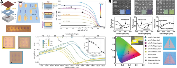
To highlight the potential of reprogrammable pixelated MSs, Hosseini et al. Hosseini et al. (2014) demonstrated the first representation of a high resolution, high speed, and low power consumption microdisplay (see Figure 8A). They employed a simple optoelectronic reflective framework in which a 7-nm-thick layer of Ge2Sb2Te5 is sandwiched between two layers of ITO as a transparent conductive oxide material. By applying electric current pulses through a conductive tip of an atomic force microscope (AFM), they switched the phase of GST from the amorphous to the crystalline in the nanometer scale. Due to the high optical contrast between the two solid states of GST, a vivid pattern of a color image can be imprinted using this technique. The authors improved the resolution of such color displays by replacing continuous films of ITO/GST/ITO with a crossbar type pixelated array of the same stack where each pixel can be randomly accessed and manipulated through the conductive AFM probe. To verify this, an array of subwavelength pixels (300 nm 300 nm with 200 nm pitch) was fabricated and electrically switched using a nanoscale conductive tip. Figure 8A shows the resulting optical images in which the optical contrast between the amorphous and crystalline pixels is striking. Reflective and semi-transparent type color displays with wide-viewing-angle were demonstrated on both rigid and flexible substrates. Also, to assess the electrical switching characteristics of a single pixel within a more easy-to-measure architecture, vertically crossbar-like ITO/GST/ITO devices with an active area of 300 nm300 nm were fabricated (see Figure 8A). The experimental current-voltage measurements show 350 times increase in the resistance between amorphous and crystalline phases at the threshold voltage of 2.2 V. Notably, a SET direct current can transform the device to its low resistance (or crystalline phase) while the amorphization process can be performed by applying a 100 ns RESET pulse and amplitude of 5 V to set back the device to its high resistance state. Later, the same group reported improvements in the off-line color depth modulation and resolution leveraging a similar approach and substituting Ge2Sb2Te5 with a growth dominant phase-change alloy Ag3In4Sb76Te17 (AIST) Ríos et al. (2016).
Wang et al. took benefit of multilevel crystallization state of PCMs in a stacked platform of dielectric/GST/dielectric to realize high-density optical data storage and grayscale holography Wang et al. (2014). Using a home-built optical system including an ultrafast pump-probe laser connected to a beam scanning apparatus, a grayscale image was written to the sandwiched 50-nm-thick Ge2Sb2Te5 layer. By reading out the reflectivity of a single pixel in the center of the written spot (0.64 m FWHM, 50 objective lens, NA = 0.8), a mapping between the crystallization level and number of induced laser pulses (with different pulse energies of 0.21, 0.28, and 0.36 nJ) was achieved (see Figure 8B). Given 730 nm wavelength writing laser and 1 m gird size, they also demonstrated a storage density of 1.7 Gbit/in.2 considering 8 distinct crystallization levels (equivalent to 3 bits/mark). Recently, the same group used a similar approach to imprint a grayscale image on a 70-nm-thick Ge2Sb2Te5 film, which was used later as a photomask with multilevel absorption Wang et al. (2017). This mask enables submicron lateral resolution grayscale photolithography to finely control the local exposure dosage necessary for 3D sculpting of photoresists used for fabrication of 3D MSs. Other groups have reported grayscale image recording by taking advantage of the multilevel structural evolution of PCMs induced by focused laser beams with different pulse energies Wei et al. (2017); Wen et al. (2018b). Also, computer-generated hologram patterns with 1 m pixel pitch and 16 k16 k resolution were realized by the local phase transition of a 20-nm-thick Ge2Sb2Te5 film Lee et al. (2017). This was accomplished by excimer laser (308 nm wavelength, 30 ns pulse width, 600 Hz repetition rate) photolithography with a fluence of 60–80 mJcm-2 on the surface of the PCM layer. The refractive index change due to the crystallization of GST shifts the resonance governed by thin-film interference condition in each pixel which can be applied to realize a broadband, full-color diffracting hologram panel. Recently, a rewritable full-color computer-generated hologram using PCM-based color-selective diffractive optical components has been demonstrated Hwang et al. (2018). The recorded spatial binary pattern in the Ge2Sb2Te5 layers combined with thickness-tailored substrates generate color-selective optical diffractions that can be tuned by inducing intermediate states in GST.
IV Active Phase control with tunable phase-change metasurfaces
The potential functionalities of reconfigurable PCM-based MSs discussed in the previous section are restricted to the amplitude modulation of the scattered light. To enable real-world, on-demand applications, dynamic optical components tailoring the phasefront of the incident light is essential. More recently, several groups have demonstrated tunable phase-gradient MSs employing PCMs, thereby extending the capability of dynamic wavefront shaping, such as reconfigurable beam-steering, tunable focusing, and switchable photonic spin-orbit interactions. In the following section, a review of the recent progress on the implementation of PCM-based MSs for active tuning of the phasefront of the scattered light is provided.
IV.1 Hybrid plasmonic/PCM metasurfaces for global phase control
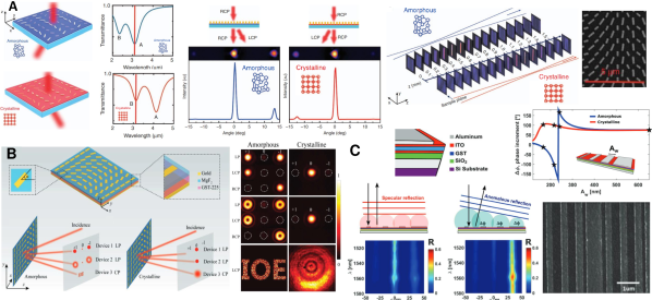
So far, the proposed dynamic MSs utilized resonant dispersive meta-atoms, which intrinsically limit the operational bandwidth of corresponding optical functionalities. To facilitate dispersionless phase control while making the scattered amplitude from the phase response decoupled, Pancharatnam-Berry (P-B) or geometric phase MSs have been introduced as an effective paradigm. By spatially varying the orientation of identical meta-atoms around their optical axis, not only wideband gradient MSs can be realized, but also the fabrication tolerance is alleviated. In this regard, Yin et al. demonstrated the first dynamic P-B based MS consisting of two differently sized interleaved meta-atoms arranged on top of a low-loss 50-nm-thick layer of Ge3Sb2Te6 Yin et al. (2017). As shown in Figure 9A, when the GST layer is in the amorphous state, the resonance condition is only fulfilled for meta-atoms with longer lengths. However, upon conversion of GST to the crystalline state, only meta-atoms with the shorter length strongly interact with the incident light at the same wavelength. This enables interweaving of two functionalities using two parallel rows of meta-atoms with appropriate lengths interleaved in a supercell architecture. As depicted in Figure 9A, by rotating the longer and shorter meta-atoms clockwise and counter-clockwise, respectively, an opposite phase gradients can be imparted to the transmitted circularly polarized (CP) light leading to a cross-polarized light with +1 and -1 order diffraction, respectively. Moreover, by encoding the quadratic phase distribution of cylindrical metalens in the spatial orientation of plasmonic meta-atoms, a bifocal focusing can be realized upon switching the state of GST, although the overall efficiencies are less than 10%. It is notable that resonant meta-atoms in the spatial multiplexed MSs have relative low scattering cross-section thus decreases the overall efficiency compared to the conventional schemes.
Zhang et al. have experimentally demonstrated switchable spin-orbit interactions using a hybrid P-B phase MS Zhang et al. (2018b). A MIM configuration is adopted in which the insulator layer is comprised of a thin layer of MgF2 on top of a 600-nm-thick Ge2Sb2Te5 film sandwiched between the bottom Au substrate and the top array of Au nanoantennas (see Figure 9B). Due to the judiciously engineered meta-atoms, when the GST is in the amorphous state, the reflectance of the cross-polarized light from the MS is as high as 60%, while the co-polarized reflectance is less than 10%. Accordingly, the MS exhibits a highly efficient half-wave plate functionality with the polarization conversion ratio (PCR) overcoming 80% in the mid-IR spectral range. By annealing the a-GST active layer and converting its state to the crystalline, the MS functions as a simple mirror with a relatively low PCR of 10%. The authors leveraged this effect to dynamically manipulate the coupling between spin and orbit momentums of photons in a broadband wavelength range from 8.5 to 10.5 m. As a proof-of-concept illustration, three MSs controlling the spin-orbit interactions were fabricated and characterized, which enabled spin Hall effect, vortex beam generation, and holography in the amorphous case (see Figure 9B). The state transition of the a-GST to the c-GST simply destroys the geometric phase phenomena and thus deactivates these optical functionalities.
More recently, de Galarreta et al. demonstrated a reconfigurable MS for beam steering applications in the operating spectral range of 1530–1570 nm de Galarreta et al. (2018). As shown in Figure 9C, the MS is comprised of SiO2, ITO, GST, and ITO multilayer stack sandwiched between an Al back reflector and a top array of periodically arranged Al nanoribbons with different lateral widths. The choice of Al as the plasmonic material not only reduces the fabrication cost but also makes the whole process CMOS compatible. Furthermore, the spacer layer between the nanoantennas and the PCM layer can be removed due to less diffusion of Al compared to Au in GST. This maximizes the interaction of the PCM layer with the near fields of the plasmonic nanoantennas. However, its relatively low melting temperature (around 660 ∘C) makes the amorphization process of the GST layer challenging due to possible deforming or even melting issues. It is notable that the MIM configuration not only supports the fundamentally enhanced GSP mode, characterized by the antiparallel displacement current, but also does the subwavelength feature of the dielectric spacers facilitate the quenching process during the amorphization. Herein, the gradient phase control is achieved by slightly detuning each nanoribbon width from the specified center resonant frequency (see Figure 9C). Beam steering with simultaneously multiple reflecting angles can also be achieved by pixelating the MS where each pixel can specifically be designed to steer the incident light at a different angle. When the GST is in its amorphous state, the MS functions as an anomalous reflector to a predesigned angle while in the crystalline state the incident beam experiences no phase gradient, and thus the incident light is specularly reflected.
IV.2 Hybrid dielectric/PCM metasurfaces for global phase control
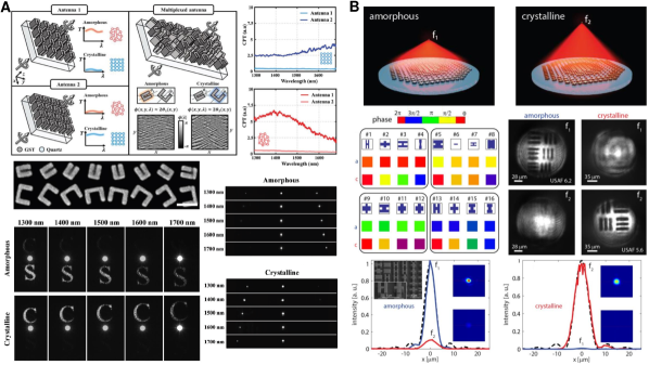
Choi et al. recently demonstrated wavefront switching in the near-IR spectral range utilizing a high-index MS comprising of an arrangement of rotating 260-nm-thick, U-shaped Ge2Sb2Te5 nanoantennas Choi et al. . As shown in Figure 10A, two types of nanoantennas are used, in which type 1 exhibits large cross-polarized light transmittance (CPT) in the amorphous state under CP light illumination while exhibiting near-zero CPT for the crystalline phase. On the other hand, type 2 is optimized to show the same performance in the crystalline and amorphous states, respectively. Leveraging a multiplexed supercell (with 1.16 m size) of both types of nanoantennas arranged based on the P-B phase principle, two distinct applications, i.e., anomalous refraction angle switching and dispersionless active hologram were implemented. As shown in Figure 10A, the nonresonant scattering characteristic of these engineered meta-atoms grants wide (over 500 nm) operational bandwidth and high signal-to-noise ratio (above 7 dB) adaptive functionalities. Furthermore, a reliable fabrication process for dry etching of a 260-nm-thick layer of GST to form nanostructures with sharp side walls was also provided.
More recently, Shalaginov et al. introduced an active metalens platform comprising of an array of judiciously patterned Ge2Sb2Se4Te1 Huygens meta-atoms sitting on top of a CaF2 substrate (see Figure 10B) Shalaginov et al. (2019). A generic design methodology enabling phase minimization error while maximizing the optical efficiency on the transformation of GSST from the amorphous to the crystalline state was presented. The continuous [0, 2] phase profiles required for the bifocal focusing in the amorphous (with NA = 0.45) and crystalline (with NA = 0.35) cases are discretized to 4 equidistant phase levels. Accordingly, 16 distinct meta-atoms are necessary to cover all possible combinations of phase jumps upon the structural transition of GSST. Through full-wave simulations, a library of Huygens meta-atoms with distinct geometries, including “I”, “H”, and “+”, was generated by sweeping the structural parameters to achieve the 16 optimal meta-atoms corresponding to 16 combinations of phases (see Figure 10B). Consequently, a bistable varifocal metalens with diffraction-limited performance (above 20% at both states) and low cross talk (switching contrast ratio of 29.5 dB) was experimentally demonstrated at the mid-IR wavelength range around m. For further validation, standard USAF 1951 resolution charts images were captured by a meta-lens in its two states. Figure 10B depicts that USAF 6.2 (half-period 8.8 m) and USAF 5.6 (half period 7.0 m) are greatly resolved in the amorphous and crystalline states, respectively, which are well-matched with the theoretical resolution limits of 9 m and 7 m, respectively.
IV.3 Hybrid plasmonic/PCM metasurfaces for local phase control
In 2015, Chen et al. demonstrated a hybrid metalens consisting of a 1D array of Au nanoslits filled with 100-nm-thick Ge2Sb2Te5 (see Figure 11A) Chen et al. (2015). Theoretical results show that the F-P resonance mode supported inside each slit can be spectrally adjusted by changing the crystallization fraction of the GST. This way, the phase of the transmitted light at the operating wavelength of 1.55 m can be controlled over a 0.56 range. However, in experiments, only two states of amorphous and fully crystalline can be achieved that limits the number of feasible optical phase patterns to two. The crystallization process is carried out through scanning of a laser beam (532 nm, 4 mW, focused by a 100 objective lens) along the slits at a speed of 0.2 /s. As a proof-of-concept demonstration, two distinct phase profiles were encoded into two different samples by selectively crystallizing the GST slits. Figure 11A illustrates the far-field patterns of on- and off-axis metalenses in comparison to an amorphous reference sample.
In Ref. Abdollahramezani et al. (2018a), the authors proposed a hybrid PCM-plasmonic MS to locally tailor the amplitude, phase, and polarization responses of the reflected light using a unique addressable MIM structure (see Figure 11B). They leveraged the two fundamental modes of the structure, i.e., short-range surface plasmon polariton coupled to the intermediate 180-nm-thick Ge2Sb2Te5 nanostripe, and the propagative surface plasmon polariton mode tunneling to the GST nanospacer (see Figure 11B). By taking advantage of the multistate phase transition of the GST, they have shown a drastic modification in the mutual interaction of such enhanced modes leading to an inherently broadband response. Electro-thermal simulations results show considerable control on the key properties of the reflected light in the near-IR spectral range; broadband, high-efficiency phase shift up to 315∘, and reasonable amplitude modulation up to 60%. A reconfigurable, high numerical aperture, and diffraction-limited varifocal metalens was implemented by addressing crystallization fraction of each meta-atom. The focal point can change from to while preserving the high-resolution feature comparable to the Airy disk (see Figure 11B).
IV.4 Hybrid dielectric/PCM metasurfaces for local phase control
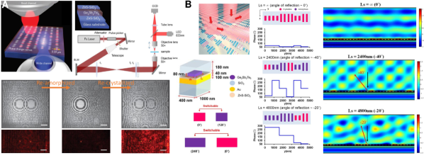
Employing high-speed optical pulses is an alternative approach for local conversion of PCM-based MSs as nanosecond and microsecond laser pulses were conventionally used in the optical data storage technology for robust reversible switching between the extreme state of PCMs. In 2015, Wang et al. successfully demonstrated multilevel switching of Ge2Sb2Te5 enabled by careful controlling of the energy and the number of stimulating optical pulses from a femtosecond laser Wang et al. (2016). They implemented this technology by developing a set-up consisting of a spatial light modulator for writing the optical pattern (with a diffraction-limited resolution of 0.59 m using an objective lens with NA = 0.8) and an imaging system for reading the exposed zones to optical pulses (see Figure 12A). The system used a pulse picker connected to a high-repetition-rate femtosecond laser (85 fs pulses with 85 MHz repetition rate at the wavelength of 730 nm) to control the intensity and duration of the femtosecond pulse trains. The experimental results show light-induced phase transition within an extremely small volume, down to 0.02 m3, of a 70-nm-thick GST layer sputtered on a glass substrate covered with a ZnS–SiO2 film, which is promising for realization of dynamic three-dimensional MSs. Several on-demand optical functionalities including bichromatic and multi-focus Fresnel zone plates, super-oscillatory lens, wavelength-multiplexed focusing lens, and hologram were imprinted to the same area without changing the structure of the optical system. Such a reprogrammable MS is enabled via writing, erasing, and rewriting of two-dimensional binary or greyscale patterns induced by sub-microscale phase transition of GST (see Figure 12A).
In 2016, Chu et al. proposed an all-dielectric MS consisting of an array of different-length Ge2Sb2Te5 nanobars that can be selectively reconfigured to locally control the phase profile of the incident light (see Figure 12b) Chu et al. (2016). In this sense, dynamic gradient MSs can be realized by varying the period of constituent super cells comprising of meta-atoms with amorphous, partial, and/or full crystalline states. Simulation results indicate high performance specular and anomalous reflection angle controlling by switching the material state of 180-nm-thick GST nanobars. Each GST nanobar here works as a dipole antenna, whose resonance condition is imposed by the refractive index of the induced crystallinity, capable of abruptly modulating the phase of the reflected wave (see Figure 12b).
Recently, a hybrid MS consisting of dielectric/PCM meta-atoms in which GST nanoposts are enclosed by Si nanorings was proposed to locally tailor the phase front of the transmitted light Abdollahramezani et al. (2018b). Such a novel scheme provides an enhanced electromagnetic field inside the core via the strong interference of optically induced electric and magnetic dipoles. The resulting rather high-Q resonance mode together with the large accessible refractive index changes due to the state transition of GST offer a remarkable phase shift of 325∘ and large transmittance (more than 0.6) at the operational wavelength of 1340 nm. Several optical functionalities using such a unique MS including bifocal focusing and anomalous transmission have been demonstrated.
Forouzmand et al. theoretically investigated a high-index MS consisting of a 1D array of Ge2Sb2Se4Te1 nanoribbons separated from the Au substrate with a thin film of low-index dielectric Forouzmand and Mosallaei (2018). By locally transforming the material state of each meta-atom using a focused optical beam, the strength and spectral position of ED and MD resonance modes governed the overall response of the meta-device can be modified at will. Relatively large phase agility () and high performance (more than 45%) are granted through operation in the the so-called off-resonance regime (around 1.55 m), where the inherent dissipative loss due to the pronounced light-matter interaction within the lossy PCM is suppressed. Dynamic control over the adaptive functionalities such as beam deflection can be achieved with such a platform.
V phase-change photonic Integrated circuits
The recent development of large-scale programmable Si photonic devices with small footprints, low power consumption, and high bandwidth (in contrast to the bandwidth-limited electronic circuits) is attributed to the massive progress in PICs Sun et al. (2015); Graydon (2016). Considering the features listed above, PCM-based PICs have the potential to revolutionize the architecture of next-generation computers and data storage systems. In the following subsections, we will first review recent progress on the implementation of integrated phase-change switches and modulators. Then, a comprehensive overview on the usage of these key elements in realization of on-demand applications including all-photonic memories, arithmetic processors, non-von Neumann computing platforms, and brain-inspired synaptic neural networks will be presented.
V.1 Integrated phase-change photonic switches and modulators
Switches and modulators play key roles in the PICs. Generally, these components are implemented using Mach-Zehnder interferometers (MZIs) (with wide operational bandwidth) Zhuang et al. (2015); Liu et al. (2016); Pérez et al. (2017) and microring resonators (with high modulation strength and narrow operational bandwidth but high sensitivity to the fabrication imperfections) Reed et al. (2010) through the plasma dispersion effect (with weak modulation of the refractive index) Lu et al. (2016a), the thermo-optic effect (suffering from large footprint, low speed, and high power consumption) Chen et al. (2016), or the electro-optic effect (with higher speed but suffering from less switching efficiency and the thermal drift). To overcome the aforementioned constraints for realization of high-performance, large-scale reconfigurable integrated photonic networks, an ideal switch needs to have three important features: low static and dynamic power consumption, high switching contrast, and ultrafast switching rate. In this regard, PCMs, due to their desirable characteristics such as non-volatility (which retains the material phase without keeping the external stimulus active), high refractive index contrast between the amorphous and crystalline states (resulting in high on-off ratio), ultrafast transition down to sub-nanoseconds Loke et al. (2012), data retention for years, and high cyclability up to switching cycles Burr et al. (2010) have been successfully demonstrated for realization of near-ideal integrated photonic switches Tanaka et al. (2012); Rudé et al. (2013); Ríos et al. (2015); Zheng et al. (2018); Wu et al. (2018); Xu et al. (2019).
The crucial issue in most integrated phase-change photonic switches is the phase transition of the incorporated PCM between its different phases. This phase transition can be performed by heating the PCM element using external heaters (thermal effect), optical pulses (photothermal effect), and electrical pulses (electrothermal effect). Each of these phase transition mechanisms determines the switching performance of the device enabling specific applications. Therefore, in this subsection, with a focus on the mechanism used for the phase transition of the PCM, we present a comprehensive review on the development of integrated phase-change photonic switches and modulators.
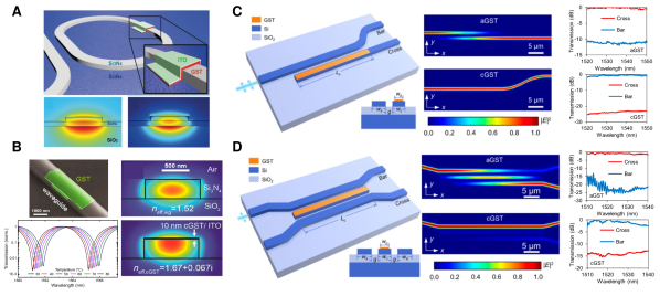
We start with integrated phase-change photonic switches based on the thermal annealing approach in which the incorporated PCM element is initially in its amorphous state, and switching occurs by slowly (using a hotplate) or quickly (using a rapid thermal processing (RTP) system) heating the sample so that the phase of the PCM is set to the crystalline state. This was experimentally demonstrated using an integrated photonic silicon nitride-on-insulator platform consisting of a nanophotonic Si3N4 bus waveguide which was coupled to a racetrack resonator partially covered by a Ge2Sb2Te5 thin film (see Figure 13A) Rios et al. (2014). The input light that is set at the resonance wavelength of the racetrack resonator (on-resonance) can be coupled to or isolated from the racetrack resonator based on the phase state of GST. In fact, the dramatic difference in the complex refractive index of the GST upon its phase change from amorphous to the crystalline state (performed by heating the sample at 200 ∘C for 3 min on a hotplate) strongly affects the attenuation inside the racetrack resonator, and in turn, changes the resonance condition by detuning the resonance wavelength of the racetrack resonator. In the low-loss amorphous case, the resonance condition of the racetrack resonator remains unchanged and the light propagates through the racetrack resonator as the a-GST film does not present (bottom left panel in Figure 13A). Therefore, the on-resonance input light traveling through the bus waveguide is critically coupled (where the round-trip loss rate is equal the coupling rate) to the racetrack resonator, and consequently, no power is transmitted to the output of the bus waveguide (transmission ‘0’). However, state transition to the highly absorptive crystalline phase increases the attenuation coefficient of the propagating mode inside the racetrack. This alters the resonance condition of the racetrack resonator, and thus, the off-resonance input light in the bus waveguide can no longer be coupled to the racetrack resonator and is completely transmitted into the output port of the bus waveguide (transmission ‘1’).
It is noteworthy that the determining factor in the operation of photonic phase-change switches is the heat-induced refractive index change of the PCM Rios et al. (2014); Ríos et al. (2015); Stegmaier et al. (2017). A discussion on the effect of annealing processes on the switching dynamics to optimize the switching performance is presented in Ref. Stegmaier et al. (2016). The authors studied the thermo-optical effect of a thin film of Ge2Sb2Te5 deposited on top of a Si3N4 waveguide as shown in Figure 13B. The waveguide is designed to ensure a single-mode operation when there is no GST on top (see the right top field profile). Even after the deposition of a thin layer of GST, the propagation condition does not tangibly change due to the low loss feature of the amorphous state. Upon transition of a-GST to its highly-absorptive crystalline phase, the effective complex refractive index changes which influences the evanescent coupling between the propagating light in the waveguide and the c-GST film and thus alters the waveguide mode (see the right bottom field profile). To study this thermo-optical effect, the authors used a transmission spectrum analysis of MZIs and a transient optical pump/probe measurement scheme for extracting the change in the imaginary and real parts of the refractive index of GST, respectively. The left bottom panel in Figure 13B shows the transmission spectrum of a MZI integrated with a GST element. A redshift in the spectrum and a decrease in the ER are observed upon heat-induced phase transition of GST.
While the resonator-based configuration presented in Figure 13A enables narrowband switching applications, other configurations have been investigated for broadband switching performance. In 2008, Ikuma et al. proposed a 22 integrated photonic switch using a short PCM waveguide placed between two Si waveguides in a directional coupler configuration in which the transmitted power through the bar and cross ports are controlled by the state of the Ge2Sb2Te5 Ikuma et al. (2008). Inspired by this work, some groups have demonstrated broadband directional coupler switches relying on the dramatic contrast in the extinction coefficient of the incorporated PCMs Zhang et al. (2018a); Xu et al. (2019); Olmo (2019). In 2019, Xu et al. experimentally implemented phase-change Si photonic 12 (see Figure 13C) and 22 (see Figure 13D) one-way switches by using an asymmetric directional coupler configuration incorporated with Ge2Sb2Te5 Xu et al. (2019). High bandwidth (more than 30 nm with -10 dB cross talk) and relatively low loss (1 dB) switching performance was demonstrated in the telecommunication band. The accurate phase transition of the PCM from its initial amorphous state to the crystalline state was performed by performing rapid thermal annealing of the device at 200 ∘C for 10 min under the flow of nitrogen to prevent oxidation. The switching operation for the case of the directional coupler 12 switch relies on the phase-match condition between the GST-on-Si hybrid waveguide (cross output) and the Si waveguide (bar output). For the low-loss a-GST, the effective refractive index of the TE mode in the hybrid waveguide is close to that of the Si waveguide (which is designed for the single-mode operation) resulting in an evanescent coupling of the input light from the Si waveguide (bar input port) to the hybrid waveguide (cross port) as shown in the middle top and right panels in Figure 13C. For the highly-absorptive c-GST, however, a strong phase-mismatch between the two waveguides happens due to the huge difference between their effective refractive indices. As a result, the input light in the Si waveguide is isolated from the hybrid waveguide and fully transferred to the bar output (see the middle bottom and right panels in Figure 13C). The operation principle for the directional coupler 22 switch can be explained similarly where coupling between the supermodes traveling through the three-waveguide system (two Si waveguides as cross and bar waveguides with one GST-on-Si hybrid waveguide as shown in the left panel of Figure 13D) can be modified by controlling the GST phase. When GST is in its amorphous state, the symmetric modes of the Si waveguides can be efficiently coupled to the antisymmetric mode of the hybrid waveguide due to the phase-matching condition. As a result, the input light from the first Si waveguide (bar waveguide) is completely coupled to the GST-on-Si hybrid waveguide, and then is fully coupled to the second Si waveguide (cross waveguide), and finally, fully delivered to the cross port (see the top middle and the right panels of Figure 13D). On the other hand, in the crystalline phase, the phase-matching condition is not met anymore which leads to the isolation of the input Si waveguide from the GST-on-Si hybrid waveguide, and thus transfers the light into the bar output (as shown in the bottom middle and the right panels of Figure 13D).
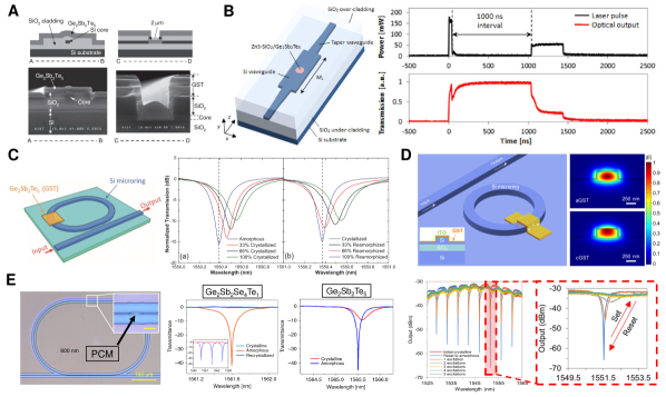
In a distinct work, a non-conventional chalcogenide PCM, namely GSST, with lower extinction coefficient than that of traditional GST alloys, was employed to demonstrate a similar functionality using a directional coupler configuration Zhang et al. (2018a). The experimentally measured results show broadband integrated photonic 12 and 22 switches with low insertion loss (0.01 to 0.4 dB in the C-band) and cross talk (i.e., the contrast ratio between the on/off- state at the output ports) over 15 dB ( 25 dB at 1550 nm).
Thermal treating of the PCM using a hotplate or RTP system is a slow process that makes such devices impractical for ultrafast switching applications. More importantly, it limits the device functionality to the one-way switching (from initial amorphous to crystalline) since the re-amorphization mechanism is a fast melt-quenching process, which cannot be performed using such simple bulky thermal heaters. Therefore, to realize the desired ultrafast and reversible (two-way) switching application, other means including optical and electrical pulses have been considered. We continue the review by discussing the recent developments using short optical and electrical pulses to reversibly change the state of PCMs, and then point out some recent researches investigated mixed-electro-optic effects for switching and modulation applications.
The optical excitation of the integrated PCM element can be performed using an out-plane focused laser beam or an in-plane guided laser light. While the former enables ultrafast switching performance, the latter adds many interesting fully-integrated on-chip applications such as on-chip all-photonic memories and mathematical operators. In the following, we first review those works used the free-space optical excitation approach, and then present some recent works utilizing an in-plane stimulus.
Ikuma et al. demonstrated a pioneering work on one-way optical gate switching by incorporating a thin layer of Ge2Sb2Te5 with a Si core waveguide (see the left panel in Figure 14A) working in the 1525-1600 nm wavelength window with MD of 12.5 dB Ikuma et al. (2010a). They used 660 nm free-space laser pulses with peak power of 89 mW and FWHM of 500 ns to switch the GST from its amorphous (on) state to crystalline (off) state. Later, they successfully demonstrated a reversible optical gate switch consisting of a shallow-etched Si core waveguide formed on a silicon-on-insulator (SOI) substrate and covered by a thin layer of Ge2Sb2Te5 (see the right panel in Figure 14A), working in the same operational wavelength range Ikuma et al. (2010b). They used an out-plane illumination with a peak power of 19 mW/94 mW (453 ns/8.4 ns FWHM) for crystallization/re-amorphization processes.
Since in Refs. Ikuma et al. (2010a) and Ikuma et al. (2010b) the size of GST elements are larger than the laser spot size, a semi-crystalline zone appears around the beam spot that increases the insertion loss. To overcome this drawback, the authors leveraged a multimode interference (MMI) Si waveguide integrated with a Ge2Sb2Te5 nanodisk (with a diameter of 1 m) covered by a ZnS-SiO2 capping layer (see Figure 14B) Tanaka et al. (2012). The operation principle of such a reversible optical gate switch with a wide operating wavelength range of 100 nm around 1575 nm is shown in the right panel of Figure 14B. The GST is initially in its off-state where c-GST with high extinction coefficient significantly absorbs the propagating light resulting in a near-zero power transmission. On the other hand, the low-loss a-GST allows propagation of light in the waveguide with a high optical transmittance (). The amorphization (switching from off- to on-state) is performed by irradiating the GST element using a laser pulse with a width of 40 ns and a peak power of 160 mW. To set back the state of the switch to its initial off-state (i.e., the re-crystallization process), a laser pulse with a width of 400 ns and a peak power of 50 mW was used.
Instead of relying on the difference in the imaginary part of the refractive indices of the two material phases, Rude et al. benefited from the remarkable change in the real part of the refractive index of Ge2Sb2Te5 ( while at = 1.55 m as shown in Figure 2). They experimentally implemented a reversible optical switch comprising of a Si racetrack resonator partially covered by a thin layer of GSt and coupled to a bus waveguide as shown in Figure 14C Rudé et al. (2013). An out-plane focused illumination from a nm diode laser with laser power of 12 mW (45 mW), pulse duration of 300 ns (20 ns), FWHM of 80 ns (8 ns) for crystallization (re-amorphization) of a 1 m diameter GST element was used. This way, the authors could reversibly modulate the optical path of the microring resonator and consequently, tune the resonance frequency of the racetrack resonator. Experimental measurements show switching operation at telecommunication wavelengths (around m) with MD of 12 dB (see Figure 14C).
Recently, Zheng et al. demonstrated broadband, fast, and reversible optical amplitude and phase modulation in a hybrid integrated photonic platform (see Figure 14D) Zheng et al. (2018). The simulated mode profiles of the hybrid waveguide at 1550 nm show a dramatic modification of the light mode attributed to the phase transition of the evanescently coupled Ge2Sb2Te5 nanostrip. The GST is initially in the highly-absorptive crystalline state resulting in a high optical transmission at the output (see the lower panel in Figure 14D). The state of GST can be controlled by short (440 ps) optical pulses in a two-way process. While a single reset pulse with effective energy (with respect to the effective area of the GST strip under illumination of a m diameter laser spot) of 620 pJ (9 aJ/nm3) was used for amorphization, a train of same duration pulses with 200 pJ energy (3 aJ/nm3) could re-crystalline GST. By varying the number of pulses, reversible (from amorphous to initial crystalline state) and quasi-continuous (from amorphous to several intermediate states) switching operation with a high ER up to 33 dB was shown (see the lower panel in Figure 14D). However, due to the high absorptive behavior of c-GST at nm, this device rendered low quality factor resonances Rios et al. (2014); Zheng et al. (2018); Cao and Cen (2019).
So far, the majority of works have benefited from the dramatic refractive index and extinction coefficient contrast (i.e., and ) due to the unique non-volatile phase-transition in PCMs. However, this limits the switching performance of PCM-based nanophotonic devices due to the low figure of merit (FOM), defined as , of PCMs. To outperform previous integrated photonic switches, more recently, Zhang et al. used Ge2Sb2Se4Te1 featuring low optical losses in a wide wavelength range of 1-18.5 m with a large refractive index contrast of resulting a large FOM. By using a hybrid SiN ring resonator (see the left panel in Figure 14E) reversible switching operation with a low insertion loss of 0.5 dB and record contrast ratio of 42 dB was experimentally demonstrated. They compared their results with a similar photonics platform employing Ge2Sb2Te5 as demonstrated by the middle and right diagrams in Figure 14E Zhang et al. (2019a). To show the repeatability of the switching operation, the GSST film was reversibly converted from amorphous to crystalline with 30 ns width (and 1s periodicity) pulses and crystalline to amorphous with a single 100-ns-width pulse.
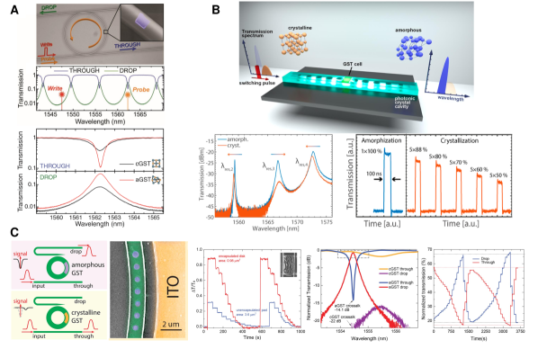
Hitherto, integrated photonic switches have employed an external bulky source to enable phase transformation of the functional material, which inhibits the realization of a fully integrated on-chip platform. In 2017, Stegmaier et al. demonstrated a pioneering fully integrated, reversible all-optical 12 switch Stegmaier et al. (2017). The proposed device is shown in Figure 15A in which a sub-micrometer Ge2Sb2Te5 element is placed on top of a ring resonator which is evanescently coupled to two parallel waveguides. The widths of the waveguides are appropriately designed to ensure the single-mode (TE-like) operation. If the input probe light wavelength is the same as the resonance wavelength of the ring resonator (on-resonance condition), the propagating light is partially coupled to the ring resonator and divided between DROP and THROUGH ports (see the orange marker in Figure 15A). On the other hand, the probe light with off-resonance wavelength is not coupled to the ring resonator and is fully directed to the THROUGH port. Therefore, by setting the probe signal on-resonance (at 1562.3 nm) and switching the phase of the GST element between low-loss amorphous state and highly-absorptive crystalline state, the ratio of the power coupled to the DROP and TROUGH ports can be controlled (see the lower panel in Figure 15A). For the initial case, the evanescent interaction between the c-GST element and propagating light in the ring resonator increases significantly. Accordingly, the loss within the ring resonator becomes more than the coupling loss to the waveguide leading to a weakly coupling regime between the ring resonator and the waveguide. Therefore, in the crystalline state, the on-resonant light is directed to the THROUGH port (black curve in the lower panel of Figure 15A). On the other hand, the on-resonance light (when GST is in the amorphous state) is completely coupled to the ring resonator and then fully transmitted to the DROP port (red traces in the lower panel in Figure 15A). This stems from the fact that the ring resonator is designed to be critically coupled to the waveguide (i.e., when the loss in the ring resonator is equal to the coupling loss) when the GST is in its low-loss amorphous phase. The probe signal used in this work consists of 500 ps optical pulses with 2.5 pJ energy (which are wide enough in width and low enough in energy to prevent any possible phase transition). The amorphization of the GST was performed by “write” signals consisting two 1 ps optical pulses (with 25 ns interval) of 95 pJ energy, while the re-crystallization was achieved using six groups of pulses with decreasing energy (each group contains one hundred 1 ps pulses with identical peak power) as described in Ref. Stegmaier et al. (2017).
With a simpler concept, later, Zhang et al. used a Si asymmetric MZI (AMZI) integrated with a micrometer-scale Ge2Sb2Te5 element on top of the ring resonator to boost the switching ER to more than 20 dB Zhang et al. (2018c). By controlling the number of pulses, the intermediate states of GST that enable tunable switching operation were demonstrated.
To improve the transmission contrast and power consumption of such integrated phase-change photonic switches, recently, Keitz et al. proposed to integrate a PCM element with a photonic crystal waveguide instead of a conventional bare photonic waveguide von Keitz et al. (2018). Figure 15B shows the proposed all-photonic reversible switch in which a sub-micrometer Ge2Sb2Te5 cell is placed on top of a photonic crystal waveguide and evanescently coupled to the center of a high quality factor photonic crystal cavity. The authors properly designed the photonic crystal cavities to guarantee high quality factor resonance modes (i.e., with minimum scattering losses) to enhance the interaction between the guided modes in the photonic crystal waveguide with the GST cell. As a result, when the GST cell is in its highly absorptive crystalline state, it more effectively absorbs the guided light. This enables a higher switching contrast with lower power consumption (14%) in comparison with the conventional integrated phase change photonic switches using a bare waveguide. Moreover, relying on the high refractive index contrast granted by GST, the authors showed the shift of resonance wavelengths that enables a tunable wavelength filter (see the bottom left panel in Figure 15B). While a single high-power pulse with 100 ns width can perform amorphization, a train of five consecutive groups of 100-ns-width pulses (each group contains five pulses with identical peak power that monotonically decreases in following groups) can re-crystallize the GST element (see the bottom right panel in Figure 15B).
The high-power optical pulses used in the previous works can cause deformation in the PCM cells which significantly increases the optical loss. To address this issue, recently, Wu et al. presented an innovative configuration by replacing the common rectangular GST cell with an array of subwavelength GST nanodisks (the seven blue circles in the false-colored SEM image shown in the left panel in Figure 15C) on top of a SiN microring resonator of an add-drop filter Wu et al. (2018). These Ge2Sb2Te5 nanodisks (with diameters of 500 nm) are encapsulated with a 50-nm-thick Al2O3 layer conformally grown by atomic layer deposition (ALD). The advantages of this configuration are twofold: (i) the pump light can heat the small GST nanodisks more uniformly than the relatively large micro-scale GST cell resulting in more efficient phase transformation, and (ii) the conformally deposited Al2O3 layer can minimize the surface energy when high-power optical pulses are used for phase transition of GST. Therefore, patterning and encapsulating processes can prevent the GST film from deformation. The authors also employed an array of five 10-nm-thick GST nanodisks placed on top of a simple Si3N4 waveguide to demonstrate reversible switching with less than 1 dB insertion loss and more than 20 dB contrast ratio in the telecommunication window. When the GST nanodisks are in their crystalline (amorphous) state, they significantly (negligibly) absorb the propagating probe light in the waveguide resulting in a low (high) optical transmission at the output. A single 50-ns-width optical pulse (220 pJ energy) was used for the amorphization of the five initially crystalline nanodisks. Also, trains of laser pulses for the stepwise re-crystallization process were employed in which each intermediate state was achieved by a train of 50 gradually decreased energy laser pulses with 50 ns duration each. This enables multilevel switching as shown in the left diagram of Figure 15C. For a systematic comparison, a traditional device in which a rectangular GST cell that fully covers the waveguide width was fabricated. The SEM observation (inset in the left diagram of Figure 15C) reveals that the GST film is deformed after the first high-power amorphization pulse which significantly reduces the transmission contrast (more than 50%). Figure 15C shows the operation principle of a switch designed near the critical coupling regime in which light is mostly delivered to the drop port when GST is in its low-loss amorphous state. The crystallization process largely redshifts the resonance of the microring resonator leading to high transmission in the through port (see the middle diagram in Figure 15C). In this work, the phase of the GST nanodisks can be stepwise controlled both optically and electrically. In the all-optical switching scheme, the amorphization is achieved by using a single “set” pulse with a width of 50 ns and total energy of 250 pJ (see the middle diagram in Figure 15C). On the other hand, in a stepwise re-crystallization process, the intermediate steps are realized using a train of 50 “reset” pulses (each with 50 ns duration) gradually decaying energy (see the middle diagram in Figure 15C). Due to the low absorption nature of a-GST, the re-crystallization process relies on high-energy pulses. To address this issue, a mixed electro-optic switching approach was proposed in which optical pulses with a width of 50 ns and total energy of 500 pJ are used for amorphization, while electrical pulses of 5 s duration and 1 V amplitude are applied to the underlying ITO heater (to provide a prolonged heating) for stepwise re-crystallization. This way, up to 20 intermediate transmission states enabling multilevel switching operation are achieved (see the right diagram in Figure 15C).
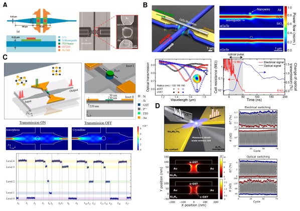
So far, realization of ultrafast, reversible phase-change photonic switches/modulators using on-chip and free-space laser pumps has been successfully demonstrated. However, these approaches cannot be practical for large-scale integration. For the former case, the alignment and focusing of the out-plane optical beam on the PCM inclusion is a slow process and constrained by diffraction-limitation of light. For the latter case, the routing process of the pump light and switching of a large-area PCM are cumbersome Feldmann et al. (2017). To address these limitations, recently, electro-optic Kato et al. (2017); Zhang et al. (2019c, b); Zheng et al. (2019) and mixed-mode electrical/optical Lu et al. (2016b); Farmakidis et al. (2019) approaches have been employed to enable reversible phase transformation of large PCM inclusions.
In 2017, Kato et al. experimentally demonstrated a current-driven reversible optical switch by integrating a m2 ITO microheater with a 30-nm-thick Ge2Sb2Te5 film on top of a MMI Si waveguide (see Figure 16A) Kato et al. (2017). The thickness of ITO was optimized to be 30 nm to reduce the switching energy while keeping the ER above 30 dB. By amorphization of both GST patches using a 100 ns current pulse of 20 mA, the propagating light experiences low loss resulting in high optical transmission (on-state). On the other hand, by re-crystallization of both GST patches using a 100 ms pulse of 12 mA, the probe light is highly absorbed resulting in a low optical transmission (off-state). An intermediate state was also obtained by amorphization of one GST patch, while maintaining the other one in the crystalline state. An average ER of 1.2 dB was experimentally demonstrated over the wavelength range of 1525-1625 nm.
In another work, Lu et al. experimentally studied a mixed-mode electro-optical switching operation by embedding a GeTe nanowire into a nanophotonic circuit Lu et al. (2016b) (see Figure 16B). The GeTe nanowire is evanescently coupled to a Si3N4 photonic waveguide and electrically contacted to two Au electrodes. While the former guides the optical signals sent by an off-chip fiber-coupled pump-probe setup for triggering/probing the state of GeTe nanowire, the latter enables electrical probing of GeTe phase through a RF setup. The reversible phase transition between amorphous and crystalline states of GeTe was carried out using nanosecond optical pump pulses. The state of the GeTe nanowire can simultaneously be measured through monitoring the intensity of the transmitted probe light and the slope of the I-V cure. As shown in the top right panel of Figure 16B, in the amorphous state, the resonant Mie scattering observed in the GeTe nanowire significantly enhances the light-matter interaction between the light propagating through the waveguide and evanescently-coupled GeTe nanowire (on-resonant). As a result, the transmitted power at the resonance wavelength is significantly reduced as depicted by transmission dips in the bottom left panel of Figure 16B. On the other hand, due to the dramatic refractive index change upon the state transition, the light is not coupled anymore to the crystalline GeTe nanowire (which is off-resonant) resulting in a high optical transmission. The bottom right panel in Figure 16B shows a decrease in the measured resistance (from 3 M to 6 k) and an increase in the optical transmission upon the full cross-sectional amorphization of the initially crystalline GeTe nanowire (with diameter of 300 nm) by using optical pump pulses with 50 ns duration and 10.7 nJ energy. To reset the switch, a 50 ns optical pump pulse with 6.2 nJ energy was used to re-crystallize the GeTe nanowire.
More recently, Zhang et al. experimentally demonstrated an optical memristive switch consisting of a MMI Si waveguide accommodating a Ge2Sb2Te5 nanodisk on top (see Figure 16C), which can be set/reset employing electrical pulses Zhang et al. (2019c, b). The top panels in Figure 16C show the structure of the switch in which a Si strip orthogonally crosses the center of the MMI, and is heavily P++-doped at the center, where GST presents. The 30-nm-thick GST nanodisk with a diameter of 1 m is covered by a 30-nm-thick layer of ITO film to prevent oxidation. By applying an electrical pulse, the doping stripe behaves as a resistive heater and transforms the state of GST. According to the self-imaging principle, the propagating light is focused into the center of the MMI, and so significantly interacts with the GST nanodisk leading to a high-performance switching. The optical power distributions in the MMI in the middle panels of Figure 16C show that the initially low-loss a-GST does not absorb the light resulting in a high optical transmission (on-state) while the highly-absorptive c-GST significantly absorbs the light leading to a low optical transmission (off-state). The authors showed that multilevel optical transmission levels in the off-state can be achieved through a stepwise crystallization process by either varying the pulse duration from 40 to 200 ns and fixing the amplitude to 3.5 V, or by varying the pulse amplitude from 3 to 6 V while fixing the pulse duration at 100 ns. This enables multistep switching performance with five distinct intermediate steps as shown in the bottom panel of Figure 16C. On the other hand, multiple optical transmission levels in the on-state can be achieved through a stepwise amoy7rphization process by using high power short electrical pulses with fixed duration of 20 ns and varying amplitude from 11 to 11.8 V, or a fixed amplitude but varying duration from 10 to 20 ns.
Although the architecture presented in Ref. Lu et al. (2016b) enables mixed-mode readout, it is based on using either optical or electrical set/reset pulses, and not both, to realize switching. In Ref. Farmakidis et al. (2019), the authors demonstrated not only both optical (transmission) and electrical (resistance) readout, but set/reset operations in a single device suitable for hybrid optoelectronic computing platforms. In this work, Farmakidis et al. leveraged a small-footprint platform of an electrically connected nanoplasmonic structure intersecting with an integrated photonic waveguide. This not only benefits from the strong light-matter interaction and low-loss switching in a subwavelength regime but also enables both electrical and optical reversible switching and readout operations in a hybrid integrated phase-change binary/multilevel memory. The top left panel in Figure 16D shows the schematic of the proposed device in which a Si3N4 rib waveguide is coupled to a plasmonic nanogap (with a tapered geometry) filled with a 75-nm-thick Ge2Sb2Te5 film protected from environmental oxidation by a 5-nm-thick SiO2 capping layer. The state of GST can be reversibly switched between its amorphous (high resistance and low transmission) and crystalline (low resistance and high transmission) by sending either optical pulses through the waveguide or electrical pulses through the Au electrodes. The Si3N4 waveguide is coupled to a plasmonic MIM waveguide (formed by two Au electrodes and the portion of GST in the nanogap region as shown in the cross-section view in the bottom left panel of Figure 16D). The field enhancement inside the nanogap depends on the state of the GST. For the low-loss a-GST, the light propagating in the Si3N4 waveguide is strongly coupled to the nanogap region resulting in a strong field enhancement in that region (as shown in the bottom left panel in Figure 16D) and low optical transmission at the output. For highly absorptive c-GST, however, this coupling is highly reduced, resulting in a lower field enhancement (as the lower electric field intensity in Figure 16D demonstrates) and in turn, higher optical transmission. The right panels in Figure 16D show both the electrical (upper panel) and optical (lower panel) switching of the device which can be readout with both electrical means (i.e., the change in the device’s resistance between two Au electrodes) and optical means (i.e., the change in the optical transmission of the waveguide). For optical switching, partial crystallization of GST is performed by sending piecewise optical set pulses (7.5 mW peak power for 8 ns followed by 3 mW for 400 ns) through the waveguide while a single rectangular reset pulse with 7.5 mW peak power and 8 ns duration is used for re-amorphization. Moreover, the authors successfully demonstrated the electrical switching of the device by sending an electrical reset pulse with 10 ns duration (5 ns rise/fall time) and 350 mV peak amplitude through the Au contacts for re-amorphization. A triangular pulse with 5 ns rise and 500 ns fall time and 350 mV peak amplitude was used for the crystallization process. In both cases, a CW optical probe signal and a constant voltage source ( mV) were used to simultaneously monitor the change in transmission and resistance, respectively.
V.2 Integrated phase-change photonic binary and multilevel memories
We live in an era with the explosive growth of information. The volume of data generated from smart devices, internet, fundamental research, and advanced technologies is exponentially increasing and reaching to a volume beyond the capacity of available computing/storage paradigms. Classical computers use the von Neumann framework in which data are transferred between the central processing unit (CPU) and memory units for processing and storage, respectively. Thus, the constant exchange of data between CPU and memory units limits the overall computing efficiency and leads to a traffic jam widely referred to as the von Neumann bottleneck Zhang et al. (2019d); Zhai et al. (2018). This bottleneck can be efficiently addressed through the introduction of a new paradigm that enables simultaneous storage and processing (i.e., arithmetic operations) of data in a single unit. PCMs seem a perfect fit for such a paradigm. First, the non-volatile nature of the phase change can supply the storage need. Second, the stimulation pulses, used for the phase conversion in PCMs, can be cleverly employed as the command signals for the implementation of logic operations. In other words, the width, height, and even shape of a pulse can be used as various knobs for the manipulation of a PCM phase, in which the data is stored. Third, the use of optical pulses (as the stimulation) brings the superiority of the optical domain over the electrical domain, namely the ultrawide bandwidth, multiplexing capability, low residual crosstalk, and high-speed operation. In addition, with the integration of PCMs with the rich portfolio of optical components (e.g., waveguides, resonators, and switches) the data processing capabilities can be extended from a unit cell (i.e., a PCM segment) to the system level. Thus, reading, writing, manipulation, and routing of the information can be all performed in an all-photonic scheme, a trend that will set the stage for the next-generation processors including emerging quantum computers.
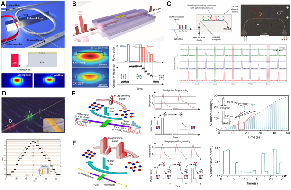
Optical property contrast, switching speed and minimum size of different optical states are the crucial parameters of PCMs for memory operation. Due to the dramatic optical contrast of GST over the visible and near-infrared spectral range, and its sub-nanosecond switching rate with high reproducibility and durability obtained over switching cycles Lencer et al. (2008), this alloy has been used as a suitable candidate for an integrated PCM photonics non-volatile memory. As the first demonstration, in 2012, Pernice et al. proposed an all-optical multilevel memory (in which the state of the GST can be changed from amorphous to different intermediate states) consisting of a microring resonator partially covered by a thin film of GST and coupled to a nanophotonic waveguide (see Figure 17A) all in a SiN platform to enable broadband optical applications Pernice and Bhaskaran (2012). A control port (the red SiN waveguide in Figure 17A) is used to deliver high-intensity optical pulses (with 600 fs width and less than 5.4 pJ for writing) for the phase switching (i.e., writing/erasing), and also to provide a low-intensity readout pulse for reading the states of the operating memory. When GST is in its low-loss amorphous state, the light traveling inside the microring resonator does not experience significant loss, so the propagating mode remains confined inside the SiN portion of the waveguide (see the bottom panel in Figure 17A) and the resonance condition of the microring resonator does not change. As a result, the input light is critically coupled to the ring resonator, and then, coupled to the Readout Drop port, resulting in a 0 transmission in the Readout Trough port (level ‘0’ of the memory or ‘erasing’). On the other hand, upon the switching of the GST to its highly-absorptive crystalline state, the traveling light is highly absorbed by the GST (see the mode profile in the lower panel in Figure 17A), which changes the resonance condition of the microring resonator (the resonance wavelength is different from that of the input light). Therefor, the input light can no longer be coupled to the microring resonator resulting in a 90 transmission in the Readout Through port (level ‘1’ of the memory or ‘writing’).
Recently, multilevel data storage was also achieved by Rios et al. via controlling the crystalline fraction in a PCM film. The authors used a simpler structure and experimentally demonstrated an eight-level memory with switching speeds of 1 GHz and switching energies of 13.4 pJ with the ability to arbitrarily switch between different intermediate states Ríos et al. (2015). Figure 17B shows the schematic of this functional layer. Since the GST cell is evanescently coupled to the waveguide, the phase state of the GST cell can determine the effective refractive index (see the bottom-left panel in Figure 17B), and accordingly, the optical attenuation through the waveguide. For switching the GST cell between its different states, high-power optical pulses are used. To amorphize (write) the GST cell, a single rectangular high-power pulse (with short width of 10 ns and switching energy of 13.4 pJ) is used (see the bottom-right panel in Figure 17B). Upon transition to the amorphous state, the low-loss GST cell does not absorb the passing light in the waveguide, leading to a high-transmission state (level ‘1’). On the other hand, a train of consecutive pulses with decreasing energy is used to perform a step-wise partial re-crystallization (erase) of the GST cell. When GST cell is in its fully crystalline state, the evanescent coupling between the waveguide and the highly-absorptive c-GST lead to a significant attenuation in the traveling light, resulting in a low-transmission state (level ‘0’). Therefore, the content of the memory cell is encoded in the state of the GST layer (i.e. ‘0’ in fully crystalline state and ‘1’ in amorphous state), or equivalently, stored in the intensity of the transmitted light at the readout port (‘0’ for low-transmission and ‘1’ for high-transmission). It is worth mentioning that partial re-crystallization of the GST using a single rectangular pulse is practically challenging because if the phase transition happens before the end of the pulse, the remaining optical energy can heat up the GST further to the melting temperature, and cause immediate re-amorphization. Therefore, by applying the erase scheme described above, they prevented the re-amorphization of already crystallized regions of the GST cell, and enabled access to intermediate re-crystallized states (or storage levels). For the readout of these states, we need to measure the degree of attenuation of the transmitted light associated with the level of re-crystallization of the GST cell. To do so, a single low-power light pulse (with 500 ps width and 0.480.03 pJ energy) is sent out along the waveguide, and the amount of the transmitted power identifies the state of the memory.
Authors in Ref. Ríos et al. (2015) further used the wavelength-division multiplexing (WDM) to demonstrate multi-wavelength operational schemes for accessing individual memory elements (see Figure 17C) Wright et al. (2019). To do so, they employed the wavelength-filtering property of three ring resonators with three different resonance frequencies ( 1 nm separation around 1550 nm) coupled to a bus waveguide. The design contains GST cells with a footprint of m2 deposited on top of the ring resonators as shown in Figure 17C. Since only on-resonance lights can be coupled to the ring resonators (i.e., no off-resonant coupling), the three memory cells can be addressed selectively for writing, erasing, and reading cycles. Using such WDM technique as well as the multilevel addressing, very recently, Feldmann et al. experimentally demonstrated the addressing of 256 memory elements to realize an all-photonic non-volatile memory with a storage capability of up to 512 bits of data in a array of memory elements.
In contrast to the approach in Ref. Ríos et al. (2015) (i.e., single pulse writing and multipulse erasing), Cheng et al. demonstrated that using a pulse-width modulation (PWM) approach, the efficiency of the re-crystallization process in terms of speed, energy and process control can be improved Cheng et al. (2018). Figure 17D demonstrates the concept of PWM switching in which optical pulses with different widths (), but with a fixed peak power (amplitude), are traveling through a waveguide to switch a GST cell evanescently coupled to the waveguide. By changing , the re-crystallization and amorphization of the GST can be controlled, leading to different levels of the memory (i.e, for level ‘0’, and for level ‘1’). More importantly, in their approach, each specific PWM sequence of pulses results in a particular re-crystallization state, independent of the starting state, meaning that each particular memory level can be directly accessed from any other stored level. As an example, Figure 17D shows a reversible 12-level memory implemented by a train of multiple () pulses with identical peak powers of mW and the periodicity of ns (inset in Figure 17D) but different widths from 5 to 20 ns. Each particular width is used for reaching to a different level. More interestingly, this approach was used for the realization of ‘OR’ and ‘NAND’ logic using integrated photonic devices, which is discussed in detail in the Ref. Cheng et al. (2018).
All the proposed all-photonic data storage/addressing schemes listed above are promising as they can reduce the latency related to the electronic memories, and the high power consumption for back-and-force electrical-to-optical data conversion. However, the use of multiple high power pulses for re-crystallization (erase command) not only slows down the programming operation, but more importantly, lowers the power efficiency and the signal-to-noise ratio, limiting the number of intermediate levels in the memory Rios et al. (2014); Feldmann et al. (2017); Ríos et al. (2019). To overcome these shortcomings, Li et al. proposed the same integrated photonic configuration to Ríos et al. (2015), but with a single double-step (dual-power) pulse for the erasing command (see Figure 17E). Using this modification, they successfully implemented a high-efficient multilevel memory with the ability to store up to 34 nonvolatile levels associated with over 5 bits Li et al. (2019). This multilevel operation was achieved by using a dual-pulse programming approach (see the left panel in Figure 17E) in which a fixed double-step erase pulse (with 250 ns width) was used for the step-wise crystallization, while a single rectangular writing pulse was used for amorphization (see the middle panel in Figure 17E). By monotonically increasing the amplitude of the programming pulse, they achieved 34 resolvable memory levels as shown in the right panel in Figure 17E. More interestingly, to enable arbitrary switching between the memory levels, authors used only one double-step pulse for both amorphization and re-crystallization (see the lower-left panel in Figure 17F). In this approach, the first part of the double-step pulse is used to remove the previous state of the memory by bringing the PCM above its melting temperature before re-crystallization (lower middle panel in Figure 17F). Then, by varying both the amplitude and width of the second part of the double-step pulse, arbitrary switching between different crystallization levels can be achieved (middle and right panel in Figure 17F).
We note that in studies listed above, GST was not included in the light path, but it was evanescently brought to its vicinity. The reason is that by placing the GST cell directly in the light path in the waveguide, the light passing through the GST cell would be significantly attenuated by highly absorptive c-GST, which significantly increases the power consumption of the device. Therefore, the GST cell is placed on top of the waveguide so that the light evanescently interacts with the GST cell.
V.3 Integrated phase-change photonic arithmetic processors
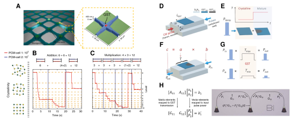
The multi-state scheme offered by the integration of non-volatile PCMs with nanophotonics can set the stage for an all-photonic computer in which the processing and storage operations can simultaneously occur in the same location. This is in contrast to the von Neumann approach in conventional computers in which the data is being continuously transferred between a CPU (for processing) and an external memory (for storage). In a representative demonstration, Feldmann et al. incorporated a GST cell at the crossing points of a rectangular waveguide array to enable independent manipulation of individual cells as shown in Figure 18A Feldmann et al. (2017). This abacus works based on the progressive crystallization of embedded PCMs and can perform arithmetic operations such as addition, multiplication, subtraction, and division, a set of operations required for a non-von Neumann arithmetic calculator. As an example, the operation principle of the addition of ‘’ in the base ten is represented in Figure 18B. Two PCM cells are used to represent the quantity of the first (red beads in the lower row of Figure 18B) and second (blue beads in the upper row of Figure 18B) digits of a two-digit system. These GST cells are initially in the amorphous states (high transmission) that represents the number zero. By performing a stepwise crystallization of the GST cell by using groups of identical picosecond pulses (each sets a predetermined crystallization fraction) different numbers are generated. In this case, each group consists of five consecutive pulses each with pulse energies of 12 pJ, and each group causes one crystallization step which is equal to one unit number. Due to operation in the base-10 system, the width and energies of the pulses are chosen such that 10 groups of pulses can fully crystallize the cell from its initial amorphous state, mimicking numbers 0 to 9 . Therefore, to perform ‘’, first, the level of the first PCM cell is set to six by sending six groups of pulses down to the waveguide. Then, to add the second summand of ‘’, more six groups of pulses are sent through the waveguide. Once the cell reaches to the 10th level, the device is reset (re-amorphized) to level 0 by using ten 19 pJ pulses. During the resetting of the first PCM-cell (to zero), the carryover of 10 is stored in the second PCM-cell by sending the corresponding pulse sequence and setting this cell to level 1. The resetting of the first cell and setting the second cell are carried out before applying the rest of the input sequence. Then, after applying remaining input sequences, the final states of the first and second cells are 2 and 1, respectively, representing the expected answer of 12 at the end of the calculation. This operation can be used for implementing other elementary operations by sequential addition (multiplication), addition of the nine’s complement of the second number to the first number (subtraction), and by sequential subtraction (division) Wright et al. (2019). An example of multiplication of ‘’ is shown in Figure 18C.
More recently, the implementation of scalar, and more interestingly, matrix-vector (MV) multiplication using integrated phase-change photonics are demonstrated Ríos et al. (2019). The MV multiplication is an important operation for modern data science such as image processing and machine learning. Figure 18D shows a photonic memory device consisting of a Si3N4/SiO2 waveguide with a thin layer of GST (10 nm) and an ITO capping layer (10 nm) atop. The transmittance state is determined by a write pulse used for amorphization and re-crystallization of the GST cell (Figure 18E). For the MV multiplication operation, several scalar multiplications each in the form of ‘’ should be performed. To implement this multiplication, instead of the successive addition in two PCM cells (as explained above), authors used a single PCM cell to directly carry out this multiplication. In their approach, the multiplier, , is mapped into the transmission state of the single cell (same as the previous approach), but the multiplicand, , is mapped into the power of an input pulse (see Figure 18F). Therefore, the multiplication is performed when the propagating light passes the evanescently coupled PCM cell, and the calculated result can be readout from the output power (see Figure 18G).
By designing an appropriate integrated photonic circuitry consisting of multiple PCM cells, the authors experimentally implemented the MV multiplication of a () matrix by a () vector which is shown in Figure 18H. Moreover, other form of arithmetic operations, such as logic operations can be performed, as described in details in Refs. Cheng et al. (2018); Youngblood et al. (2019).
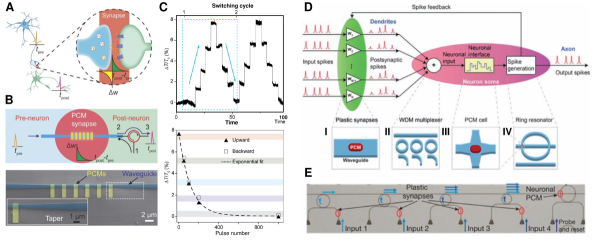
V.4 Integrated phase-change photonic synapses and neuromorphic processors
Another attractive capability of the integrated phase-change photonic platform is its ability to implement all-photonic synapses Cheng et al. (2017); Kuzum et al. (2013) and neurons Feldmann et al. (2019) as the central components for the hardware realization of brain-inspired neuromorphic computing which can enhance the efficiency of many important computational tasks, such as image processing, speech recognition, artificial intelligence, and deep learning, in terms of operation speed and energy consumption. The physical implementation of an integrated phase-change photonic synapse was first presented by Cheng et al. Cheng et al. (2017). Figure 19A presents the conceptual illustration of neurons and synapses. A neuron (pre-neuron) generates action potentials (or spikes with fire time ) that propagates along the axon and transmits through a junction to the next neuron (post-neuron) that generates the post-synaptic action potentials (fire time ). The junction is called a synapse (inset in Figure 19A) with the synaptic weight that determines the connection strength between the two neurons. The change in synaptic weight, , is called synaptic plasticity which is determined by neural co-activities and spike timing based on the well-known Hebbian learning or spike timing-dependent plasticity (STDP) rule. According to an asymmetric form of STDP, this synaptic plasticity has the form of , in which , and and are constants, meaning that a smaller (larger) spike timing difference results in a larger (smaller) increase in synaptic weight (inset in Figure 19A). The structure of the photonic synapse proposed by Cheng et al. is shown in Figure 19B which consists of a tapered SiN waveguide with evanescently coupled discrete Ge2Sb2Te5 islands on top enabling control over the optical transmission level which represents the synaptic weight. A low-power probe light (pre-synaptic spike) from pre-neuron passes through the photonic synapse and is directed to the post-neuron (from port 2 to port 3) by using an optical circulator (the red circle in Figure 19B). This circulator also guides the high-power optical pump pulses (working in a different wavelength from probe pulses) entered from port 1 to port 2 to change the synaptic weight. Before measuring the optical transmission, the PCM islands are at fully crystalline state (by annealing the device on a hotplate at 250 ∘C for 10 min) resulting in the optical transmission of which is defined as the baseline for readout and associated to a synaptic weight ‘’. The reason behind using multiple PCM islands (instead of a single patch) is the need for precise control of synaptic weighting, and more importantly, the ability to move between different crystallization levels using fixed-duration, fixed-power pulses (see the upper panel in Figure 19C). The authors in Ref. Cheng et al. (2017) showed that by varying the number of optical pulses sent down to the waveguide, fine control over the optical transmission change () and thus synaptic plasticity () can be achieved. More importantly, they showed that the change in the synaptic weight (or equivalently ) is exponentially and monotonically dependent on the number of optical pulses () applied, as shown in the lower panel in Figure 19C, which resembles the STDP rule. Therefore, by using an all-photonic structure based on an interferometer and fitting the exponential function of , where and are fitting constants, to the synaptic plasticity governed by the STDP rule (i.e., ), a correlation between an to mimic the STDP behavior can be developed.
In a follow-up work, Feldmann et al. implemented an all-photonic spiking neural network consisting of four neurons, sixty synapses, and 140 optical elements in total, a platform capable of supervised and unsupervised learning Feldmann et al. (2019). Figure 19D shows the schematic of the presented all-photonic network consisting of N pre-synaptic input neurons (which are not shown here) to generate the pre-synaptic input spikes, N interconnecting synapses (green region) to weight the pre-synaptic spikes, and one post-synaptic neuron (the red region) to receive the post-synaptic spikes and generate the output spikes. In this work, each synapse is implemented by a PCM cell placed on top of an optical waveguide in which the synaptic weighting (plasticity) is attributed to the phase transition of the synaptic PCM cell as described previously (panel I in Figure 19D). Then, the N input waveguides are coupled to N small ring resonators, each with a specific resonance wavelength (diameter), to combine and feed the input pulses (i.e., post-synaptic spikes) into a single output waveguide based on a WDM scheme shown in panel II in Figure 19D. This upper output waveguide guides the light into a neuronal (large) ring resonator with a PCM cell placed on top and at the waveguide crossing as shown in panels III and IV in Figure 19D. Upon phase switching of this neuronal PCM cell between amorphous and crystalline states, the resonance condition of the neuronal ring resonator shown in panel IV in Figure 19D is changed. This way, the coupling between this neuronal ring resonator and the lower probe waveguide can be controlled. The probe light in the lower waveguide is properly adjusted to be on-resonance when neuronal PCM cell is in the crystalline state. Therefore, when the incoming combined pulses are weak enough so that the neuronal PCM cell stays in crystalline state, the probe light is strongly coupled to the neuronal ring resonator. Consequently, no output spike is transmitted into the output waveguide. On the other hand, when the incoming pulses are strong enough to switch the PCM cell to its amorphous state, the probe light becomes off-resonance. As a result, it will be completely directed to the output waveguide without coupling to the ring resonator, resulting in output spikes. Therefor, this neuron resembles basic integrate-and-fire functionality of a biological neuron in which an output spike is generated only when the power of weighted sum of input spikes becomes more than a certain threshold.
Figure 19D shows the optical image of one of these all-photonic neurons fabricated on a SiN platform. Using the neurosynaptic platform described above, authors in Ref. Feldmann et al. (2019) employed both supervised (when the spiking feedback in Figure 19D is open) and unsupervised (when the spiking feedback in Figure 19D is closed) learning to perform the pattern recognition task.
VI emergence of deep learning in analysis, design, and optimization of phase-change nanophotonics
Despite striking advancements in meta-optics, considering it as a shifting paradigm is highly dependent on complex architectures realizing adaptive functionalities with unprecedented performances. Accordingly, employing new optimization algorithms to facilitate design of non-conventional MSs with large number of structural parameters is indispensable. Herein, we outline the fundamental challenges of traditional design approaches and discuss deep learning algorithms as a new paradigm in intelligent design and analysis of light-matter interactions of reconfigurable metadevices based on PCMs.
Increasing the number of design parameters helps the designer to search over a larger (i.e., higher dimensional) optimization landscape and find the desired structure more accurately. However, this accuracy is provided for a cost of increasing the design complexity. This has necessitated the development of new approaches for the design of MSs with a large number of design parameters. Additionally, new techniques are urgently needed for knowledge discovery, i.e., for obtaining valuable insight about the physics of light-matter interaction, in these nanostructures. Despite their importance in revolutionizing the realization of new MSs (and other optical devices), fundamental study of the dynamics of wave propagation and the role of sub-wavelength device features in these nanostructures on their spatial, spectral, and temporal responses to an incident electromagnetic wave is still at the early stages. As a result, the majority of demonstrated devices are formed by very time-consuming trial-and-error or blind optimization techniques with cumbersome numerical calculations. In addition, existing optimization approaches for MSs and other electromagnetic nanostructures rely on a significant amount of iterations to get to a final design from an initial guess. Even by allocation of remarkable computational resources, such time-consuming techniques are not guaranteed to converge to the global optimum. Moreover, they do not provide much insight into the dynamics of wave propagation inside these nanostructures unless a large set of simulations is performed. Thus, the development of new efficient approaches for rapid, accurate, and detailed analysis, design, and optimization of nanostructures is urgently needed and long overdue.
The widely used current approaches for design and optimization of MSs can be divided into two categories: 1) algorithms that rely on an initial guess and iterative search for an optimal result (i.e., sub optimal) in the predefined design space. This category includes the brute-force and evolutionary techniques (e.g., genetic algorithms) Bossard et al. (2014); Khorasaninejad et al. (2017). Such algorithms are customized for specific designs, i.e., for any arbitrary design problem, all the steps must be repeated to find the optimal structure. Although, they have been widely used in nanophotonic design and optimization problems, they suffer from huge computation complexity and often result in local optimum (rather than global optimum) solutions; 2) algorithms employing artificial neural networks (ANN) to optimize topologies of nanophotonic structures. While being more reliable in providing the global optimum designs, such data-driven algorithms require a significant amount of training instances to be practical for the real-world applications Yao et al. (2019); Tahersima et al. (2019); Ma et al. (2018); Sajedian et al. (2019); Baxter et al. (2019); Long et al. (2019); An et al. (2019a); Kudyshev et al. (2019); Qiu et al. (2019); Hegde (2019a, b); Gao et al. (2019); Nadell et al. (2019); Melati et al. (2019); Sajedian et al. (2020); An et al. (2020).
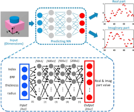
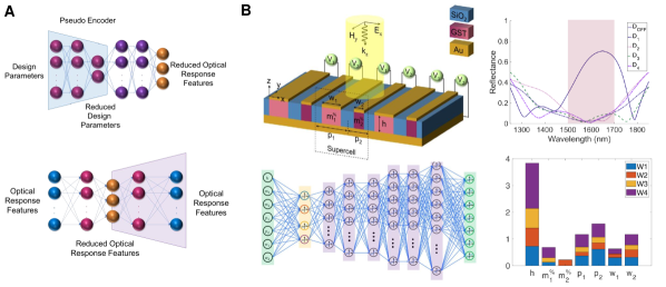
Recently, An et al. presented a deep learning-based (DL-based) technique to form a forward and inverse model for designing phase-change reconfigurable MSs An et al. (2019b). As shown in Figure 20, this method utilizes a deep neural network (DNN) to relate design and response spaces. To avoid the adverse effects of the potential abrupt changes in the phase or amplitude response of the MS in the training process, the authors wisely decompose the optical response in real and imaginary parts, which grant the smoothness of the data and thus, a more realistic trained model. As a result, the reported approach in Ref. An et al. (2019b) meaningfully accelerates the design of MSs compared to the conventional optimization approaches. Nevertheless, the efficiency of these techniques deteriorates as the number of design parameters (dimensionality of input space) and the response features (dimensionality of output space) increase. Generally, optimization algorithms suffer from high dimensionality of the input data. Therefore, it is of great importance to reduce the dimensionality of the data in the design of functional MSs.
The field of machine learning (ML) has seen extensive progress in the development of dimensionality-reduction (DR) techniques that aim to facilitate classification, data visualization, or to reduce the computational cost. Principal component analysis (PCA) is one of the most used and simple DR methods Schölkopf et al. (1997). By projecting data points on the direction of the maximum variance, this linear method finds the best approximation of the data in the reduced-dimension space. On the other hand, nonlinear DR methods like kernel PCA Mika et al. (1999), autoencoder Hinton and Salakhutdinov (2006a), etc. can potentially provide a better approximation of the data Perraul-Joncas and Meila (2013); Hinton and Salakhutdinov (2006b).
Recently, Kiarashinejad et al. Kiarashinejad et al. (2019a) developed a resolution to the existing challenges in both knowledge discovery and the design/optimization of the phase-change reconfigurable MSs by: 1) extensively reducing the dimensionality of the problem using ML-based and DL-based approaches, and 2) using the unique features of NNs for the analysis and design/optimization of the problem in the reduced dimensionality space. The resulting design tool can take a-priori information to enhance any desired feature (e.g., insensitivity to fabrication imperfections) throughout the process. It also provides a trade-off between the accepted error and the complexity (and time) of the simulations. Thus, it can be used for obtaining quick information about the role of design parameters on the overall device performance, getting detailed information about a specific feature of the device, or designing an optimal device for any given functionality. In addition, the technique in Ref. Kiarashinejad et al. (2019a) is not problem-specific, i.e., once it is trained for a given class of MSs, it can be used to design structures with a wide range of functionalities. The schematic of this method is shown in Figure 21A. First, an autoencoder (Figure 21A (top panel)) is trained to reduce the dimensionality of the response space. After that, a feed forward NN (Figure 21A (bottom panel)) is trained to model the relation between the design space and the reduced response space while reducing the dimensionality of the design space. This network, which is known as the pseudo-encoder, can predict the responses in the reduced response space given an unseen set of design parameters. The bottleneck (i.e., the NN layer with the minimum number of neurons) of the pseudo-encoder represents the reduced design space. Thanks to removing the redundancy in the data using the DR in both the design space and the response space, the relation between the reduced design space and the reduced response space can be considered as a one-to-one relation, and one can analytically solve the inverse problem. By solving the inverse problem, the reduced design parameters for a given desired response are found. Since the relation between the reduced design space and the original design space is not one-to-one, the last step of the optimization (i.e., finding the actual design parameters of the original design space) can be performed using other appropriate techniques. Kiarashinejad et al. showed that a feed forward NN modeling the relation between the original design space and the reduced design space can be used to facilitate the exhaustive search of the original design space to find the set of optimal design. This approach is a major advancement in the field as it solves the major problem in NN-based approaches for solving the non-one-to-one MS design problems.
In a following work, Kiarashinejad et al. showed that their approach can also provide valuable insights about the underlying physics of light-matter interaction in MSs Kiarashinejad et al. (2019b). The authors used their technique to assess the roles of different design parameters on the response of phase-change reconfigurable MSs. This knowledge was then used to provide better designs for the same MS functionality.
Figure 21B (left-top panel) shows the schematic of a reconfigurable MS formed by an array of nanostripes of GST, SiO2, and Au nanostripes on top of a blanket Au back reflector. The unit cell of the structure has 10 design parameters (7 geometrical design parameters and 3 GST crystalline states or equivalently indices of refraction). The response of the structure is its far-field reflection spectrum that is sampled uniformly at 200 points in the 400-800 nm wavelength range. This constitutes a 10200 dimensional problem. Using the new techniques in Ref. Kiarashinejad et al. (2019b), this problem can be reduced to a 510 dimensional space with less than 0.01 error using only 5000 simulations of the random structures to train the autoencoder and pseudo-encoder in Figure 21A Kiarashinejad et al. (2019b). Figure 21B (right-top panel) shows the response of a MS designed as a band-stop reflective filter. Figure 21B (left-bottom panel) shows a simple single-layer pseudo-encoder trained for the same structure (Figure 21B (left-top panel)) for knowledge discovery using the weights of the first (leftmost) layer of the NN. Figure 21B (right-bottom panel) shows the weights in the first layer. It clearly shows that the height of the structure is the most important design parameter while the indices of refraction of the GST nanostripes have lower importance. Indeed, these parameters have only non-negligible weights in relating to one node of the bottleneck layer in Figure 21B (left-bottom panel). In other words, the three design parameters effectively act as one design parameter. Thus, the MS can be considerably simplified by using a blanket GST layer for reconfiguration.
VII Perspective and Outlook
Despite the impressive achievements of tunable nanophotonics with phase-change chalcogenide materials, which we outlined in this review, we anticipate further growth of interest in this topic. In this subsection, we describe our vision of further research and perspectives in this actively growing area.
First of all, PCMs will continue playing a critical role in actively tunable functional MSs. As we discussed above, MSs have found many applications from microwave to optical frequencies including ultra-thin lenses, imaging, optical information processing, nonlinear optics, analog computation, and invisibility cloak Holloway et al. (2012); Zhao et al. (2014); Krasnok et al. (2018a). Changing the direction in which an input electromagnetic wave is traveling is one of the most interesting features that MSs offer. In the past few years, gradient MSs have been extensively used to steer the direction of an incident wave in reflection and/or transmission. Although this class of MSs offers unprecedented possibilities to manipulate the direction of the wave flow, they still face challenges that limit their functionalities. Gradient metal MSs are mostly designed based on the generalized law of reflection and refraction Yu et al. (2011) suffer from low efficiencies Ra’di et al. (2017); Asadchy et al. (2016). The reason is twofold: high material losses of traditional (metallic) meta-atoms and low deflection efficiency arising from the fact that this approach does not take into account the impedance mismatch between the input and desired output waves. Moreover, most of the proposed fabrication techniques result in gradient MSs with static functionalities. In other words, once a MS is fabricated based on these methods its functionality is fixed and cannot be changed.
Recently, the implementation of gradient optical MSs based on high-index dielectrics causes a high interest because of their low optical loss and novel regimes of light-matter interaction Baryshnikova et al. (2018); Staude and Schilling (2017); Kuznetsov et al. (2016); Krasnok et al. (2018b). PCMs are dielectrics and semiconductors with relatively high refractive index, and therefore, the optical response of PCM nanoparticles is governed by Mie resonances Tian et al. (2019), exhibiting lower dissipation losses especially in near-IR and mid-IR. As we have discussed in previous sections, the ability of PCMs in active tuning along with their relatively weak optical loss makes them very attractive for various gradient MSs-based tunable photonic devices including reflectors Chu et al. (2016), filters Dong et al. (2018), polarizers Zhu et al. (2018), and holograms Wan et al. (2017). We envision further growing of research works on this topic in the near future.
It has been recently shown that the issue of low deflection efficiency of gradient MSs can be overcome with the new approach to the MSs design based on the concept of metagratings Ra’di et al. (2017). Metagratings are periodic arrays of polarizable particles where the period is comparable to the wavelength. When such a structure is illuminated with an incident wave, in addition to possible scattering into the specular directions, other Floquet modes can, in principle, carry energy away from the surface. Depending on the angle in which the incident wave is illuminating the surface and also the periodicity of the metagrating, the different number of propagating Floquet modes can be present. The direction of these Floquet modes can be controlled by the periodicity of the structure making such surfaces a rich platform for efficient manipulation of electromagnetic waves. MSs designed based on this approach can reroute the incident wave to the desired direction with 100% efficiency. Also, MSs designed based on this method do not require subwavelength structures lifting fabrication challenges faced by conventional gradient MSs. The use of reversible PCMs would make it possible to erase and rewrite the pattern on the PCM surfaces to achieve the metagrating operation that can be used for controlling electromagnetic waves in a wide range of wavelengths and frequencies. An integration of this platform with a 2D pulse shaper can be used to imprint the designed pattern on the chosen substrate materials, as it has been done for zone-plate devices in Ref. Wang et al. (2016) or for polariton nanophotonics in Ref. Chaudhary et al. (2019).
Recent studies in light scattering engineering made it feasible to tailor structures with unique scattering properties. One of such unusual scattering phenomena is the bound states in the continuum (BICs) with unboundedly large Q-factors and vanishing scattering lines in open systems, which have been recently discovered in photonics Marinica et al. (2008); Hsu et al. (2016); Monticone and Alù (2014); Monticone et al. (2018); Krasnok et al. (2019); Koshelev et al. (2018). The existence of these states allows designing optical MSs with diverging and potentially infinite lifetimes. It has been demonstrated that the use of BICs in lasers, nonlinear optics, and sensors allows significant boosting of the performance of these vital applications. Nanoparticles made of high-index dielectrics governed by Mie modes have been demonstrated to be a powerful platform for tailoring BICs-supporting nanostructures and MSs Koshelev et al. (2018); Liu et al. (2019). However, the reported devices supporting BICs are rather static, with just a few exceptions Fan et al. (2019b). We belive that BIC-supporting dielectric MSs can be made of PCMs that will make them tunable and reconfigurable significantly expanding the possibilities of their practical application.
Another example of unusual scattering phenomena that can benefit from the use of PCMs is the so-called exceptional points (EPs) arising in non-Hermitian structures Krasnok et al. (2019); Miri and Alù (2019). Exceptional points correspond to the case when pairs of eigenstates and corresponding eigenvalues of a non-Hermitian operator (e.g., Hamiltonian or S-matrix) coalesce. In structures comprising a balanced amount of gain and loss known as parity-time symmetric Krasnok et al. (2019), EPs can arise at a real frequency and hence can be detected via CW monochromatic excitation. The existence of EPs results in a nonlinear dependence of the response of a system to variation of the system’s parameters (e.g., frequency detuning, amount of loss or gain). This peculiarity makes them interesting for ultra-sensitive sensor devices, single-mode lasers and quantum optics Krasnok et al. (2019). The use of PCMs provides a fruitful approach to precise tailoring material loss in space and time and hence can facilitate the designing and realization of structures supporting EPs Huang et al. (2017) especially in the integrated on-chip scenario.
The advances of nanophotonics can facilitate the reduction of the power consumption of PCMs-based photonics structures. Usually, to take full advantage of a pronounced change of the dielectric function of PCMs, bare PCMs have to be transformed from the amorphous to the fully crystalline phase, which requires relatively strong laser fields or strong external electrical bias Tian et al. (2019); Wuttig and Yamada (2007); Alaee et al. (2016); Huang et al. (2018); Wuttig et al. (2017). For example, the full transition from crystalline to amorphous phase for bare GST material requires a peak intensity of 1 mWm-2 Němec et al. (2009). Although such intensities are not weak, they are much weaker than those used in other reversible approaches including electron-hole plasma excitation that requires laser intensities of 103 – 1055 mWm-2 Baranov et al. (2016); Makarov et al. (2015); Shcherbakov et al. (2015); Yang et al. (2015); Paniagua-Domínguez et al. (2019), and comparable with the intensity of thermo-optical nonlinearity of Si Zograf et al. (2017). As we discussed above, the power consumption and tuning intensities of PCMs-based devices can be significantly reduced via strong optical heating araising at surface plasmonic resonances of metal nanostructures Dong et al. (2018); Cao et al. (2018, 2013c).
The use of PCM in nanoantennas with several employed coupled resonant modes allows efficient tuning of their power pattern Alaee et al. (2016); Lepeshov et al. (2019b). In contrast to the spectral properties of an antenna, its scattering pattern demonstrates a stronger tunability because it relies rather on the relative phases of involved modes. For example, in paper Lepeshov et al. (2019b), a hybrid metal-semiconductor core-shell nanoantenna made of silver Ag core and phase-changing GeTe shell has been designed to possess switching between the superscattering regime and nonradiative cloaking state with remarkably low power consumption. It has been shown that tuning of the PCM crystallinity leads to a tremendous change in the total (15 times) and forward (100 times) scattering with the characteristic intensity of 10 Wm-2 which is 2 orders of magnitude weaker than for bare GeTe material or Si particles tuning by thermal heating.
To harness the disruptive concept of meta-optics in the realization of on-demand adaptive functionalities, design of dynamically reconfigurable MSs with unprecedented performance is indispensable. Although increasing the number of design parameters spans the optimization landscape (or equivalently space dimensionality) that helps electromagnetic designers find the best possible solution, this freedom adds serious complexities to the design process. While employing conventional approaches such as topology and multi-objective optimization techniques have resulted in high-performance, complicated metadevices, so far, such methods have been limited to the context of non-tunable meta-optics with predefined fixed functionalities. Newly emergent deep learning approaches as a powerful platform for intelligent analysis, design, and optimization of tunable MSs, leveraging functional materials including PCMS, can empower electromagnetic designers to effectively overcome hyper-dimensional problems with reasonable computational resources.
Integrating chalcogenide PCMs with PICs has enabled reversible switching between arbitrary states, which makes them near-ideal candidates for all-photonic implementation of switches and modulators, memories, arithmetic processors and neurosynaptic systems. However, there is still room for improvement of integrated phase-change photonic devices to outperform their electronic counterparts Wright et al. (2019). On top is the switching energy required for phase transition of the PCM. Although the switching energy falls in the range from 50 pJ to a few nJ Ríos et al. (2015); Stegmaier et al. (2017); Wu et al. (2018); Li et al. (2019), a 0.1 pJ switching energy has already been demonstrated in an electronic phase-change memory Xiong et al. (2011). Therefore, it is very crucial to develop new architectures such as plasmonic nanogaps Gemo et al. (2019); Farmakidis et al. (2019), photonic crystal cavities von Keitz et al. (2018) and crossing waveguides Zhang et al. (2019c, b) offering hotspots in which the PCM elements could be exposed to an enhanced electromagnetic field to reduce the required transformation energy. Another aspect is the switching speed. While several types of triggering optical/electical pulses (single pulses with tens of ns widths, or groups of ps pulses) have been used for stepwise crystallization of the PCM element, the finite crystallization time of PCMs has limited the switching speed Loke et al. (2012). To improve this, pulse shape engineering is necessary. Recently, a qualitative study on the origin and mechanism of the phase switching in the PCMs has been reported in Ref. Rios et al. (2018) to describe the switching dynamics for precise control during amorphization and crytallization. The third area for improvement is the maximum number of cycles that a PCM cell can be switched between states, or the durability of the switching process. An endurance of more than cycles has been reported for electronic phase-change memories Kuzum et al. (2011). Therefore, for the realization of all-photonic ultrafast processing applications, a higher number of cycles is needed. To do so, one may use some new materials development approaches reported in Refs. Salinga et al. (2018); Zhang and Ma (2018).
Acknowledgment: This work was supported by Office of Naval Research (ONR)(N00014-18-1-2055, Dr. B. Bennett).
Conflict of interest: The authors declare no competing financial interest.
References
- Sun et al. (2015) C. Sun, M. T. Wade, Y. Lee, J. S. Orcutt, L. Alloatti, M. S. Georgas, A. S. Waterman, J. M. Shainline, R. R. Avizienis, S. Lin, et al., Single-chip microprocessor that communicates directly using light, Nature 528, 534 (2015).
- Atabaki et al. (2018) A. H. Atabaki, S. Moazeni, F. Pavanello, H. Gevorgyan, J. Notaros, L. Alloatti, M. T. Wade, C. Sun, S. A. Kruger, H. Meng, et al., Integrating photonics with silicon nanoelectronics for the next generation of systems on a chip, Nature 556, 349 (2018).
- Zeng et al. (2014) W. Zeng, L. Shu, Q. Li, S. Chen, F. Wang, and X.-M. Tao, Fiber-based wearable electronics: a review of materials, fabrication, devices, and applications, Advanced materials 26, 5310 (2014).
- Rickman (2014) A. Rickman, The commercialization of silicon photonics, Nature Photonics 8, 579 (2014).
- Thomson et al. (2016) D. Thomson, A. Zilkie, J. E. Bowers, T. Komljenovic, G. T. Reed, L. Vivien, D. Marris-Morini, E. Cassan, L. Virot, J.-M. Fédéli, et al., Roadmap on silicon photonics, Journal of Optics 18, 073003 (2016).
- Genevet et al. (2017) P. Genevet, F. Capasso, F. Aieta, M. Khorasaninejad, and R. Devlin, Recent advances in planar optics: from plasmonic to dielectric metasurfaces, Optica 4, 139 (2017).
- Yu et al. (2011) N. Yu, P. Genevet, M. A. Kats, F. Aieta, J.-P. Tetienne, F. Capasso, and Z. Gaburro, Light propagation with phase discontinuities: generalized laws of reflection and refraction, science , 1210713 (2011).
- Staude et al. (2013) I. Staude, A. E. Miroshnichenko, M. Decker, N. T. Fofang, S. Liu, E. Gonzales, J. Dominguez, T. S. Luk, D. N. Neshev, I. Brener, et al., Tailoring directional scattering through magnetic and electric resonances in subwavelength silicon nanodisks, ACS nano 7, 7824 (2013).
- Arbabi et al. (2015) A. Arbabi, Y. Horie, M. Bagheri, and A. Faraon, Dielectric metasurfaces for complete control of phase and polarization with subwavelength spatial resolution and high transmission, Nature nanotechnology 10, 937 (2015).
- Khorasaninejad et al. (2016) M. Khorasaninejad, W. T. Chen, R. C. Devlin, J. Oh, A. Y. Zhu, and F. Capasso, Metalenses at visible wavelengths: Diffraction-limited focusing and subwavelength resolution imaging, Science 352, 1190 (2016).
- Ding et al. (2018a) F. Ding, R. Deshpande, and S. I. Bozhevolnyi, Bifunctional gap-plasmon metasurfaces for visible light: polarization-controlled unidirectional surface plasmon excitation and beam steering at normal incidence, Light: Science & Applications 7, 17178 (2018a).
- Yesilkoy et al. (2019) F. Yesilkoy, E. R. Arvelo, Y. Jahani, M. Liu, A. Tittl, V. Cevher, Y. Kivshar, and H. Altug, Ultrasensitive hyperspectral imaging and biodetection enabled by dielectric metasurfaces, Nature Photonics 13, 390 (2019).
- Arbabi et al. (2016) E. Arbabi, A. Arbabi, S. M. Kamali, Y. Horie, and A. Faraon, Multiwavelength polarization-insensitive lenses based on dielectric metasurfaces with meta-molecules, Optica 3, 628 (2016).
- Arbabi et al. (2018a) E. Arbabi, S. M. Kamali, A. Arbabi, and A. Faraon, Full-stokes imaging polarimetry using dielectric metasurfaces, ACS Photonics 5, 3132 (2018a).
- Lee et al. (2018) G.-Y. Lee, G. Yoon, S.-Y. Lee, H. Yun, J. Cho, K. Lee, H. Kim, J. Rho, and B. Lee, Complete amplitude and phase control of light using broadband holographic metasurfaces, Nanoscale 10, 4237 (2018).
- Ha et al. (2018) S. T. Ha, Y. H. Fu, N. K. Emani, Z. Pan, R. M. Bakker, R. Paniagua-Domínguez, and A. I. Kuznetsov, Directional lasing in resonant semiconductor nanoantenna arrays, Nature nanotechnology 13, 1042 (2018).
- Abdollahramezani et al. (2017) S. Abdollahramezani, A. Chizari, A. E. Dorche, M. V. Jamali, and J. A. Salehi, Dielectric metasurfaces solve differential and integro-differential equations, Optics letters 42, 1197 (2017).
- Tran et al. (2017) T. T. Tran, D. Wang, Z.-Q. Xu, A. Yang, M. Toth, T. W. Odom, and I. Aharonovich, Deterministic coupling of quantum emitters in 2d materials to plasmonic nanocavity arrays, Nano letters 17, 2634 (2017).
- Krasnok et al. (2018a) A. Krasnok, M. Tymchenko, and A. Alu, Nonlinear metasurfaces: a paradigm shift in nonlinear optics, Materials Today 21, 8 (2018a).
- Hemmatyar et al. (2019) O. Hemmatyar, S. Abdollahramezani, Y. Kiarashinejad, M. Zandehshahvar, and A. Adibi, Full color generation with fano-type resonant hfo2 nanopillars designed by a deep-learning approach, Nanoscale 11, 21266 (2019).
- Krasnok et al. (2018b) A. Krasnok, M. Caldarola, N. Bonod, and A. Alú, Spectroscopy and biosensing with optically resonant dielectric nanostructures, Advanced Optical Materials 6 (2018b).
- Jahani and Jacob (2016) S. Jahani and Z. Jacob, All-dielectric metamaterials, Nature nanotechnology 11, 23 (2016).
- Kuznetsov et al. (2016) A. I. Kuznetsov, A. E. Miroshnichenko, M. L. Brongersma, Y. S. Kivshar, and B. Luk’yanchuk, Optically resonant dielectric nanostructures, Science 354, aag2472 (2016).
- Baranov et al. (2017) D. G. Baranov, D. A. Zuev, S. I. Lepeshov, O. V. Kotov, A. E. Krasnok, A. B. Evlyukhin, and B. N. Chichkov, All-dielectric nanophotonics: the quest for better materials and fabrication techniques, Optica 4, 814 (2017).
- Staude and Schilling (2017) I. Staude and J. Schilling, Metamaterial-inspired silicon nanophotonics, Nature Photonics 11, 274 (2017).
- Ding et al. (2017) F. Ding, A. Pors, and S. I. Bozhevolnyi, Gradient metasurfaces: a review of fundamentals and applications, Reports on Progress in Physics 81, 026401 (2017).
- Su et al. (2018) V.-C. Su, C. H. Chu, G. Sun, and D. P. Tsai, Advances in optical metasurfaces: fabrication and applications, Optics express 26, 13148 (2018).
- Ding et al. (2018b) F. Ding, Y. Yang, R. A. Deshpande, and S. I. Bozhevolnyi, A review of gap-surface plasmon metasurfaces: fundamentals and applications, Nanophotonics 7, 1129 (2018b).
- Kamali et al. (2018) S. M. Kamali, E. Arbabi, A. Arbabi, and A. Faraon, A review of dielectric optical metasurfaces for wavefront control, Nanophotonics 7, 1041 (2018).
- Neshev and Aharonovich (2018) D. Neshev and I. Aharonovich, Optical metasurfaces: new generation building blocks for multi-functional optics, Light: Science & Applications 7, 1 (2018).
- Tseng et al. (2018) M. L. Tseng, H.-H. Hsiao, C. H. Chu, M. K. Chen, G. Sun, A.-Q. Liu, and D. P. Tsai, Metalenses: advances and applications, Advanced Optical Materials 6, 1800554 (2018).
- Luo (2018) X. Luo, Subwavelength optical engineering with metasurface waves, Advanced Optical Materials 6, 1701201 (2018).
- He et al. (2018) Q. He, S. Sun, S. Xiao, and L. Zhou, High-efficiency metasurfaces: Principles, realizations, and applications, Advanced Optical Materials 6, 1800415 (2018).
- Wen et al. (2018a) D. Wen, F. Yue, W. Liu, S. Chen, and X. Chen, Geometric metasurfaces for ultrathin optical devices, Advanced Optical Materials 6, 1800348 (2018a).
- Chen et al. (2019) S. Chen, W. Liu, Z. Li, H. Cheng, and J. Tian, Metasurface-empowered optical multiplexing and multifunction, Advanced Materials (2019).
- Zang et al. (2019) W. Zang, Q. Yuan, R. Chen, L. Li, T. Li, X. Zou, G. Zheng, Z. Chen, S. Wang, Z. Wang, et al., Chromatic dispersion manipulation based on metalenses, Advanced Materials (2019).
- Staude et al. (2019) I. Staude, T. Pertsch, and Y. S. Kivshar, All-dielectric resonant meta-optics lightens up, ACS Photonics 6, 802 (2019).
- (38) J. Sung, G.-Y. Lee, and B. Lee, Progresses in the practical metasurface for holography and lens, Nanophotonics 8, 1701.
- Vaskin et al. (2019) A. Vaskin, R. Kolkowski, A. F. Koenderink, and I. Staude, Light-emitting metasurfaces, Nanophotonics 8, 1151 (2019).
- (40) S. Chen, Y. Zhang, Z. Li, H. Cheng, and J. Tian, Empowered layer effects and prominent properties in few-layer metasurfaces, Advanced Optical Materials , 1801477.
- (41) K. Koshelev, G. Favraud, A. Bogdanov, Y. Kivshar, and A. Fratalocchi, Nonradiating photonics with resonant dielectric nanostructures, Nanophotonics 8, 725.
- Fan et al. (2019a) R.-H. Fan, B. Xiong, R.-W. Peng, and M. Wang, Constructing metastructures with broadband electromagnetic functionality, Advanced Materials (2019a).
- Zhuang et al. (2015) L. Zhuang, C. G. Roeloffzen, M. Hoekman, K.-J. Boller, and A. J. Lowery, Programmable photonic signal processor chip for radiofrequency applications, Optica 2, 854 (2015).
- Capmany et al. (2016) J. Capmany, I. Gasulla, and D. Pérez, Microwave photonics: The programmable processor, Nature Photonics 10, 6 (2016).
- Harris et al. (2017) N. C. Harris, G. R. Steinbrecher, M. Prabhu, Y. Lahini, J. Mower, D. Bunandar, C. Chen, F. N. Wong, T. Baehr-Jones, M. Hochberg, et al., Quantum transport simulations in a programmable nanophotonic processor, Nature Photonics 11, 447 (2017).
- Pérez et al. (2017) D. Pérez, I. Gasulla, L. Crudgington, D. J. Thomson, A. Z. Khokhar, K. Li, W. Cao, G. Z. Mashanovich, and J. Capmany, Multipurpose silicon photonics signal processor core, Nature communications 8, 636 (2017).
- Shen et al. (2017) Y. Shen, N. C. Harris, S. Skirlo, M. Prabhu, T. Baehr-Jones, M. Hochberg, X. Sun, S. Zhao, H. Larochelle, D. Englund, et al., Deep learning with coherent nanophotonic circuits, Nature Photonics 11, 441 (2017).
- Tait et al. (2017) A. N. Tait, T. F. De Lima, E. Zhou, A. X. Wu, M. A. Nahmias, B. J. Shastri, and P. R. Prucnal, Neuromorphic photonic networks using silicon photonic weight banks, Scientific reports 7, 7430 (2017).
- Wang et al. (2018) J. Wang, S. Paesani, Y. Ding, R. Santagati, P. Skrzypczyk, A. Salavrakos, J. Tura, R. Augusiak, L. Mančinska, D. Bacco, et al., Multidimensional quantum entanglement with large-scale integrated optics, Science 360, 285 (2018).
- Kim et al. (2019) J.-H. Kim, S. Aghaeimeibodi, J. Carolan, D. Englund, and E. Waks, Hybrid integration methods for on-chip quantum photonics, arXiv preprint arXiv:1911.12756 (2019).
- Sherrott et al. (2017) M. C. Sherrott, P. W. Hon, K. T. Fountaine, J. C. Garcia, S. M. Ponti, V. W. Brar, L. A. Sweatlock, and H. A. Atwater, Experimental demonstration of¿ 230 phase modulation in gate-tunable graphene–gold reconfigurable mid-infrared metasurfaces, Nano letters 17, 3027 (2017).
- Lewi et al. (2015) T. Lewi, P. P. Iyer, N. A. Butakov, A. A. Mikhailovsky, and J. A. Schuller, Widely tunable infrared antennas using free carrier refraction, Nano letters 15, 8188 (2015).
- Kafaie Shirmanesh et al. (2018) G. Kafaie Shirmanesh, R. Sokhoyan, R. A. Pala, and H. A. Atwater, Dual-gated active metasurface at 1550 nm with wide (¿ 300∘) phase tunability, Nano letters 18, 2957 (2018).
- (54) Y. Kim, P. C. Wu, R. Sokhoyan, K. A. Mauser, R. Glaudell, G. Kafaie Shirmanesh, and H. A. Atwater, Phase modulation with electrically tunable vanadium dioxide phase-change metasurfaces, Nano letters .
- Palm et al. (2018) K. J. Palm, J. B. Murray, T. C. Narayan, and J. N. Munday, Dynamic optical properties of metal hydrides, ACS Photonics 5, 4677 (2018).
- Komar et al. (2017) A. Komar, Z. Fang, J. Bohn, J. Sautter, M. Decker, A. Miroshnichenko, T. Pertsch, I. Brener, Y. S. Kivshar, I. Staude, et al., Electrically tunable all-dielectric optical metasurfaces based on liquid crystals, Applied Physics Letters 110, 071109 (2017).
- Arbabi et al. (2018b) E. Arbabi, A. Arbabi, S. M. Kamali, Y. Horie, M. Faraji-Dana, and A. Faraon, Mems-tunable dielectric metasurface lens, Nature communications 9, 812 (2018b).
- Kamali et al. (2016) S. M. Kamali, E. Arbabi, A. Arbabi, Y. Horie, and A. Faraon, Highly tunable elastic dielectric metasurface lenses, Laser & Photonics Reviews 10, 1002 (2016).
- Zuev et al. (2016) D. A. Zuev, S. V. Makarov, I. S. Mukhin, V. A. Milichko, S. V. Starikov, I. A. Morozov, I. I. Shishkin, A. E. Krasnok, and P. A. Belov, Fabrication of hybrid nanostructures via nanoscale laser-induced reshaping for advanced light manipulation, Advanced Materials 28, 3087 (2016).
- Taghinejad et al. (2018) M. Taghinejad, H. Taghinejad, Z. Xu, K.-T. Lee, S. P. Rodrigues, J. Yan, A. Adibi, T. Lian, and W. Cai, Ultrafast control of phase and polarization of light expedited by hot-electron transfer, Nano letters 18, 5544 (2018).
- Lepeshov et al. (2019a) S. I. Lepeshov, A. E. Krasnok, P. A. Belov, and A. E. Miroshnichenko, Hybrid nanophotonics, Physics-Uspekhi 61, 1035 (2019a).
- Koos et al. (2009) C. Koos, P. Vorreau, T. Vallaitis, P. Dumon, W. Bogaerts, R. Baets, B. Esembeson, I. Biaggio, T. Michinobu, F. Diederich, et al., All-optical high-speed signal processing with silicon–organic hybrid slot waveguides, Nature photonics 3, 216 (2009).
- Phare et al. (2015) C. T. Phare, Y.-H. D. Lee, J. Cardenas, and M. Lipson, Graphene electro-optic modulator with 30 ghz bandwidth, Nature Photonics 9, 511 (2015).
- Markov et al. (2015) P. Markov, R. E. Marvel, H. J. Conley, K. J. Miller, R. F. Haglund Jr, and S. M. Weiss, Optically monitored electrical switching in vo2, Acs Photonics 2, 1175 (2015).
- Haffner et al. (2015) C. Haffner, W. Heni, Y. Fedoryshyn, J. Niegemann, A. Melikyan, D. L. Elder, B. Bäuerle, Y. Salamin, A. Josten, U. Koch, et al., All-plasmonic mach–zehnder modulator enabling optical high-speed communication at the microscale, Nature Photonics 9, 525 (2015).
- Feng et al. (2012) D. Feng, S. Liao, H. Liang, J. Fong, B. Bijlani, R. Shafiiha, B. J. Luff, Y. Luo, J. Cunningham, A. V. Krishnamoorthy, et al., High speed gesi electro-absorption modulator at 1550 nm wavelength on soi waveguide, Optics express 20, 22224 (2012).
- Behera et al. (2017) J. K. Behera, X. Zhou, J. Tominaga, and R. E. Simpson, Laser switching and characterisation of chalcogenides: systems, measurements, and applicability to photonics, Optical Materials Express 7, 3741 (2017).
- Raeis-Hosseini and Rho (2017) N. Raeis-Hosseini and J. Rho, Metasurfaces based on phase-change material as a reconfigurable platform for multifunctional devices, Materials 10, 1046 (2017).
- Ferrera et al. (2017) M. Ferrera, N. Kinsey, A. Shaltout, C. DeVault, V. Shalaev, and A. Boltasseva, Dynamic nanophotonics, JOSA B 34, 95 (2017).
- Wuttig et al. (2017) M. Wuttig, H. Bhaskaran, and T. Taubner, Phase-change materials for non-volatile photonic applications, Nature Photonics 11, 465 (2017).
- Miller et al. (2018) K. J. Miller, R. F. Haglund, and S. M. Weiss, Optical phase change materials in integrated silicon photonic devices, Optical Materials Express 8, 2415 (2018).
- Bang et al. (2018) S. Bang, J. Kim, G. Yoon, T. Tanaka, and J. Rho, Recent advances in tunable and reconfigurable metamaterials, Micromachines 9, 560 (2018).
- Nemati et al. (2018) A. Nemati, Q. Wang, M. Hong, and J. Teng, Tunable and reconfigurable metasurfaces and metadevices, Opto-Electronic Advances 1, 180009 (2018).
- Krasnok and Alù (2019) A. Krasnok and A. Alù, Active nanophotonics, arXiv preprint arXiv:1912.03801 (2019).
- (75) C. U. Hail, A.-K. U. Michel, D. Poulikakos, and H. Eghlidi, Optical metasurfaces: Evolving from passive to adaptive, Advanced Optical Materials , 1801786.
- Paniagua-Domínguez et al. (2019) R. Paniagua-Domínguez, S. T. Ha, and A. I. Kuznetsov, Active and tunable nanophotonics with dielectric nanoantennas, Proceedings of the IEEE (2019).
- Cao and Cen (2019) T. Cao and M. Cen, Fundamentals and applications of chalcogenide phase-change material photonics, Advanced Theory and Simulations 2, 1900094 (2019).
- Cui et al. (2019) T. Cui, B. Bai, and H.-B. Sun, Tunable metasurfaces based on active materials, Advanced Functional Materials 29, 1806692 (2019).
- Zou et al. (2019) C. Zou, J. Sautter, F. Setzpfandt, and I. Staude, Resonant dielectric metasurfaces: active tuning and nonlinear effects, Journal of Physics D: Applied Physics 52, 373002 (2019).
- He et al. (2019) Q. He, S. Sun, L. Zhou, et al., Tunable/reconfigurable metasurfaces: Physics and applications, Research 2019, 1849272 (2019).
- Taghinejad and Cai (2019) M. Taghinejad and W. Cai, All-optical control of light in micro-and nanophotonics, ACS Photonics 6, 1082 (2019).
- (82) F. Ding, Y. Yang, and S. I. Bozhevolnyi, Dynamic metasurfaces using phase-change chalcogenides, Advanced Optical Materials , 1801709.
- Shaltout et al. (2019) A. M. Shaltout, V. M. Shalaev, and M. L. Brongersma, Spatiotemporal light control with active metasurfaces, Science 364, eaat3100 (2019).
- (84) L. Kang, R. P. Jenkins, and D. H. Werner, Recent progress in active optical metasurfaces, Advanced Optical Materials , 1801813.
- (85) D. Pérez, I. Gasulla, and J. Capmany, Programmable multifunctional integrated nanophotonics, Nanophotonics 7, 1351.
- Harris et al. (2018) N. C. Harris, J. Carolan, D. Bunandar, M. Prabhu, M. Hochberg, T. Baehr-Jones, M. L. Fanto, A. M. Smith, C. C. Tison, P. M. Alsing, et al., Linear programmable nanophotonic processors, Optica 5, 1623 (2018).
- Wright et al. (2019) C. D. Wright, H. Bhaskaran, and W. H. Pernice, Integrated phase-change photonic devices and systems, MRS Bulletin 44, 721 (2019).
- Ovshinsky (1968) S. R. Ovshinsky, Reversible electrical switching phenomena in disordered structures, Physical Review Letters 21, 1450 (1968).
- Hajto et al. (1994) J. Hajto, A. Snell, J. Hu, A. Holmes, A. Owen, M. Rose, and R. Gibson, Metal-semiconductor transition in electroformed chromium/amorphous silicon/vanadium thin-film structures, Philosophical Magazine B 69, 237 (1994).
- Argall (1968) F. Argall, Switching phenomena in titanium oxide thin films, Solid-State Electronics 11, 535 (1968).
- Owen and Robertson (1973) A. E. Owen and J. M. Robertson, Electronic conduction and switching in chalcogenide glasses, IEEE transactions on electron devices 20, 105 (1973).
- Wuttig (2005) M. Wuttig, Phase-change materials: Towards a universal memory?, Nature materials 4, 265 (2005).
- Meinders et al. (2006) E. R. Meinders, A. V. Mijiritskii, L. Van Pieterson, and M. Wuttig, Optical Data Storage: Phase-change media and recording, Vol. 4 (Springer Science & Business Media, 2006).
- Yamada et al. (1987) N. Yamada, E. Ohno, N. Akahira, K. Nishiuchi, K. Nagata, and M. Takao, High speed overwritable phase change optical disk material, Japanese Journal of Applied Physics 26, 61 (1987).
- Neale and Aseltine (1973) R. Neale and J. A. Aseltine, The application of amorphous materials to computer memories, IEEE Transactions on Electron Devices 20, 195 (1973).
- Chen et al. (1986) M. Chen, K. A. Rubin, and R. Barton, Compound materials for reversible, phase-change optical data storage, Applied physics letters 49, 502 (1986).
- Yamada et al. (1991) N. Yamada, E. Ohno, K. Nishiuchi, N. Akahira, and M. Takao, Rapid-phase transitions of gete-sb2te3 pseudobinary amorphous thin films for an optical disk memory, Journal of Applied Physics 69, 2849 (1991).
- Coombs et al. (1995) J. Coombs, A. Jongenelis, W. van Es-Spiekman, and B. Jacobs, Laser-induced crystallization phenomena in gete-based alloys. i. characterization of nucleation and growth, Journal of applied physics 78, 4906 (1995).
- Yamada and Matsunaga (2000) N. Yamada and T. Matsunaga, Structure of laser-crystallized ge 2 sb 2+ x te 5 sputtered thin films for use in optical memory, Journal of Applied Physics 88, 7020 (2000).
- Wełnic et al. (2006) W. Wełnic, A. Pamungkas, R. Detemple, C. Steimer, S. Blügel, and M. Wuttig, Unravelling the interplay of local structure and physical properties in phase-change materials, Nature Materials 5, 56 (2006).
- Nonaka et al. (2000) T. Nonaka, G. Ohbayashi, Y. Toriumi, Y. Mori, and H. Hashimoto, Crystal structure of gete and ge2sb2te5 meta-stable phase, Thin Solid Films 370, 258 (2000).
- Friedrich et al. (2000) I. Friedrich, V. Weidenhof, W. Njoroge, P. Franz, and M. Wuttig, Structural transformations of ge2sb2te5 films studied by electrical resistance measurements, Journal of Applied Physics 87, 4130 (2000).
- Kolobov et al. (2004) A. V. Kolobov, P. Fons, A. I. Frenkel, A. L. Ankudinov, J. Tominaga, and T. Uruga, Understanding the phase-change mechanism of rewritable optical media, Nature materials 3, 703 (2004).
- Friedrich et al. (2001) I. Friedrich, V. Weidenhof, S. Lenk, and M. Wuttig, Morphology and structure of laser-modified ge2sb2te5 films studied by transmission electron microscopy, Thin solid films 389, 239 (2001).
- Kalb et al. (2005) J. Kalb, F. Spaepen, and M. Wuttig, Kinetics of crystal nucleation in undercooled droplets of sb-and te-based alloys used for phase change recording, Journal of applied Physics 98, 054910 (2005).
- Zhang et al. (2019a) Y. Zhang, J. B. Chou, J. Li, H. Li, Q. Du, A. Yadav, S. Zhou, M. Y. Shalaginov, Z. Fang, H. Zhong, et al., Broadband transparent optical phase change materials for high-performance nonvolatile photonics, Nature communications 10, 1 (2019a).
- Njoroge et al. (2002) W. K. Njoroge, H.-W. Wöltgens, and M. Wuttig, Density changes upon crystallization of ge 2 sb 2.04 te 4.74 films, Journal of Vacuum Science & Technology A: Vacuum, Surfaces, and Films 20, 230 (2002).
- Wełnic et al. (2007) W. Wełnic, S. Botti, L. Reining, and M. Wuttig, Origin of the optical contrast in phase-change materials, Physical review letters 98, 236403 (2007).
- Yamada et al. (2002) N. Yamada, R. Kojima, M. Uno, T. Akiyama, H. Kitaura, K. Narumi, and K. Nishiuchi, Phase-change material for use in rewritable dual-layer optical disk, in Optical Data Storage 2001, Vol. 4342 (International Society for Optics and Photonics, 2002) pp. 55–63.
- Privitera et al. (2003) S. Privitera, E. Rimini, C. Bongiorno, R. Zonca, A. Pirovano, and R. Bez, Crystallization and phase separation in ge 2+ x sb 2 te 5 thin films, Journal of applied physics 94, 4409 (2003).
- Zhang et al. (2018a) Q. Zhang, Y. Zhang, J. Li, R. Soref, T. Gu, and J. Hu, Broadband nonvolatile photonic switching based on optical phase change materials: beyond the classical figure-of-merit, Optics letters 43, 94 (2018a).
- Dong et al. (2019) W. Dong, H. Liu, J. K. Behera, L. Lu, R. J. Ng, K. V. Sreekanth, X. Zhou, J. K. Yang, and R. E. Simpson, Wide bandgap phase change material tuned visible photonics, Advanced Functional Materials 29, 1806181 (2019).
- Luo and Wuttig (2004) M. Luo and M. Wuttig, The dependence of crystal structure of te-based phase-change materials on the number of valence electrons, Advanced Materials 16, 439 (2004).
- Lu et al. (2019) L. Lu, W. Dong, J. K. Behera, L. Chew, and R. E. Simpson, Inter-diffusion of plasmonic metals and phase change materials, Journal of materials science 54, 2814 (2019).
- Sámson et al. (2010) Z. Sámson, K. MacDonald, F. De Angelis, B. Gholipour, K. Knight, C. Huang, E. Di Fabrizio, D. Hewak, and N. Zheludev, Metamaterial electro-optic switch of nanoscale thickness, Applied Physics Letters 96, 143105 (2010).
- Gholipour et al. (2013) B. Gholipour, J. Zhang, K. F. MacDonald, D. W. Hewak, and N. I. Zheludev, An all-optical, non-volatile, bidirectional, phase-change meta-switch, Advanced materials 25, 3050 (2013).
- Chen et al. (2013) Y. Chen, T. Kao, B. Ng, X. Li, X. Luo, B. Luk’Yanchuk, S. Maier, and M. Hong, Hybrid phase-change plasmonic crystals for active tuning of lattice resonances, Optics express 21, 13691 (2013).
- Cao et al. (2014a) T. Cao, C. Wei, R. E. Simpson, L. Zhang, and M. J. Cryan, Fast tuning of double fano resonance using a phase-change metamaterial under low power intensity, Scientific reports 4, 4463 (2014a).
- Johnson et al. (2002) S. G. Johnson, M. Ibanescu, M. Skorobogatiy, O. Weisberg, J. Joannopoulos, and Y. Fink, Perturbation theory for maxwell’s equations with shifting material boundaries, Physical review E 65, 066611 (2002).
- Cao et al. (2014b) T. Cao, C.-w. Wei, R. E. Simpson, L. Zhang, and M. J. Cryan, Broadband polarization-independent perfect absorber using a phase-change metamaterial at visible frequencies, Scientific reports 4, 3955 (2014b).
- Cao et al. (2013a) T. Cao, L. Zhang, R. E. Simpson, and M. J. Cryan, Mid-infrared tunable polarization-independent perfect absorber using a phase-change metamaterial, JOSA B 30, 1580 (2013a).
- Cao et al. (2013b) T. Cao, L. Zhang, R. E. Simpson, C. Wei, and M. J. Cryan, Strongly tunable circular dichroism in gammadion chiral phase-change metamaterials, Optics express 21, 27841 (2013b).
- Rudé et al. (2016) M. Rudé, V. Mkhitaryan, A. E. Cetin, T. A. Miller, A. Carrilero, S. Wall, F. J. G. de Abajo, H. Altug, and V. Pruneri, Ultrafast and broadband tuning of resonant optical nanostructures using phase-change materials, Advanced Optical Materials 4, 1060 (2016).
- Qu et al. (2017) Y. Qu, Q. Li, K. Du, L. Cai, J. Lu, and M. Qiu, Dynamic thermal emission control based on ultrathin plasmonic metamaterials including phase-changing material gst, Laser & Photonics Reviews 11, 1700091 (2017).
- Cao et al. (2018) T. Cao, X. Zhang, W. Dong, L. Lu, X. Zhou, X. Zhuang, J. Deng, X. Cheng, G. Li, and R. E. Simpson, Tuneable thermal emission using chalcogenide metasurface, Advanced Optical Materials 6, 1800169 (2018).
- Carrillo et al. (2016) S. G.-C. Carrillo, G. R. Nash, H. Hayat, M. J. Cryan, M. Klemm, H. Bhaskaran, and C. D. Wright, Design of practicable phase-change metadevices for near-infrared absorber and modulator applications, Optics express 24, 13563 (2016).
- Carrillo et al. (2018) S. G.-C. Carrillo, A. M. Alexeev, Y.-Y. Au, and C. D. Wright, Reconfigurable phase-change meta-absorbers with on-demand quality factor control, Optics express 26, 25567 (2018).
- Raeis-Hosseini and Rho (2019) N. Raeis-Hosseini and J. Rho, Dual-functional nanoscale devices using phase-change materials: A reconfigurable perfect absorber with nonvolatile resistance-change memory characteristics, Applied Sciences 9, 564 (2019).
- Dong et al. (2018) W. Dong, Y. Qiu, X. Zhou, A. Banas, K. Banas, M. B. Breese, T. Cao, and R. E. Simpson, Tunable mid-infrared phase-change metasurface, Advanced Optical Materials 6, 1701346 (2018).
- Julian et al. (2019) M. N. Julian, C. Williams, S. Borg, S. Bartram, and H. J. Kim, All-optical continuous tuning of phase-change plasmonic metasurfaces for multispectral thermal imaging, arXiv preprint arXiv:1912.08086 (2019).
- Baranov et al. (2019) D. G. Baranov, Y. Xiao, I. A. Nechepurenko, A. Krasnok, A. Alù, and M. A. Kats, Nanophotonic engineering of far-field thermal emitters, Nature materials , 1 (2019).
- Qu et al. (2018a) Y. Qu, Q. Li, L. Cai, and M. Qiu, Polarization switching of thermal emissions based on plasmonic structures incorporating phase-changing material ge 2 sb 2 te 5, Optical Materials Express 8, 2312 (2018a).
- Du et al. (2017) K.-K. Du, Q. Li, Y.-B. Lyu, J.-C. Ding, Y. Lu, Z.-Y. Cheng, and M. Qiu, Control over emissivity of zero-static-power thermal emitters based on phase-changing material gst, Light: Science & Applications 6, e16194 (2017).
- Qu et al. (2018b) Y. Qu, Q. Li, L. Cai, M. Pan, P. Ghosh, K. Du, and M. Qiu, Thermal camouflage based on the phase-changing material gst, Light: Science & Applications 7, 26 (2018b).
- Du et al. (2018) K. Du, L. Cai, H. Luo, Y. Lu, J. Tian, Y. Qu, P. Ghosh, Y. Lyu, Z. Cheng, M. Qiu, et al., Wavelength-tunable mid-infrared thermal emitters with a non-volatile phase changing material, Nanoscale 10, 4415 (2018).
- Michel et al. (2013) A.-K. U. Michel, D. N. Chigrin, T. W. Maß, K. Schonauer, M. Salinga, M. Wuttig, and T. Taubner, Using low-loss phase-change materials for mid-infrared antenna resonance tuning, Nano letters 13, 3470 (2013).
- Tittl et al. (2015) A. Tittl, A.-K. U. Michel, M. Schäferling, X. Yin, B. Gholipour, L. Cui, M. Wuttig, T. Taubner, F. Neubrech, and H. Giessen, A switchable mid-infrared plasmonic perfect absorber with multispectral thermal imaging capability, Advanced Materials 27, 4597 (2015).
- Yin et al. (2015) X. Yin, M. Schaferling, A.-K. U. Michel, A. Tittl, M. Wuttig, T. Taubner, and H. Giessen, Active chiral plasmonics, Nano letters 15, 4255 (2015).
- Gholipour et al. (2018) B. Gholipour, A. Karvounis, J. Yin, C. Soci, K. F. MacDonald, and N. I. Zheludev, Phase-change-driven dielectric-plasmonic transitions in chalcogenide metasurfaces, NPG Asia Materials 10, 533 (2018).
- Michel et al. (2014) A.-K. U. Michel, P. Zalden, D. N. Chigrin, M. Wuttig, A. M. Lindenberg, and T. Taubner, Reversible optical switching of infrared antenna resonances with ultrathin phase-change layers using femtosecond laser pulses, ACS Photonics 1, 833 (2014).
- Karvounis et al. (2016) A. Karvounis, B. Gholipour, K. F. MacDonald, and N. I. Zheludev, All-dielectric phase-change reconfigurable metasurface, Applied Physics Letters 109, 051103 (2016).
- Pogrebnyakov et al. (2018) A. V. Pogrebnyakov, J. A. Bossard, J. P. Turpin, J. D. Musgraves, H. J. Shin, C. Rivero-Baleine, N. Podraza, K. A. Richardson, D. H. Werner, and T. S. Mayer, Reconfigurable near-ir metasurface based on ge 2 sb 2 te 5 phase-change material, Optical Materials Express 8, 2264 (2018).
- Tian et al. (2019) J. Tian, H. Luo, Y. Yang, F. Ding, Y. Qu, D. Zhao, M. Qiu, and S. I. Bozhevolnyi, Active control of anapole states by structuring the phase-change alloy ge 2 sb 2 te 5, Nature communications 10, 396 (2019).
- Tian et al. (2018) J. Tian, Q. Li, J. Lu, and M. Qiu, Reconfigurable all-dielectric antenna-based metasurface driven by multipolar resonances, Optics express 26, 23918 (2018).
- Petronijevic and Sibilia (2016) E. Petronijevic and C. Sibilia, All-optical tuning of eit-like dielectric metasurfaces by means of chalcogenide phase change materials, Optics express 24, 30411 (2016).
- Petronijevic et al. (2019) E. Petronijevic, G. Leahu, V. Di Meo, A. Crescitelli, P. Dardano, G. Coppola, E. Esposito, I. Rendina, M. Miritello, M. Grimaldi, et al., Near-infrared modulation by means of gete/soi-based metamaterial, Optics letters 44, 1508 (2019).
- Jafari and Rais-Zadeh (2016) M. Jafari and M. Rais-Zadeh, Zero-static-power phase-change optical modulator, Optics letters 41, 1177 (2016).
- Lan et al. (2019) C. Lan, H. Ma, M. Wang, Z. Gao, K. Liu, K. Bi, J. Zhou, and X. Xin, Highly efficient active all-dielectric metasurfaces based on hybrid structures integrated with phase-change materials: From terahertz to optical ranges, ACS applied materials & interfaces 11, 14229 (2019).
- Bai et al. (2019a) W. Bai, P. Yang, S. Wang, J. Huang, D. Chen, Z. Zhang, J. Yang, and B. Xu, Tunable duplex metalens based on phase-change materials in communication range, Nanomaterials 9, 993 (2019a).
- Bai et al. (2019b) W. Bai, P. Yang, J. Huang, D. Chen, J. Zhang, Z. Zhang, J. Yang, and B. Xu, Near-infrared tunable metalens based on phase change material ge 2 se 2 te 5, Scientific reports 9, 5368 (2019b).
- (151) A.-K. U. Michel, A. Heßler, S. Meyer, J. Pries, Y. Yu, T. Kalix, M. Lewin, J. Hanss, A. De Rose, T. W. Maß, et al., Advanced optical programming of individual meta-atoms beyond the effective medium approach, Advanced Materials , 1901033.
- (152) S. G.-C. Carrillo, L. Trimby, Y.-Y. Au, V. K. Nagareddy, G. Rodriguez-Hernandez, P. Hosseini, C. Ríos, H. Bhaskaran, and C. D. Wright, A nonvolatile phase-change metamaterial color display, Advanced Optical Materials .
- Schlich et al. (2015) F. F. Schlich, P. Zalden, A. M. Lindenberg, and R. Spolenak, Color switching with enhanced optical contrast in ultrathin phase-change materials and semiconductors induced by femtosecond laser pulses, ACS Photonics 2, 178 (2015).
- Yoo et al. (2016) S. Yoo, T. Gwon, T. Eom, S. Kim, and C. S. Hwang, Multicolor changeable optical coating by adopting multiple layers of ultrathin phase change material film, Acs Photonics 3, 1265 (2016).
- Jafari et al. (2019) M. Jafari, L. J. Guo, and M. Rais-Zadeh, A reconfigurable color reflector by selective phase change of gete in a multilayer structure, Advanced Optical Materials 7, 1801214 (2019).
- Alaee et al. (2016) R. Alaee, M. Albooyeh, S. Tretyakov, and C. Rockstuhl, Phase-change material-based nanoantennas with tunable radiation patterns, Optics letters 41, 4099 (2016).
- Hosseini et al. (2014) P. Hosseini, C. D. Wright, and H. Bhaskaran, An optoelectronic framework enabled by low-dimensional phase-change films, Nature 511, 206 (2014).
- Wang et al. (2014) Q. Wang, J. Maddock, E. Rogers, T. Roy, C. Craig, K. F. Macdonald, D. Hewak, and N. I. Zheludev, 1.7 gbit/in. 2 gray-scale continuous-phase-change femtosecond image storage, Applied Physics Letters 104, 121105 (2014).
- Ríos et al. (2016) C. Ríos, P. Hosseini, R. A. Taylor, and H. Bhaskaran, Color depth modulation and resolution in phase-change material nanodisplays, Advanced Materials 28, 4720 (2016).
- Wang et al. (2017) Q. Wang, G. Yuan, K. Kiang, K. Sun, B. Gholipour, E. Rogers, K. Huang, S. Ang, N. I. Zheludev, and J. Teng, Reconfigurable phase-change photomask for grayscale photolithography, Applied Physics Letters 110, 201110 (2017).
- Wei et al. (2017) T. Wei, J. Wei, K. Zhang, H. Zhao, and L. Zhang, Grayscale image recording on ge 2 sb 2 te 5 thin films through laser-induced structural evolution, Scientific reports 7, 42712 (2017).
- Wen et al. (2018b) S. Wen, Y. Meng, M. Jiang, and Y. Wang, Multi-level coding-recoding by ultrafast phase transition on ge 2 sb 2 te 5 thin films, Scientific reports 8, 4979 (2018b).
- Lee et al. (2017) S.-Y. Lee, Y.-H. Kim, S.-M. Cho, G. H. Kim, T.-Y. Kim, H. Ryu, H. N. Kim, H. B. Kang, C.-Y. Hwang, and C.-S. Hwang, Holographic image generation with a thin-film resonance caused by chalcogenide phase-change material, Scientific reports 7, 41152 (2017).
- Hwang et al. (2018) C.-Y. Hwang, G. H. Kim, J.-H. Yang, C.-S. Hwang, S. M. Cho, W.-J. Lee, J.-E. Pi, J. H. Choi, K. Choi, H.-O. Kim, et al., Rewritable full-color computer-generated holograms based on color-selective diffractive optical components including phase-change materials, Nanoscale 10, 21648 (2018).
- Yin et al. (2017) X. Yin, T. Steinle, L. Huang, T. Taubner, M. Wuttig, T. Zentgraf, and H. Giessen, Beam switching and bifocal zoom lensing using active plasmonic metasurfaces, Light: Science & Applications 6, e17016 (2017).
- Zhang et al. (2018b) M. Zhang, M. Pu, F. Zhang, Y. Guo, Q. He, X. Ma, Y. Huang, X. Li, H. Yu, and X. Luo, Plasmonic metasurfaces for switchable photonic spin–orbit interactions based on phase change materials, Advanced Science 5, 1800835 (2018b).
- de Galarreta et al. (2018) C. R. de Galarreta, A. M. Alexeev, Y.-Y. Au, M. Lopez-Garcia, M. Klemm, M. Cryan, J. Bertolotti, and C. D. Wright, Nonvolatile reconfigurable phase-change metadevices for beam steering in the near infrared, Advanced Functional Materials 28, 1704993 (2018).
- (168) C. Choi, S.-Y. Lee, S.-E. Mun, G.-Y. Lee, J. Sung, H. Yun, J.-H. Yang, H.-O. Kim, C.-Y. Hwang, and B. Lee, Metasurface with nanostructured ge2sb2te5 as a platform for broadband-operating wavefront switch, Advanced Optical Materials , 1900171.
- Shalaginov et al. (2019) M. Y. Shalaginov, S. An, Y. Zhang, F. Yang, P. Su, V. Liberman, J. B. Chou, C. M. Roberts, M. Kang, C. Rios, et al., Reconfigurable all-dielectric metalens with diffraction limited performance, arXiv preprint arXiv:1911.12970 (2019).
- Chen et al. (2015) Y. Chen, X. Li, Y. Sonnefraud, A. I. Fernández-Domínguez, X. Luo, M. Hong, and S. A. Maier, Engineering the phase front of light with phase-change material based planar lenses, Scientific reports 5, 8660 (2015).
- Abdollahramezani et al. (2018a) S. Abdollahramezani, H. Taghinejad, T. Fan, Y. Kiarashinejad, A. A. Eftekhar, and A. Adibi, Reconfigurable multifunctional metasurfaces employing hybrid phase-change plasmonic architecture, arXiv preprint arXiv:1809.08907 (2018a).
- Wang et al. (2016) Q. Wang, E. T. Rogers, B. Gholipour, C.-M. Wang, G. Yuan, J. Teng, and N. I. Zheludev, Optically reconfigurable metasurfaces and photonic devices based on phase change materials, Nature Photonics 10, 60 (2016).
- Chu et al. (2016) C. H. Chu, M. L. Tseng, J. Chen, P. C. Wu, Y.-H. Chen, H.-C. Wang, T.-Y. Chen, W. T. Hsieh, H. J. Wu, G. Sun, et al., Active dielectric metasurface based on phase-change medium, Laser & Photonics Reviews 10, 986 (2016).
- Abdollahramezani et al. (2018b) S. Abdollahramezani, H. Taghinejad, Y. K. Nejad, A. A. Eftekhar, and A. Adibi, Dynamic dielectric metasurfaces incorporating phase-change material, in CLEO: Science and Innovations (Optical Society of America, 2018) pp. SF1J–1.
- Forouzmand and Mosallaei (2018) A. Forouzmand and H. Mosallaei, Dynamic beam control via mie-resonance based phase-change metasurface: a theoretical investigation, Optics express 26, 17948 (2018).
- Graydon (2016) O. Graydon, Birth of the programmable optical chip, Nat. Photonics 10, 1 (2016).
- Liu et al. (2016) W. Liu, M. Li, R. S. Guzzon, E. J. Norberg, J. S. Parker, M. Lu, L. A. Coldren, and J. Yao, A fully reconfigurable photonic integrated signal processor, Nature Photonics 10, 190 (2016).
- Reed et al. (2010) G. T. Reed, G. Mashanovich, F. Y. Gardes, and D. Thomson, Silicon optical modulators, Nature photonics 4, 518 (2010).
- Lu et al. (2016a) L. Lu, S. Zhao, L. Zhou, D. Li, Z. Li, M. Wang, X. Li, and J. Chen, 16 16 non-blocking silicon optical switch based on electro-optic mach-zehnder interferometers, Optics express 24, 9295 (2016a).
- Chen et al. (2016) S. Chen, Y. Shi, S. He, and D. Dai, Low-loss and broadband 2 2 silicon thermo-optic mach–zehnder switch with bent directional couplers, Optics letters 41, 836 (2016).
- Loke et al. (2012) D. Loke, T. Lee, W. Wang, L. Shi, R. Zhao, Y. Yeo, T. Chong, and S. Elliott, Breaking the speed limits of phase-change memory, Science 336, 1566 (2012).
- Burr et al. (2010) G. W. Burr, M. J. Breitwisch, M. Franceschini, D. Garetto, K. Gopalakrishnan, B. Jackson, B. Kurdi, C. Lam, L. A. Lastras, A. Padilla, et al., Phase change memory technology, Journal of Vacuum Science & Technology B, Nanotechnology and Microelectronics: Materials, Processing, Measurement, and Phenomena 28, 223 (2010).
- Tanaka et al. (2012) D. Tanaka, Y. Shoji, M. Kuwahara, X. Wang, K. Kintaka, H. Kawashima, T. Toyosaki, Y. Ikuma, and H. Tsuda, Ultra-small, self-holding, optical gate switch using ge 2 sb 2 te 5 with a multi-mode si waveguide, Optics express 20, 10283 (2012).
- Rudé et al. (2013) M. Rudé, J. Pello, R. E. Simpson, J. Osmond, G. Roelkens, J. J. van der Tol, and V. Pruneri, Optical switching at 1.55 m in silicon racetrack resonators using phase change materials, Applied Physics Letters 103, 141119 (2013).
- Ríos et al. (2015) C. Ríos, M. Stegmaier, P. Hosseini, D. Wang, T. Scherer, C. D. Wright, H. Bhaskaran, and W. H. Pernice, Integrated all-photonic non-volatile multi-level memory, Nature Photonics 9, 725 (2015).
- Zheng et al. (2018) J. Zheng, A. Khanolkar, P. Xu, S. Colburn, S. Deshmukh, J. Myers, J. Frantz, E. Pop, J. Hendrickson, J. Doylend, et al., Gst-on-silicon hybrid nanophotonic integrated circuits: a non-volatile quasi-continuously reprogrammable platform, Optical Materials Express 8, 1551 (2018).
- Wu et al. (2018) C. Wu, H. Yu, H. Li, X. Zhang, I. Takeuchi, and M. Li, Low-loss integrated photonic switch using subwavelength patterned phase change material, ACS Photonics 6, 87 (2018).
- Xu et al. (2019) P. Xu, J. Zheng, J. K. Doylend, and A. Majumdar, Low-loss and broadband nonvolatile phase-change directional coupler switches, ACS Photonics 6, 553 (2019).
- Rios et al. (2014) C. Rios, P. Hosseini, C. D. Wright, H. Bhaskaran, and W. H. Pernice, On-chip photonic memory elements employing phase-change materials, Advanced Materials 26, 1372 (2014).
- Stegmaier et al. (2016) M. Stegmaier, C. Rıos, H. Bhaskaran, and W. H. Pernice, Thermo-optical effect in phase-change nanophotonics, ACS Photonics 3, 828 (2016).
- Stegmaier et al. (2017) M. Stegmaier, C. Ríos, H. Bhaskaran, C. D. Wright, and W. H. Pernice, Nonvolatile all-optical 1 2 switch for chipscale photonic networks, Advanced Optical Materials 5, 1600346 (2017).
- Ikuma et al. (2008) Y. Ikuma, T. Saiki, and H. Tsuda, Proposal of a small self-holding 2 2 optical switch using phase-change material, IEICE Electronics Express 5, 442 (2008).
- Olmo (2019) A. V. Olmo, NOVEL PHOTONIC SWITCHING COMPONENTS WITH NON-VOLATILE RESPONSE FOR TELECOM APPLICATIONS, Ph.D. thesis, Universitat Politècnica de València (2019).
- Ikuma et al. (2010a) Y. Ikuma, Y. Shoji, M. Kuwahara, X. Wang, K. Kintaka, H. Kawashima, D. Tanaka, and H. Tsuda, Small-sized optical gate switch using ge2sb2te5 phase-change material integrated with silicon waveguide, Electronics letters 46, 368 (2010a).
- Ikuma et al. (2010b) Y. Ikuma, Y. Shoji, M. Kuwahara, X. Wang, K. Kintaka, H. Kawashima, D. Tanaka, and H. Tsuda, Reversible optical gate switching in si wire waveguide integrated with ge2sb2te5 thin film, Electronics letters 46, 1460 (2010b).
- von Keitz et al. (2018) J. von Keitz, J. Feldmann, N. Gruhler, C. Ríos, C. D. Wright, H. Bhaskaran, and W. H. Pernice, Reconfigurable nanophotonic cavities with nonvolatile response, ACS Photonics 5, 4644 (2018).
- Zhang et al. (2018c) H. Zhang, L. Zhou, J. Xu, L. Lu, J. Chen, and B. Rahman, All-optical non-volatile tuning of an amzi-coupled ring resonator with gst phase-change material, Optics letters 43, 5539 (2018c).
- Kato et al. (2017) K. Kato, M. Kuwahara, H. Kawashima, T. Tsuruoka, and H. Tsuda, Current-driven phase-change optical gate switch using indium–tin-oxide heater, Applied Physics Express 10, 072201 (2017).
- Lu et al. (2016b) Y. Lu, M. Stegmaier, P. Nukala, M. A. Giambra, S. Ferrari, A. Busacca, W. H. Pernice, and R. Agarwal, Mixed-mode operation of hybrid phase-change nanophotonic circuits, Nano letters 17, 150 (2016b).
- Zhang et al. (2019b) H. Zhang, L. Zhou, L. Lu, J. Xu, N. Wang, H. Hu, B. A. Rahman, Z. Zhou, and J. Chen, Miniature multilevel optical memristive switch using phase change material, ACS Photonics 6, 2205 (2019b).
- Farmakidis et al. (2019) N. Farmakidis, N. Youngblood, X. Li, J. Tan, J. L. Swett, Z. Cheng, C. D. Wright, W. H. Pernice, and H. Bhaskaran, Plasmonic nanogap enhanced phase-change devices with dual electrical-optical functionality, Science Advances 5, eaaw2687 (2019).
- Feldmann et al. (2017) J. Feldmann, M. Stegmaier, N. Gruhler, C. Ríos, H. Bhaskaran, C. Wright, and W. Pernice, Calculating with light using a chip-scale all-optical abacus, Nature Communications 8, 1256 (2017).
- Zhang et al. (2019c) H. Zhang, L. Zhou, J. Xu, N. Wang, H. Hu, L. Lu, B. Rahman, and J. Chen, Nonvolatile waveguide transmission tuning with electrically-driven ultra-small gst phase-change material, Science Bulletin 64, 782 (2019c).
- Zheng et al. (2019) J. Zheng, Z. Fang, C. Wu, S. Zhu, P. Xu, J. K. Doylend, S. Deshmukh, E. Pop, S. Dunham, M. Li, et al., Nonvolatile electrically reconfigurable integrated photonic switch, arXiv preprint arXiv:1912.07680 (2019).
- Zhang et al. (2019d) W. Zhang, R. Mazzarello, M. Wuttig, and E. Ma, Designing crystallization in phase-change materials for universal memory and neuro-inspired computing, Nature Reviews Materials 4, 150 (2019d).
- Zhai et al. (2018) Y. Zhai, J.-Q. Yang, Y. Zhou, J.-Y. Mao, Y. Ren, V. A. Roy, and S.-T. Han, Toward non-volatile photonic memory: concept, material and design, Materials Horizons 5, 641 (2018).
- Pernice and Bhaskaran (2012) W. H. Pernice and H. Bhaskaran, Photonic non-volatile memories using phase change materials, Applied Physics Letters 101, 171101 (2012).
- Cheng et al. (2018) Z. Cheng, C. Ríos, N. Youngblood, C. D. Wright, W. H. Pernice, and H. Bhaskaran, Device-level photonic memories and logic applications using phase-change materials, Advanced Materials 30, 1802435 (2018).
- Li et al. (2019) X. Li, N. Youngblood, C. Ríos, Z. Cheng, C. D. Wright, W. H. Pernice, and H. Bhaskaran, Fast and reliable storage using a 5 bit, nonvolatile photonic memory cell, Optica 6, 1 (2019).
- Lencer et al. (2008) D. Lencer, M. Salinga, B. Grabowski, T. Hickel, J. Neugebauer, and M. Wuttig, A map for phase-change materials, Nature materials 7, 972 (2008).
- Ríos et al. (2019) C. Ríos, N. Youngblood, Z. Cheng, M. Le Gallo, W. H. Pernice, C. D. Wright, A. Sebastian, and H. Bhaskaran, In-memory computing on a photonic platform, Science advances 5, eaau5759 (2019).
- Youngblood et al. (2019) N. Youngblood, C. Ríos, E. Gemo, J. Feldmann, Z. Cheng, A. Baldycheva, W. H. Pernice, C. D. Wright, and H. Bhaskaran, Tunable volatility of ge2sb2te5 in integrated photonics, Advanced Functional Materials 29, 1807571 (2019).
- Cheng et al. (2017) Z. Cheng, C. Ríos, W. H. Pernice, C. D. Wright, and H. Bhaskaran, On-chip photonic synapse, Science advances 3, e1700160 (2017).
- Feldmann et al. (2019) J. Feldmann, N. Youngblood, C. Wright, H. Bhaskaran, and W. Pernice, All-optical spiking neurosynaptic networks with self-learning capabilities, Nature 569, 208 (2019).
- Kuzum et al. (2013) D. Kuzum, S. Yu, and H. P. Wong, Synaptic electronics: materials, devices and applications, Nanotechnology 24, 382001 (2013).
- Bossard et al. (2014) J. A. Bossard, L. Lin, S. Yun, L. Liu, D. H. Werner, and T. S. Mayer, Near-ideal optical metamaterial absorbers with super-octave bandwidth, ACS nano 8, 1517 (2014).
- Khorasaninejad et al. (2017) M. Khorasaninejad, Z. Shi, A. Y. Zhu, W.-T. Chen, V. Sanjeev, A. Zaidi, and F. Capasso, Achromatic metalens over 60 nm bandwidth in the visible and metalens with reverse chromatic dispersion, Nano letters 17, 1819 (2017).
- Yao et al. (2019) K. Yao, R. Unni, and Y. Zheng, Intelligent nanophotonics: merging photonics and artificial intelligence at the nanoscale, Nanophotonics 8, 339 (2019).
- Tahersima et al. (2019) M. H. Tahersima, K. Kojima, T. Koike-Akino, D. Jha, B. Wang, C. Lin, and K. Parsons, Deep neural network inverse design of integrated photonic power splitters, Scientific reports 9, 1368 (2019).
- Ma et al. (2018) W. Ma, F. Cheng, and Y. Liu, Deep-learning-enabled on-demand design of chiral metamaterials, ACS nano 12, 6326 (2018).
- Sajedian et al. (2019) I. Sajedian, T. Badloe, and J. Rho, Optimisation of colour generation from dielectric nanostructures using reinforcement learning, Optics express 27, 5874 (2019).
- Baxter et al. (2019) J. Baxter, A. C. Lesina, J.-M. Guay, A. Weck, P. Berini, and L. Ramunno, Plasmonic colours predicted by deep learning, Scientific reports 9, 8074 (2019).
- Long et al. (2019) Y. Long, J. Ren, Y. Li, and H. Chen, Inverse design of photonic topological state via machine learning, Applied Physics Letters 114, 181105 (2019).
- An et al. (2019a) S. An, B. Zheng, H. Tang, M. Y. Shalaginov, L. Zhou, H. Li, T. Gu, J. Hu, C. Fowler, and H. Zhang, Generative multi-functional meta-atom and metasurface design networks, arXiv preprint arXiv:1908.04851 (2019a).
- Kudyshev et al. (2019) Z. A. Kudyshev, S. Bogdanov, T. Isacsson, A. V. Kildishev, A. Boltasseva, and V. M. Shalaev, Rapid classification of quantum sources enabled by machine learning, arXiv preprint arXiv:1908.08577 (2019).
- Qiu et al. (2019) T. Qiu, X. Shi, J. Wang, Y. Li, S. Qu, Q. Cheng, T. Cui, and S. Sui, Deep learning: A rapid and efficient route to automatic metasurface design, Advanced Science (2019).
- Hegde (2019a) R. S. Hegde, Photonics inverse design: Pairing deep neural networks with evolutionary algorithms, IEEE Journal of Selected Topics in Quantum Electronics 26, 1 (2019a).
- Hegde (2019b) R. S. Hegde, Accelerating optics design optimizations with deep learning, Optical Engineering 58, 065103 (2019b).
- Gao et al. (2019) L. Gao, X. Li, D. Liu, L. Wang, and Z. Yu, A bidirectional deep neural network for accurate silicon color design, Advanced Materials (2019).
- Nadell et al. (2019) C. C. Nadell, B. Huang, J. M. Malof, and W. J. Padilla, Deep learning for accelerated all-dielectric metasurface design, Optics express 27, 27523 (2019).
- Melati et al. (2019) D. Melati, Y. Grinberg, M. K. Dezfouli, S. Janz, P. Cheben, J. H. Schmid, A. Sánchez-Postigo, and D.-X. Xu, Mapping the global design space of nanophotonic components using machine learning pattern recognition, Nature communications 10, 1 (2019).
- Sajedian et al. (2020) I. Sajedian, H. Lee, and J. Rho, Design of high transmission color filters for solar cells directed by deep q-learning, Solar Energy 195, 670 (2020).
- An et al. (2020) S. An, B. Zheng, M. Y. Shalaginov, H. Tang, H. Li, L. Zhou, J. Ding, A. M. Agarwal, C. Rivero-Baleine, M. Kang, et al., A freeform dielectric metasurface modeling approach based on deep neural networks, arXiv preprint arXiv:2001.00121 (2020).
- Kiarashinejad et al. (2019a) Y. Kiarashinejad, S. Abdollahramezani, and A. Adibi, Deep learning approach based on dimensionality reduction for designing electromagnetic nanostructures, arXiv preprint arXiv:1902.03865 (2019a).
- Kiarashinejad et al. (2019b) Y. Kiarashinejad, S. Abdollahramezani, M. Zandehshahvar, O. Hemmatyar, and A. Adibi, Deep learning reveals underlying physics of light-matter interactions in nanophotonic devices, Advanced Theory and Simulations 10.1002/adts.201900088 (2019b).
- An et al. (2019b) S. An, C. Fowler, B. Zheng, M. Y. Shalaginov, H. Tang, H. Li, L. Zhou, J. Ding, A. M. Agarwal, C. Rivero-Baleine, et al., A deep learning approach for objective-driven all-dielectric metasurface design, ACS Photonics (2019b).
- Schölkopf et al. (1997) B. Schölkopf, A. Smola, and K.-R. Müller, Kernel principal component analysis, in International conference on artificial neural networks (Springer, 1997) pp. 583–588.
- Mika et al. (1999) S. Mika, B. Schölkopf, A. J. Smola, K.-R. Müller, M. Scholz, and G. Rätsch, Kernel pca and de-noising in feature spaces, in Advances in neural information processing systems (1999) pp. 536–542.
- Hinton and Salakhutdinov (2006a) G. E. Hinton and R. R. Salakhutdinov, Reducing the dimensionality of data with neural networks, science 313, 504 (2006a).
- Perraul-Joncas and Meila (2013) D. Perraul-Joncas and M. Meila, Non-linear dimensionality reduction: Riemannian metric estimation and the problem of geometric discovery, arXiv preprint arXiv:1305.7255 (2013).
- Hinton and Salakhutdinov (2006b) G. E. Hinton and R. R. Salakhutdinov, Reducing the dimensionality of data with neural networks, science 313, 504 (2006b).
- Holloway et al. (2012) C. L. Holloway, E. F. Kuester, J. A. Gordon, J. O’Hara, J. Booth, and D. R. Smith, An overview of the theory and applications of metasurfaces: The two-dimensional equivalents of metamaterials, IEEE Antennas and Propagation Magazine 54, 10 (2012).
- Zhao et al. (2014) Y. Zhao, X.-X. Liu, and A. Alù, Recent advances on optical metasurfaces, Journal of Optics 16, 123001 (2014).
- Ra’di et al. (2017) Y. Ra’di, D. L. Sounas, and A. Alù, Metagratings: Beyond the limits of graded metasurfaces for wave front control, Physical review letters 119, 067404 (2017).
- Asadchy et al. (2016) V. S. Asadchy, M. Albooyeh, S. N. Tcvetkova, A. Díaz-Rubio, Y. Ra’di, and S. Tretyakov, Perfect control of reflection and refraction using spatially dispersive metasurfaces, Physical Review B 94, 075142 (2016).
- Baryshnikova et al. (2018) K. Baryshnikova, D. Smirnova, B. Luk’yanchuk, and Y. Kivshar, Optical anapoles in nanophotonics and meta-optics, arXiv preprint arXiv:1810.02515 (2018).
- Zhu et al. (2018) W. Zhu, R. Yang, Y. Fan, Q. Fu, H. Wu, P. Zhang, N.-H. Shen, and F. Zhang, Controlling optical polarization conversion with ge 2 sb 2 te 5-based phase-change dielectric metamaterials, Nanoscale 10, 12054 (2018).
- Wan et al. (2017) W. Wan, J. Gao, and X. Yang, Metasurface holograms for holographic imaging, Advanced Optical Materials 5, 1700541 (2017).
- Chaudhary et al. (2019) K. Chaudhary, M. Tamagnone, X. Yin, C. M. Spägele, S. L. Oscurato, J. Li, C. Persch, R. Li, N. A. Rubin, L. A. Jauregui, et al., Polariton nanophotonics using phase change materials, arXiv preprint arXiv:1905.01277 (2019).
- Marinica et al. (2008) D. Marinica, A. Borisov, and S. Shabanov, Bound states in the continuum in photonics, Physical review letters 100, 183902 (2008).
- Hsu et al. (2016) C. W. Hsu, B. Zhen, A. D. Stone, J. D. Joannopoulos, and M. Soljačić, Bound states in the continuum, Nature Reviews Materials 1, 16048 (2016).
- Monticone and Alù (2014) F. Monticone and A. Alù, Embedded photonic eigenvalues in 3d nanostructures, Physical Review Letters 112, 213903 (2014).
- Monticone et al. (2018) F. Monticone, H. M. Doeleman, W. Den Hollander, A. F. Koenderink, and A. Alù, Trapping light in plain sight: Embedded photonic eigenstates in zero-index metamaterials, Laser & Photonics Reviews 12, 1700220 (2018).
- Krasnok et al. (2019) A. Krasnok, D. Baranov, H. Li, M.-A. Miri, F. Monticone, and A. Alú, Anomalies in light scattering, Advances in Optics and Photonics 11, 892 (2019).
- Koshelev et al. (2018) K. Koshelev, S. Lepeshov, M. Liu, A. Bogdanov, and Y. Kivshar, Asymmetric metasurfaces with high-q resonances governed by bound states in the continuum, Physical review letters 121, 193903 (2018).
- Liu et al. (2019) Z. Liu, Y. Xu, Y. Lin, J. Xiang, T. Feng, Q. Cao, J. Li, S. Lan, and J. Liu, High-q quasibound states in the continuum for nonlinear metasurfaces, Physical Review Letters 123, 253901 (2019).
- Fan et al. (2019b) K. Fan, I. V. Shadrivov, and W. J. Padilla, Dynamic bound states in the continuum, Optica 6, 169 (2019b).
- Miri and Alù (2019) M.-A. Miri and A. Alù, Exceptional points in optics and photonics, Science 363, eaar7709 (2019).
- Huang et al. (2017) Y. Huang, Y. Shen, C. Min, and G. Veronis, Switching of the direction of reflectionless light propagation at exceptional points in non-pt-symmetric structures using phase-change materials, Optics express 25, 27283 (2017).
- Wuttig and Yamada (2007) M. Wuttig and N. Yamada, Phase-change materials for rewriteable data storage, Nature materials 6, 824 (2007).
- Huang et al. (2018) Y. Huang, Y. Shen, C. Min, and G. Veronis, Switching photonic nanostructures between cloaking and superscattering regimes using phase-change materials, Optical Materials Express 8, 1672 (2018).
- Němec et al. (2009) P. Němec, A. Moreac, V. Nazabal, M. Pavlišta, J. Přikryl, and M. Frumar, Ge–sb–te thin films deposited by pulsed laser: An ellipsometry and raman scattering spectroscopy study, Journal of Applied Physics 106, 103509 (2009).
- Baranov et al. (2016) D. G. Baranov, S. V. Makarov, V. A. Milichko, S. I. Kudryashov, A. E. Krasnok, and P. A. Belov, Nonlinear transient dynamics of photoexcited resonant silicon nanostructures, ACS Photonics 3, 1546 (2016).
- Makarov et al. (2015) S. Makarov, S. Kudryashov, I. Mukhin, A. Mozharov, V. Milichko, A. Krasnok, and P. Belov, Tuning of magnetic optical response in a dielectric nanoparticle by ultrafast photoexcitation of dense electron–hole plasma, Nano letters 15, 6187 (2015).
- Shcherbakov et al. (2015) M. R. Shcherbakov, P. P. Vabishchevich, A. S. Shorokhov, K. E. Chong, D.-Y. Choi, I. Staude, A. E. Miroshnichenko, D. N. Neshev, A. A. Fedyanin, and Y. S. Kivshar, Ultrafast all-optical switching with magnetic resonances in nonlinear dielectric nanostructures, Nano Letters 15, 6985 (2015).
- Yang et al. (2015) Y. Yang, W. Wang, A. Boulesbaa, I. I. Kravchenko, D. P. Briggs, A. Puretzky, D. Geohegan, and J. Valentine, Nonlinear fano-resonant dielectric metasurfaces, Nano letters 15, 7388 (2015).
- Zograf et al. (2017) G. P. Zograf, M. I. Petrov, D. A. Zuev, P. A. Dmitriev, V. A. Milichko, S. V. Makarov, and P. A. Belov, Resonant nonplasmonic nanoparticles for efficient temperature-feedback optical heating, Nano letters 17, 2945 (2017).
- Cao et al. (2013c) T. Cao, C. Wei, R. E. Simpson, L. Zhang, and M. J. Cryan, Rapid phase transition of a phase-change metamaterial perfect absorber, Optical Materials Express 3, 1101 (2013c).
- Lepeshov et al. (2019b) S. Lepeshov, A. Krasnok, and A. Alù, Nonscattering-to-superscattering switch with phase-change materials, ACS Photonics 6, 2126 (2019b).
- Xiong et al. (2011) F. Xiong, A. D. Liao, D. Estrada, and E. Pop, Low-power switching of phase-change materials with carbon nanotube electrodes, Science 332, 568 (2011).
- Gemo et al. (2019) E. Gemo, S. G.-C. Carrillo, C. R. De Galarreta, A. Baldycheva, H. Hayat, N. Youngblood, H. Bhaskaran, W. H. Pernice, and C. D. Wright, Plasmonically-enhanced all-optical integrated phase-change memory, Optics express 27, 24724 (2019).
- Rios et al. (2018) C. Rios, M. Stegmaier, Z. Cheng, N. Youngblood, C. D. Wright, W. H. Pernice, and H. Bhaskaran, Controlled switching of phase-change materials by evanescent-field coupling in integrated photonics, Optical Materials Express 8, 2455 (2018).
- Kuzum et al. (2011) D. Kuzum, R. G. Jeyasingh, B. Lee, and H.-S. P. Wong, Nanoelectronic programmable synapses based on phase change materials for brain-inspired computing, Nano letters 12, 2179 (2011).
- Salinga et al. (2018) M. Salinga, B. Kersting, I. Ronneberger, V. P. Jonnalagadda, X. T. Vu, M. Le Gallo, I. Giannopoulos, O. Cojocaru-Mirédin, R. Mazzarello, and A. Sebastian, Monatomic phase change memory, Nature materials 17, 681 (2018).
- Zhang and Ma (2018) W. Zhang and E. Ma, Single-element glass to record data, Nature materials 17, 654 (2018).