Momentum-resolved view of highly tunable many-body effects in a graphene/hBN field-effect device
Abstract
Integrating the carrier tunability of a functional two-dimensional material electronic device with a direct probe of energy- and momentum-resolved electronic excitations is essential to gain insights on how many-body interactions are influenced during device operation. Here, we use micro-focused angle-resolved photoemission in order to analyze many-body interactions in back-gated graphene supported on hexagonal boron nitride. By extracting the doping-dependent quasiparticle dispersion and self-energy, we observe how these interactions renormalize the Dirac cone and impact the electron mobility of our device. Our results are not only limited to a finite energy range around the Fermi level, as in electron transport measurements, but describe interactions on a much wider energy scale, extending beyond the regime of hot carrier excitations.
The realization of a two-dimensional (2D) gas of Dirac electrons with a density that can be tuned over several orders of magnitude has triggered numerous tantalizing discoveries of unconventional electronic behavior in graphene Novoselov et al. (2004); Zhang et al. (2005); Novoselov et al. (2005), including a departure from normal Fermi liquid theory Sarma et al. (2007); Elias et al. (2011) and the appearance of a fractional quantum Hall effect Du et al. (2009); Bolotin et al. (2009). Accessing doping-dependent many-body interactions in graphene is routinely achieved in a noninvasive manner through electrostatic doping using a back-gated device configuration in transport Novoselov et al. (2004); Zhang et al. (2005); Novoselov et al. (2005); Mayorov et al. (2012); Efetov and Kim (2010) and scanning tunneling spectroscopy experiments Zhang et al. (2008). It would be highly desirable to use angle-resolved photoemission (ARPES) as a complementary tool because it provides the full energy and momentum dependent spectral function of the occupied states, thereby unveiling how the Dirac cone renormalizes in the presence of quasiparticle scattering Bostwick et al. (2007); Hwang and Sarma (2008); Basov et al. (2014).
Extracting many-body effects in graphene for different carrier densities using ARPES is commonly achieved by depositing alkali metal atoms, which act as electron donors. This approach has been remarkably successful for measuring electron-hole and electron-plasmon excitations Bostwick et al. (2007, 2010), but it has the major drawback of being irreversible and thus difficult to use for fine-tuning the carrier density. Adsorbed adatoms are also known to act as impurities, causing scattering, which results in an increase in measured linewidths that can be difficult to deconvolve from intrinsic interactions Chen et al. (2008); Siegel et al. (2013); Ulstrup et al. (2014). Alternatively, one may change the doping in graphene by replacing the supporting substrate Siegel et al. (2011); Ulstrup et al. (2016), but this inadvertently changes the background dielectric screening of charge carriers. As a result it becomes difficult to unambiguously correlate many of the phenomena observed in ARPES with standard device measurements of graphene, when using these irreversible doping methods to change the carrier density. It is therefore of utmost importance to merge ARPES measurements with in situ electric-field doping in gated 2D material based devices.
The mesoscopic sizes and intrinsic inhomogeneities of such devices have posed the biggest challenges precluding conventional ARPES studies. These issues can be circumvented by using a microscopically focused beam of photons as demonstrated in recent micro-focused angle-resolved photoemission (microARPES) experiments performed on 2D material based heterostructures and devices Katoch et al. (2018); Joucken et al. (2019); Nguyen et al. (2019); Ulstrup et al. (2019). We apply this approach here to investigate the Coulomb interaction in graphene on hexagonal boron nitride (graphene/hBN) at a relatively small interlayer twist angle of 2.0∘. This stack has been integrated in a device architecture with a graphite back-gate, as shown in the optical micrograph in Fig. 1(a) SMA . Electrical doping of the device is achieved by grounding the graphene flake and applying a constant voltage to the graphite back gate. Maximum hole () and electron () type dopings were determined by the onset of a leakage current from the back gate through the hBN insulating layer. The sample, consisting of device and wire-bonds, was given a mild anneal to 150 ∘C for 3 hours on a hot plate inside a water- and oxygen-free glovebox connected to the same ultra-high vacuum environment as the microARPES system.
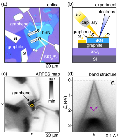
The measurements were carried out at the MAESTRO facility at the Advanced Light Source, Lawrence Berkeley National Laboratory. Using an achromatic focusing capillary, which simultaneously provides a high photon flux and a m beam-spot Ulstrup et al. (2019), we are able to collect high quality microARPES spectra that allow for a detailed analysis of many-body effects in graphene. The photon energy was set at 90 eV unless otherwise noted, and the optimum achieved energy- and -resolution were 40 meV and 0.01 Å-1, respectively. The measurements were carried out at room temperature. Our experimental configuration, which is sketched in Fig. 1(b), fully realizes in operando microARPES.
Our device is initially mapped by scanning the photon beam from the capillary over the same area as seen in the optical micrograph in Fig. 1(a). The resulting -dependent photoemission intensity is presented in Fig. 1(c). A corresponding snapshot of the -dispersion from the region marked by a circle in the map is shown in Fig. 1(d). One immediately notices a sharp Dirac cone due to the graphene flake in this region, as well as the onset of an intense band at a binding energy of 2.5 eV. The latter is consistent with the dispersion around the hBN valence band maximum Koch et al. (2018). The map in Fig. 1(c) has been composed from the - and -integrated intensity in the region enclosed by the dashed lines in Fig. 1(d), making the graphene flake clearly distinguishable between source and drain electrodes due to the presence of the graphene Dirac cone. We refer to the supplemental material for further characterization of the features in the map SMA . The arrows in Fig. 1(d) point to faint Dirac cone replicas that are consistent with the mini Brillouin zone of the graphene/hBN superlattice defined by the twist angle of 2.0∘ Wang et al. (2016); Ulstrup et al. (2019); SMA .
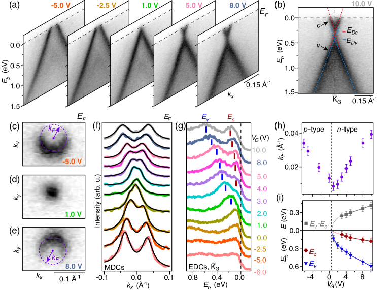
Detailed measurements of the -dispersion of the Dirac cone as a function of gate voltage () in our device are presented in Fig. 2. The series of snapshots around G in panels (a)-(b) and in the Supplementary Video demonstrate excellent control of both - and -type fillings of the Dirac cone, thereby giving access to the valence () and conduction () bands defined in panel (b). Each snapshot has been obtained from the full -dispersion around the Dirac cone, which simultaneously provides the circular Fermi surface, as shown for a subset of gate voltages in panels (c)-(e). Recently, similar in situ electrostatic doping experiments on graphene have displayed an energy gap at the Dirac crossing for -type doping Nguyen et al. (2019). Such a gap is likely to result from a slight misalignment of the detector scattering plane from the crystal axes, or stray fields affecting the electron trajectory, and is avoided in our measurements by careful alignment of the detector at each gate voltage step.
The radius that determines the size of the Fermi surface (see panels (c) and (e)) is found by extracting the -separation between the peak positions of the two linear branches at for each gate voltage. The peak positions are obtained using double Lorentzian fits of momentum distribution curves (MDCs) as shown in panel (f). The -dependence of the crossings between - and -branches is monitored through energy distribution curve (EDC) cuts at G as presented in panel (g). The crossing of the -branches is detected via a peak (see blue tick labeled ) that is fully below in our spectra for V. We find that the crossing of the -branches (see red tick labeled ) is separated in binding energy from the -crossing and that its corresponding peak is fully below for V. The full -dependence of and of the separation () determined from the MDC and EDC analyses are shown in panels (h)-(i). The doping dependence of signals the presence of many-body interactions, which are contained in the photohole spectral function, , that ARPES measures Bostwick et al. (2007). Here, is the quasiparticle dispersion around the Dirac point with the -dependent slope Sarma and Hwang (2013), and is the imaginary part of the self-energy that is proportional to the quasiparticle scattering rate. It is related to the full-width at half maximum () of the MDC fits as .
The many-body effects are investigated as a function of carrier density () using Efetov and Kim (2010). Fitting to the expected linear dependence on demonstrated in Fig. 3(a) and given by Novoselov et al. (2004), where is the elemental charge, leads to estimates of the capacitance per area ( nF/cm2) and the shift of the charge neutrality point ( V). Combining this dependence with the resistance () of the device measured in situ as seen in Fig. 3(b) SMA provides the doping-dependent sheet conductivity shown in Fig. 3(c). This leads to the room temperature mobility cm2/Vs, which appears reasonable when comparing with other graphene/hBN devices Dean et al. (2010). We address the scattering processes at that affect towards the end of this letter.
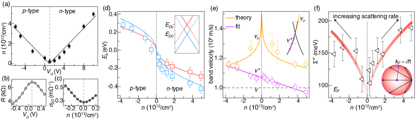
By combining the MDC fits at in Fig. 2(f) with a more detailed analysis over a binding energy range of 1 eV measured from the Fermi level SMA , we extract the doping-dependent many-body interactions in our device. This analysis shows that it is reasonable to assume a linear dependence of the () band below (above) the Dirac crossing. We therefore linearly extrapolate the fitted dispersion as demonstrated in Fig. 2(b) to obtain a more precise estimate of the binding energy of the Dirac crossings than the and values picked out in Fig. 2(g). The results are presented in Fig. 3(d) for the -crossing () for all dopings and the -crossing () for the four most strongly -type doped dispersions where the branches are sufficiently separated in to permit a reliable fit. The separation of the Dirac crossing is seen in Fig. 2(i) and Fig. 3(d) to vanish at charge neutrality, while it increases towards higher doping. This is a clear indication for electron-plasmon excitations Bostwick et al. (2010). We therefore use the one-particle Green’s function calculations describing these excitations in Ref. 29 to convert the separation into an estimate for the effective Coulomb coupling constant , where m/s is the bare band velocity, is the vacuum permittivity and is the background screening constant. We obtain for our graphene/hBN device. In completely unscreened suspended graphene one would find Elias et al. (2011); Sarma and Hwang (2013). The smaller value of in our sample is expected due to the underlying hBN, however the electron-electron interaction can still be rather substantial as observed in the spectral function of hydrogen intercalated graphene on silicon carbide where has a similar value as we find here on hBN Bostwick et al. (2010); Walter et al. (2011).
We investigate how the interaction strength in our device affects the doping-dependent shape of the Dirac cone by extracting the Fermi velocity () and the band velocity below the Dirac crossing. The values of for the dopings where we could perform a reliable fit are presented in Fig. 3(e) together with the analytic result for the renormalized Fermi velocity Sarma and Hwang (2013), where Å is the graphene lattice parameter. The theoretical result is shown via the orange curve for and exhibits a trend that is consistent with our data. Note that would be constant and equal to as shown by a horizontal dashed line in Fig. 3(e) in the fully screened limit given by . This is clearly not the case here where we instead find a sharpening effect of the cone towards charge neutrality, alluding to the situation in suspended graphene Elias et al. (2011). A substantially different behavior is found for the band velocity determined over an -range centered 300 meV below for all dopings in order to avoid confusing changes of the slope with the bare band dispersion Park et al. (2008). We find a continuous decrease of as the Dirac cone shifts to higher binding energies with increasing -type doping, as shown in Fig. 3(e), which is caused by the growing number of electron-hole pair scattering processes towards higher binding energies Bostwick et al. (2007); Sarma et al. (2007); Siegel et al. (2011). Our analysis affirms that the quasiparticle velocity in gated graphene on hBN is significantly doping-dependent due to the Coulomb interaction Sarma et al. (2007).
In Fig. 3(f) we examine the doping dependence of at determined from the MDC linewidths in Fig. 2(f). The behavior of is characterized by a suppression around charge neutrality and a near-symmetric increase with both - and -type doping, which appears to follow a -dependence with a constant offset of 70 meV. From this we can exclude doping-dependent long-range charge impurity scattering, because this leads to a -dependence of as found in alkali metal doped graphene on hBN Siegel et al. (2013). The constant offset and -dependence are consistent with short-range electron-defect scattering and electron-phonon interactions Calandra and Mauri (2007), which scale with the radius of the Fermi surface Efetov and Kim (2010), as illustrated in the insert in Fig. 3(f). These scattering processes at are ultimately responsible for the reduced mobility of our device.
We have simultaneously measured the transport properties and the doping dependence of the quasiparticle spectral function in graphene on hBN by noninvasively changing the carrier concentration with an electric field, providing access to many-body interactions for a wide range of energies and momenta. Combining the measurement of a global property such as electron mobility with -, - and spatially-resolved electronic excitations is a powerful approach that will be transformative for correlating fundamental interactions with different types of electronic behaviors observed in transport studies of quantum materials, including complex properties such as charge ordering and high temperature superconductivity. The intrinsic doping dependence of the spectral function holds the key to fully understanding the physics of these phenomena.
Acknowledgements.
J.K. is supported by the U.S. Department office of Science, Office of Basic Sciences, of the U.S. Department of Energy under Award Number DE-SC0020323. S. U. acknowledges financial support from VILLUM FONDEN under the Young Investigator Program (Grant No. 15375). The authors also acknowledge the Villum Centre of Excellence for Dirac Materials (Grant No. 11744). The Advanced Light Source is supported by the Director, Office of Science, Office of Basic Energy Sciences, of the U.S. Department of Energy under Contract No. DE-AC02-05CH11231. K.W. and T.T. acknowledge support from the EMEXT Element Strategy Initiative to Form Core Research Center, Grant Number JPMXP0112101001 and the CREST(JPMJCR15F3), JST.References
- Novoselov et al. (2004) K. S. Novoselov, A. K. Geim, S. V. Morozov, D. Jiang, Y. Zhang, S. V. Dubonos, I. V. Grigorieva, and A. A. Firsov, Science 306, 666 (2004).
- Zhang et al. (2005) Y. B. Zhang, Y. W. Tan, H. L. Stormer, and P. Kim, Nature 438, 201 (2005).
- Novoselov et al. (2005) K. S. Novoselov, A. K. Geim, S. V. Morozov, D. Jiang, M. I. Katsnelson, I. V. Grigorieva, S. V. Dubonos, and A. A. Firsov, Nature 438, 197 (2005).
- Sarma et al. (2007) S. D. Sarma, E. Hwang, and W. Tse, Physical Review B 75, 121406(R) (2007).
- Elias et al. (2011) D. C. Elias, R. V. Gorbachev, A. S. Mayorov, S. V. Morozov, A. A. Zhukov, P. Blake, L. A. Ponomarenko, I. V. Grigorieva, K. S. Novoselov, F. Guinea, and A. K. Geim, Nature Physics 7, 701 (2011).
- Du et al. (2009) X. Du, I. Skachko, F. Duerr, A. Luican, and E. Y. Andrei, Nature 462, 192 (2009).
- Bolotin et al. (2009) K. I. Bolotin, F. Ghahari, M. D. Shulman, H. L. Stormer, and P. Kim, Nature 462, 196 (2009).
- Mayorov et al. (2012) A. S. Mayorov, D. C. Elias, I. S. Mukhin, S. V. Morozov, L. A. Ponomarenko, K. S. Novoselov, A. K. Geim, and R. V. Gorbachev, Nano Letters 12, 4629 (2012).
- Efetov and Kim (2010) D. K. Efetov and P. Kim, Physical Review Letters 105, 256805 (2010).
- Zhang et al. (2008) Y. Zhang, V. W. Brar, F. Wang, C. Girit, Y. Yayon, M. Panlasigui, A. Zettl, and M. F. Crommie, Nature Physics 4, 627 (2008).
- Bostwick et al. (2007) A. Bostwick, T. Ohta, T. Seyller, K. Horn, and E. Rotenberg, Nature Physics 3, 36 (2007).
- Hwang and Sarma (2008) E. Hwang and S. D. Sarma, Physical Review B 77, 081412(R) (2008).
- Basov et al. (2014) D. N. Basov, M. M. Fogler, A. Lanzara, F. Wang, and Y. Zhang, Rev. Mod. Phys. 86, 959 (2014).
- Bostwick et al. (2010) A. Bostwick, F. Speck, T. Seyller, K. Horn, M. Polini, R. Asgari, A. H. MacDonald, and E. Rotenberg, Science 328, 999 (2010).
- Chen et al. (2008) J. H. Chen, C. Jang, S. Adam, M. S. Fuhrer, E. D. Williams, and M. Ishigami, Nature Physics 4, 377 (2008).
- Siegel et al. (2013) D. A. Siegel, W. Regan, A. V. Fedorov, A. Zettl, and A. Lanzara, Physical Review Letters 110, 146802 (2013).
- Ulstrup et al. (2014) S. Ulstrup, M. Andersen, M. Bianchi, L. Barreto, B. Hammer, L. Hornekær, and P. Hofmann, 2D Materials 1, 025002 (2014).
- Siegel et al. (2011) D. A. Siegel, C.-H. Park, C. Hwang, J. Deslippe, A. V. Fedorov, S. G. Louie, and A. Lanzara, Proceedings of the National Academy of Sciences 108, 11365 (2011).
- Ulstrup et al. (2016) S. Ulstrup, M. Schüler, M. Bianchi, F. Fromm, C. Raidel, T. Seyller, T. Wehling, and P. Hofmann, Phys. Rev. B 94, 081403 (2016).
- Katoch et al. (2018) J. Katoch, S. Ulstrup, R. J. Koch, S. Moser, K. M. McCreary, S. Singh, J. Xu, B. T. Jonker, R. K. Kawakami, A. Bostwick, E. Rotenberg, and C. Jozwiak, Nature Physics 14, 355 (2018).
- Joucken et al. (2019) F. Joucken, J. Avila, Z. Ge, E. A. Quezada-Lopez, H. Yi, R. Le Goff, E. Baudin, J. L. Davenport, K. Watanabe, T. Taniguchi, M. C. Asensio, and J. Velasco, Nano Letters 19, 2682 (2019).
- Nguyen et al. (2019) P. V. Nguyen, N. C. Teutsch, N. P. Wilson, J. Kahn, X. Xia, A. J. Graham, V. Kandyba, A. Giampietri, A. Barinov, G. C. Constantinescu, N. Yeung, N. D. M. Hine, X. Xu, D. H. Cobden, and N. R. Wilson, Nature 572, 220 (2019).
- Ulstrup et al. (2019) S. Ulstrup, R. J. Koch, S. Singh, K. M. McCreary, B. T. Jonker, J. T. Robinson, C. Jozwiak, E. Rotenberg, A. Bostwick, J. Katoch, and J. A. Miwa, “Direct observation of minibands in twisted heterobilayers,” (2019), Science Advances, in press, arXiv:1904.06681 .
- (24) “See Supplemental Material for details of device fabrication and microARPES sample mounting, for spatial dependence of device photoemission intensity, for core level data, for relative orientations of Brillouin zones, for details on quasiparticle spectral function analysis and for resistance measurements during beam exposure.” .
- Koch et al. (2018) R. J. Koch, J. Katoch, S. Moser, D. Schwarz, R. K. Kawakami, A. Bostwick, E. Rotenberg, C. Jozwiak, and S. Ulstrup, Phys. Rev. Materials 2, 074006 (2018).
- Wang et al. (2016) E. Wang, X. Lu, S. Ding, W. Yao, M. Yan, G. Wan, K. Deng, S. Wang, G. Chen, L. Ma, J. Jung, A. Fedorov, Y. Zhang, G. Zhang, and S. Zhou, Nature Physics 12, 1111 (2016).
- Sarma and Hwang (2013) S. D. Sarma and E. Hwang, Physical Review B 87, 045425 (2013).
- Dean et al. (2010) C. Dean, A. Young, I. Meric, C. Lee, L. Wang, S. Sorgenfrei, K. Watanabe, T. Taniguchi, P. Kim, K. Shepard, and J. Hone, Nature Nanotechnology 5, 722 (2010).
- Walter et al. (2011) A. L. Walter, A. Bostwick, K.-J. Jeon, F. Speck, M. Ostler, T. Seyller, L. Moreschini, Y. J. Chang, M. Polini, R. Asgari, A. H. MacDonald, K. Horn, and E. Rotenberg, Physical Review B 84, 085410 (2011).
- Park et al. (2008) C. Park, F. Giustino, J. McChesney, A. Bostwick, T. Ohta, E. Rotenberg, M. Cohen, and S. Louie, Physical Review B 77, 113410 (2008).
- Calandra and Mauri (2007) M. Calandra and F. Mauri, Phys. Rev. B 76, 205411 (2007).