Phys. Rev. Applied 13 (2020)
2020 Collection on 2D Materials and Devices
Periodically Gated Bilayer Graphene as an Electronic Metamaterial
Abstract
We study ballistic transport in periodically gated bilayer graphene as a candidate for a 2D electronic metamaterial. Our calculations use the equilibrium Green function formalism and take into account quantum corrections to charge density changes induced by a periodically modulated top gate voltage. Our results reveal an intriguing interference-like pattern, similar to that of a Fabry-Pérot interferometer, in the resistance map as a function of the voltage applied to the extended bottom gate and applied to the periodic top gate.
I Introduction
Photonic metamaterials are artificial structures used to control propagation of light waves Veselago (1968). Their frequency-dependent electromagnetic response in terms of transmission, reflection and refraction can be tailored using designer periodic arrays of structural elements spaced closer than the wavelength of light Kosaka et al. (1998); Smith et al. (2000); Shelby et al. (2001); Pendry et al. (2006); Stockman (2004); Yao et al. (2008); Mikhailov and Ziegler (2007); Valentine et al. (2008, 2009); Ni et al. (2015); Xiang et al. (2014); Lv et al. (2016); Shi et al. (2018). Same as a photonic metamaterial is capable of manipulating a coherent electromagnetic wave Veselago (1968), so should an electronic metamaterial be able to manipulate a coherent wave of electrons Dragoman and Dragoman (1999, 2007). Same as propagation of light can be controlled by periodically modulating the index of refraction and speed of light in a three-dimensional (3D) crystal Yao et al. (2008); Valentine et al. (2008), so can the propagation of electrons be controlled by modulating the electrostatic potential and Fermi velocity in a two-dimensional (2D) graphene bilayer Young and Kim (2011); Varlet et al. (2014); Du et al. (2018); Kraft et al. (2018). Same qualitative behavior should be expected of coherent waves of electrons and photons with the main difference that the electrostatic potential is much easier to modulate than the index of refraction Young and Kim (2011). Then, phenomena including scattering, interference, diffraction of light and uncommon behavior of photons in an optical metamaterial Kosaka et al. (1998); Smith et al. (2000); Shelby et al. (2001); Pendry et al. (2006); Yao et al. (2008); Valentine et al. (2008, 2009); Ni et al. (2015) should occur on a wider and more flexible range when manipulating electrons in an electronic metamaterial. In particular, a periodically gated 2D semiconductor may display the same transmission behavior for electrons Tsu and Esaki (1973) as a distributed Bragg reflector (DBR) does for photons Reinhart et al. (1975); Tsang and Wang (1976).
To explore the possibility of constructing a 2D electronic metamaterial, we study theoretically the propagation of electrons in periodically gated bilayer graphene. Our calculations use the equilibrium Green function formalism to describe ballistic transport in bilayer graphene (BLG) and consider quantum corrections to charge density changes induced by a periodic modulation of the top gate voltage. Our results reveal an intriguing interference-like pattern, similar to that of a Fabry-Pérot interferometer, in the resistance map as a function of the voltage applied to the extended bottom gate and applied to the periodic top gate.
Due to its atomic-scale perfection and unique electronic structure, monolayer graphene (MLG) has emerged as an ideal 2D material to study charge transport Novoselov et al. (2004). Much attention has been paid to ballistic transport of electrons and suppression of backscattering by Klein tunneling in MLG, including the effect of junctions, local and periodic gating, interaction with the substrate and presence of magnetic field Katsnelson et al. (2006); Shytov et al. (2008); Beenakker (2008); Young and Kim (2009); Ramezani Masir et al. (2010); Dubey et al. (2013); Liu (2013); Yankowitz et al. (2012); Ponomarenko et al. (2013); Chen et al. (2016); Drienovsky et al. (2014, 2017, 2018). The band structure of MLG at the six Fermi points in the Brillouin zone is characterized by Dirac cones, formally describing massless particles with constant independent of doping.
Our study is devoted to periodically gated BLG which, same as MLG, is a semimetal. Unlike in MLG, scattering is not suppressed by Klein tunneling due to the lowered symmetry of BLG. In absence of Klein tunneling, the resistance of BLG can be tuned to be very high. The band structure of BLG is qualitatively different from MLG, as it is characterized by parabolas and not Dirac cones near . Consequently, and thus the wavelength of electrons can be modulated by local doping caused by changing the electrostatic potential. Thus, the BLG system appears to be a better candidate for electron optics than MLG, which we will also discuss for the sake of reference. The possibility of constructing the electronic counterpart of an optical DBR has not been explored so far.
II Structure and Functionality of Periodically Gated BLG
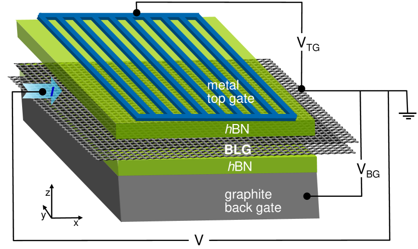
The schematic of a recently fabricated device Xia , consisting of periodically gated BLG sandwiched in-between inert BN layers, is presented in Fig. 1. The BLG channel is contacted by metal leads at the source and the drain ends and is separated by an nm thick BN layer from the bottom electrode and by an nm thick BN layer from the top electrode. The top electrode consists of a periodic array of parallel, nm wide wires, separated by nm. The bottom gate voltage regulates the doping level of the channel, whereas the top gate voltage modulates the electrostatic potential along the channel. The device performance is characterized by the resistance between source and drain.
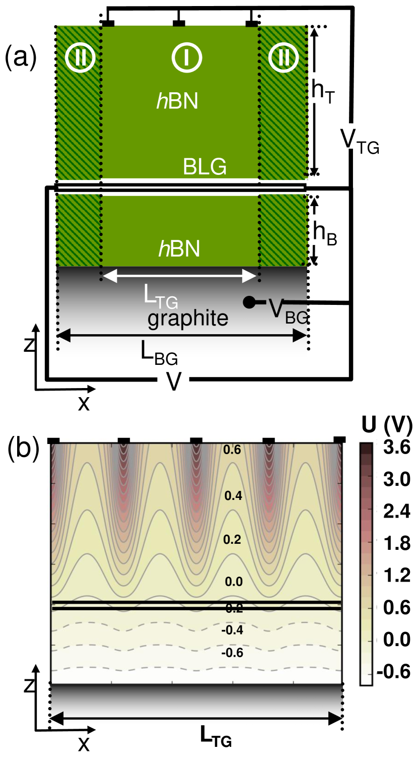
To provide an adequate description of the gated BLG device under operating conditions, we distinguish its components and their function in the schematic cross-section provided in Fig. 2(a). Only the central region of the device, labeled (I), lies between the non-uniform top gate (TG) of length , formed of a metal wire array, and the bottom gate (BG) of length , formed of a graphite slab. This is the region of interest for electron optics to be discussed below.
Even though region (II), which lies in-between region (I) and the contacts, may be of lesser interest, it still needs to be addressed in the transport study. This region is above the BG and thus affected by , but outside the range of the TG and thus unaffected by . Key to the interpretation of the resistance in region (II) is the interface between BLG and BN layers above and below the channel. There is only negligible electronic interaction between graphene layers and the surrounding BN due to its eV wide band gap Watanabe et al. (2004). Even if the BLG were perfectly aligned with BN, the 1.8% lattice mismatch would give rise to a Moiré superlattice Yankowitz et al. (2012); Ponomarenko et al. (2013). Minor lattice relaxation in the graphene layer caused by their interaction with BN would then modulate periodically the potential in the graphitic channel, giving rise to second-generation Dirac points Yankowitz et al. (2012); Ponomarenko et al. (2013); Dean et al. (2013); Jung et al. (2015); Wallbank et al. (2015). In perfectly aligned BLG/BN superlattices, we expect the electronic density of states (DOS) to vanish at as a consequence of first-generation Dirac points at the charge neutrality level and at eV below and above as a consequence of newly formed second-generation Dirac points. For , is located at first-generation Dirac points, resulting in high resistance that is independent of and represented by a line in the resistance map. Applying a bottom gate voltage induces a nonzero charge density in the channel, where is the dielectric constant and is the thickness of the lower BN layer, as defined in Fig. 2(a). We find that the charge density needed to reach the secondary Dirac points may be induced by V when using Geick et al. (1966) and nm in the BLG device. The large resistance at this value of is again independent of , giving rise to a second parallel line in the resistance. For voltages other than V and V, the resistance map reflects only the behavior in region (I).
III Results
III.1 Transport in Periodically Gated BLG at
To determine the resistance pattern associated with the central region (I) of interest, we first calculate the electronic structure of BLG and the electrostatic potential within the plane of the channel as a function of and . For a given combination, the propagation of ballistic electrons and the net resistance of the gated BLG device is evaluated using the equilibrium Green function formalism.
As indicated in Figs. 1 and 2(a), we denote the transport direction and the direction of the TG wires by . The width and length of the periodically gated region is much larger than any other dimensions in the device and may be considered infinite. Due to this large size, atomistic calculation of the entire structure is out of the question and would only complicate the interpretation of transport results in periodically gated BLG. In the cryogenic regime with a very small applied source-bias voltage, transport in the BLG channel can be considered to be ballistic and attributed to propagation of low-energy charge carriers in a periodically modulated potential .
The low-energy Hamiltonian of a free-standing, ungated BLG can be written as McCann and Koshino (2013)
| (1) |
Here we use with to describe the carrier momentum with respect to the Fermi momentum at the Fermi point in the corner of the hexagonal Brillouin zone. The tight-binding parameters describing these systems are Tomanek and Louie (1988) the intra-layer nearest neighbor hopping integral eV and the inter-layer nearest neighbor hopping integral eV. This yields , where Å is the intra-layer nearest neighbor distance. Only the diagonal matrix elements will be affected by the modulation of the potential in the field of the periodic top gate, since the top gate period is much larger than the interatomic spacing.
The two low-energy bands of are
| (2) |
where is close to the Fermi momentum . describes the dispersion in the conduction band and that in the valence band.
In BLG gated by a periodic top and a uniform bottom gate, the net electron number density varies periodically along the transport direction and is constant in the direction. In BLG with isotropic band dispersion at , we find
| (3) |
where is the Fermi wavevector at position . There is particle-hole symmetry with positive for electron and negative for hole doping.
The dependence of the charge density and the Fermi momentum on is in response to the periodic electrostatic potential in the plane of the BLG. With the contact lead at the drain end at ground potential, which sets within the BLG, this potential is given by
| (4) |
where is the absolute value of the electron charge. The subscript in the expression for in Eq. (2) is either in case of electron doping or in case of hole doping. The sign of is the same as that of and .
In principle, could be obtained for any gate geometry by solving the Poisson equation Liu (2013). To avoid this calculation for every combination of and , we use an alternate approach. We note that in BLG exposed to the periodic electrostatic potential caused by the TG voltage and the BG voltage , can be expressed by
| (5) |
Here, the doping charge density has been related to changes in the potential by the position-dependent partial capacitances Liu (2013) of the top gate and of the bottom gate. The above expression can be rewritten as
| (6) | |||||
which defines a new quantity, namely the classical net electron number density . This quantity depends on the position within the BLG, considered to be a classical metal, the gate geometry and the gate voltages and . is nominally defined by and can be calculated in the BLG plane using classical electrostatics for the specific gate geometry. For a given charge density distributed uniformly across the top gate wires, which are separated by a dielectric of thickness and dielectric constant from the grounded BLG, we can numerically determine and the electric field in the entire region using the image-charge technique, which also guarantees a constant zero potential in the BLG layer. Integrating the electric field between the TG and the BLG yields the corresponding value of , and the same approach can be used for the bottom gate. We note that is proportional to and is proportional to , providing quantitative values for and . is a nominal voltage value taken to be V.
We note that considering the grounded BLG channel as a classical metal, nonzero and can induce periodic variation in the classical density while keeping the electrostatic potential constant within the BLG. The fact that BLG is not a classical metal, but a semi-metal with a vanishing DOS at , necessitates further consideration. Unlike in a classical metal with a large DOS at , periodic variations of in BLG with a small DOS at will cause a nominal periodic modulation of . To keep constant, the classical carrier density within the BLG will be modified by what we call a quantum correction . In this better description, the periodic electrostatic potential in the semimetallic BLG is no longer constant and will play an important role. Then, also for a given between the BG and the BLG will no longer be constant. In the region between the TG and BLG, quantum corrections dampen the oscillations in at constant . The electrostatic potential associated with the quantum corrected carrier density within the BLG, caused by V and V, is shown in Fig. 2(b) for the central region (I) and between the TG and the bottom gate.
Being able to determine the electrostatic potential and the position-dependent Fermi momentum using Eq. (7), we can express the position-dependent potential energy of low-energy electrons or holes in BLG by
| (8) |
For BLG in the periodic potential energy surface , the system becomes a superlattice with the lattice constant along the direction, with nm for the device shown in Fig. 1. The low-energy bands of this superlattice are given by the eigenvalues of
| (9) |
Here, the wavevector with respect to the Fermi momentum, defined in Eq. (1), has become the operator due to the dependence of the diagonal elements. Since varies very slowly and thus can be represented by only a small number of Fourier components, can be diagonalized using as basis the eigenfunctions of the free-standing with the momentum vectors in the superlattice geometry.
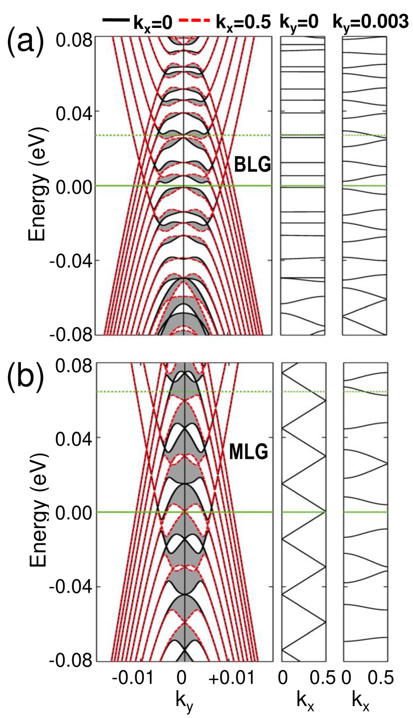
The electronic band structure of the gated BLG is presented in Fig. 3(a) for representative values V and V. The data presented in the left panel display at two values of in the short Brillouin zone of the superlattice. The shaded regions in-between the bands indicate the range of band dispersion and white regions indicate local band gaps. We note that BLG becomes charge neutral when all bands below the charge-neutrality level, shown by the green dashed line, become occupied. The band dispersion along , shown for two values in the two right panels, indicates that bands are almost flat and separated by gaps near the zero-energy level. We find that at other values of and the band structure is qualitatively very similar, but shifts periodically with respect to .
Conductance is known to be quantized in a system with a finite cross-section in the ballistic regime Datta (1995). To interpret transport in the device we investigate, we need to consider its finite width m. Allowed eigenstates will then be standing waves normal to the transport direction and will be quantized. For each value, every band that crosses the zero-energy level along of the superlattice provides one conduction channel. Each conduction channel contributes a conductance quantum . Then, the total conductance is obtained by counting the number of values associated with bands dispersing along the direction that cross the zero-energy level. The total number of conduction channels in the real device of width becomes
| (10) |
where allowed values are integer multiples of and is the average transmission probability per mode. At K, an allowed state with given is either occupied or empty. In that case, it will fully contribute to transmission with probability if a band crosses the zero-energy level along for a given value, or otherwise not contribute at all, so that .
Transport calculations for a ballistic device at a non-zero source-drain voltage are typically performed using the non-equilibrium Green function formalism Damle et al. (2003). In the device we consider, which is driven by a source of very small constant current, is negligibly small. In that case, transport can be calculated using the equilibrium Green function that describes the electronic structure of the unperturbed system.
The resistance of the central region (I) is then given by . To obtain a smooth map of at K as a function of and , we have convoluted the conductance with a Gaussian function at each and obtained
| (11) |
where is the full width at half maximum of the Gaussian function. The smooth resistance map is then obtained and compared with the experimental results.
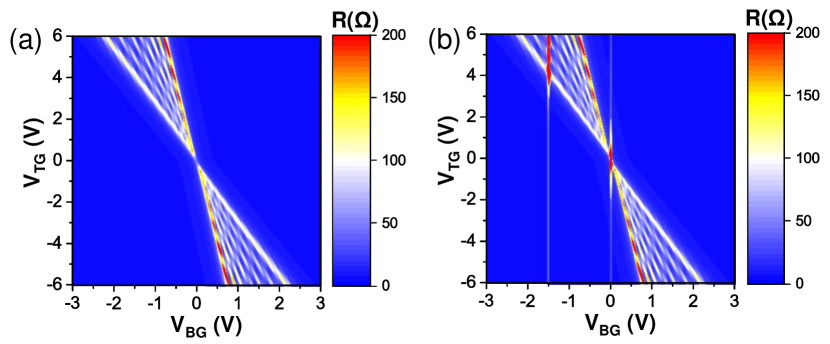
Figure 4(a) shows the calculated smooth resistance map of the central region (I) and Fig. 4(b) that of the entire device with nm and nm.
Electrons are doped into BLG at positive gate voltages and holes at negative gate voltages. At negative bottom gate voltages and negative or small positive top gate voltages , BLG is hole doped everywhere and thus shows low resistance, represented by the uniform dark blue color of the bottom left region of the resistance map in Fig. 4(a). At large positive values of and , on the other hand, BLG is electron doped everywhere and thus also shows low resistance, as indicated by the same dark blue color of the top right region in the resistance map. At given combined with moderate values, and alternately at given combined with moderate values, regions of hole and electron doping in BLG alternate along the transport direction . In that case, also the sign of and alternates along the -direction and electrons, which have been injected at the zero-energy level at the source contact, have to tunnel through a periodic array of potential barriers. Then, constructive or destructive interference may cause significant oscillations in the net resistance as seen in Fig. 4(a), similar to a Fabry-Pérot interferometer.
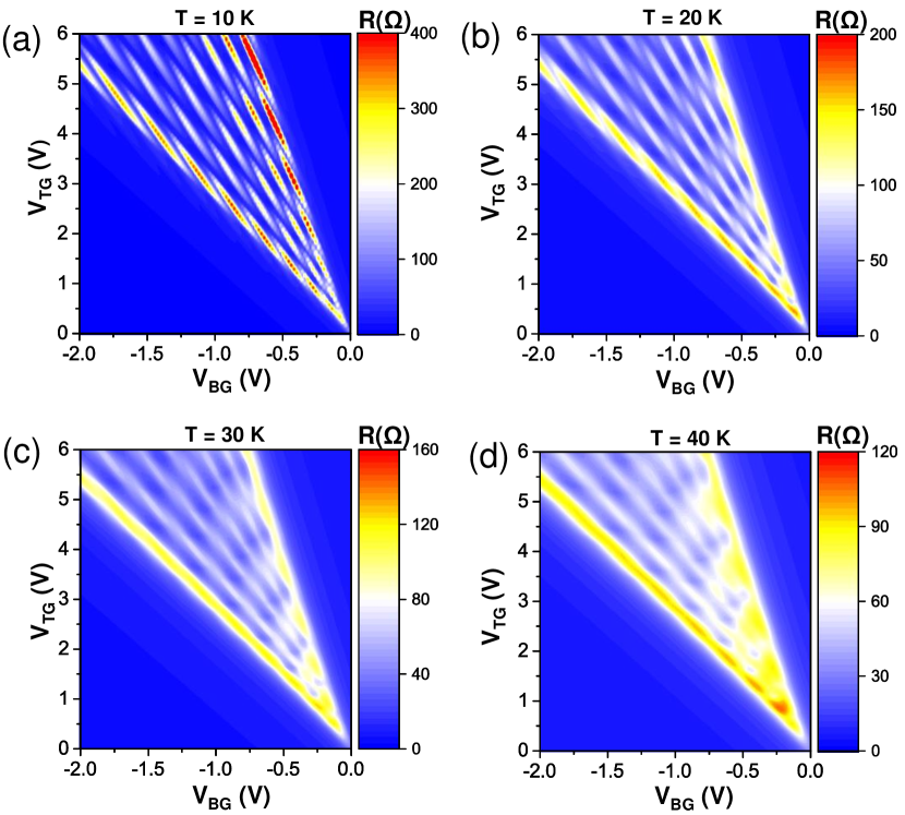
In order to understand the origin of oscillations of in the resistance map, we refer to the calculated band structure of the BLG superlattice in a constant potential, shown in Fig. 3(a). Results shown in the middle panel of Fig. 3(a) indicate that the band dispersion along near of the superlattice is very small. The white regions in the left panel of Fig. 3(a) correspond to band gaps near , which are not affected by this small band dispersion along . When the zero-energy level lies in such a local gap, electrons injected at can not propagate, corresponding to a high resistance. At somewhat larger values such as , the band dispersion along increases, as seen in the right panel of Fig. 3(a). In that case, a momentum may be found, at which a band crosses , thus forming a conductance channel and reducing the resistance. As seen in the left panel of Fig. 3(a), the band dispersion along decreases again at still larger values of , thus lowering the likelihood of transmission and increasing the resistance. As mentioned earlier, this discussion considered charge transport in the special case of a constant potential. Changing the gate voltages changes and modulates the potential along the transport direction. Gradual changes in the potential move locally the band structure up or down in energy with respect to , thus changing the number of bands crossing along . A transmission channel will only then contribute a conductance quantum if it is open for all values of . The above reasoning explains the appearance of alternating conductance and resistance maxima associated with changing gate voltages.
III.2 Effect of Temperature on Transport in Periodically Gated BLG
Unlike at K discussed so far, allowed states near may be partially occupied by the Fermi-Dirac distribution at . Then, the average transmission probability per mode, introduced in Eq. (10), may take a value in the entire range for each band along . Accommodating the band dispersion along , we find Datta (1995)
| (12) |
where we have given all energies with respect to . We have further noted a near-linear dispersion of the -th band along , ranging from to , for a given value of . is the Boltzmann constant.
III.3 Effect of Geometry on Transport in Periodically Gated BLG
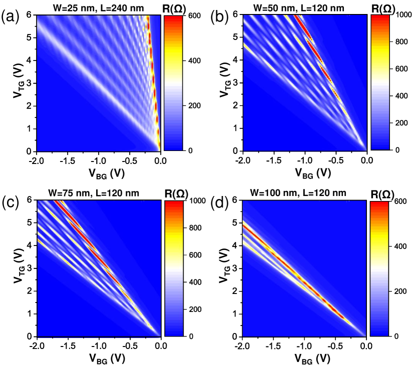
The resistance map also depends on the geometry of the BLG device. To inspect this dependence, we present in Fig. 6 the calculated resistance map of BLG devices with different values of the width of each wire and the inter-wire distance within the periodic top gate. As seen in Fig. 6(a), high-resistance lines become continuous in case that . Results in Fig. 6(b)-6(d) indicate that for a fixed , the series of high-resistance lines tilts and their number decreases with increasing .
III.4 Comparison with Periodically Gated MLG
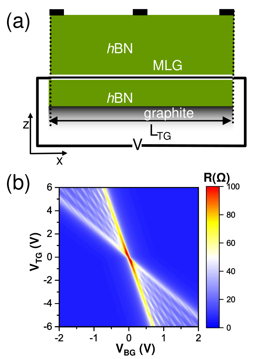
As a matter of reference, we compare in the following our results for BLG to MLG in the same device geometry, depicted in Fig. 7(a). In consideration of the absence of Klein tunnelling in BLG due to the interlayer coupling, we have used BLG rather than monolayer graphene (MLG) here as the channel to demonstrate such a resistance map, as analyzed below. The only difference between the MLG and BLG device is the simpler Hamiltonian, which is given in analogy to Eq. (1) by
| (13) |
and which leads to the band structure presented in Fig. 3(b).
The MLG-based device we consider is nearly identical to that shown in Figs. 1 and 2(a), but with BLG replaced by MLG as the channel. The calculated resistance map of the MLG-based device, shown in Fig. 7(b), displays a similar pattern as the BLG device. A notable difference between the two is a much lower contrast in the MLG than in the BLG device, with the resistance peak values for MLG being much lower. In addition, compared with MLG, the resistance peaks for BLG are wider and higher, and the resistance valleys are also wider and shallower. We also note that in the resistance map without convolution, the MLG device has many more resistance peaks. These peaks in are well separated, but their values are much lower values than the BLG device.
These features in the resistance map of MLG are reflected in its band structure, shown in Fig. 3(b). As seen in the left panel of Fig. 3(b), bands with and with always cross at in MLG. Even though there is no gap opening, placing the zero-energy level at this band crossing at gives rise to a resistance maximum. In BLG, on the other hand, the interlayer coupling opens local gaps around , resulting in a much higher resistance of the BLG in comparison to the MLG device.
As seen in the middle panel of Fig. 3(b), the MLG bands at are highly dispersive and the energy spectrum is free of gaps. Also, the states at both and are doubly degenerate. Thus, states contribute one conduction mode for all values of and . Absence of scattering in this periodically gated channel is another demonstration of Klein tunneling in MLG.
We note that the double-degeneracy of these eigenstates of free-standing MLG is protected in the 1D periodic potential by the symmetry operation
| (14) |
where is the complex conjugation operator. This can be explained simply, since the Hamiltonian for MLG
| (15) |
remains invariant under , so that the degeneracy of the above-mentioned eigenstates is not broken by any periodic potential . We should also note that this symmetry protection only occurs for electrons with corresponding to normal incidence on the wires. There is no symmetry protection for off-normal incidence, so that such electrons may be reflected, giving rise to an interference pattern in the resistance map. Nevertheless, since is near-zero for most electrons contributing to transport in the device, most carriers are transmitted and do not contribute to the interference pattern in the resistance map. Since only a minority of electrons undergo reflection and interference in MLG, corresponding resistance maxima are less pronounced in the resistance map of MLG.
The situation is different in BLG, where the interlayer hopping integral breaks the symmetry. As seen in the middle panel of Fig. 3(a), BLG bands at show very little dispersion along near due to the interlayer interaction. Since these bands do not cross , the corresponding states do not contribute to conduction, thus lowering the off-current and increasing the contrast in the resistance map.
As mentioned earlier, BLG is doped by electrons at positive gate voltages and by holes at negative voltages. Even though the magnitude of the Fermi velocity does not depend on the sign of the doping carriers, the direction of in electron-doped BLG is opposite to that of hole-doped BLG. In some respect, this is parallel to the particle-hole symmetry found in BLG and MLG.
IV Summary and Conclusions
In conclusion, we have studied the propagation of electrons in periodically gated bilayer graphene as a way to construct a 2D electronic metamaterial. We identified an intriguing interference-like pattern, similar to that of a Fabry-Pérot interferometer, in the resistance map in response to doping and potential modulation provided by the extended bottom gate and the periodic top gate. We provided a quantitative explanation for the observations by considering quantum corrections to the position-dependent potential in the channel region and the equilibrium Green function formalism that describes ballistic transport in BLG. We find periodically gated BLG to be a suitable candidate for a distributed Bragg reflector for electrons.
Acknowledgements.
This study has been inspired by Siqi Wang, Mervin Zhao, Changjian Zhang, Sui Yang, Yuan Wang, Kenji Watanabe, Takashi Taniguchi, James Hone, and Xiang Zhang, who kindly discussed their experimental results with us. X.L. and D.T. thank Dan Liu for fruitful discussions. X.L. acknowledges support by the China Scholarship Council and the National Natural Science Foundation of China (Grant No. 11974312). D.T. acknowledges financial support by the NSF/AFOSR EFRI 2-DARE grant number EFMA-1433459. Computational resources have been provided by the Michigan State University High Performance Computing Center.References
- Veselago (1968) V. G. Veselago, “The electrodynamics of substances with simultaneously negative values of and ,” Phys. Usp. 10, 509–514 (1968).
- Kosaka et al. (1998) Hideo Kosaka, Takayuki Kawashima, Akihisa Tomita, Masaya Notomi, Toshiaki Tamamura, Takashi Sato, and Shojiro Kawakami, “Superprism phenomena in photonic crystals,” Phys. Rev. B 58, R10096–R10099 (1998).
- Smith et al. (2000) D. R. Smith, Willie J. Padilla, D. C. Vier, S. C. Nemat-Nasser, and S. Schultz, “Composite medium with simultaneously negative permeability and permittivity,” Phys. Rev. Lett. 84, 4184–4187 (2000).
- Shelby et al. (2001) R. A. Shelby, D. R. Smith, and S. Schultz, “Experimental verification of a negative index of refraction,” Science 292, 77–79 (2001).
- Pendry et al. (2006) J. B. Pendry, D. Schurig, and D. R. Smith, “Controlling electromagnetic fields,” Science 312, 1780–1782 (2006).
- Stockman (2004) Mark I. Stockman, “Nanofocusing of optical energy in tapered plasmonic waveguides,” Phys. Rev. Lett. 93, 137404 (2004).
- Yao et al. (2008) Jie Yao, Zhaowei Liu, Yongmin Liu, Yuan Wang, Cheng Sun, Guy Bartal, Angelica M. Stacy, and Xiang Zhang, “Optical negative refraction in bulk metamaterials of nanowires,” Science 321, 930–930 (2008).
- Mikhailov and Ziegler (2007) S. A. Mikhailov and K. Ziegler, “New electromagnetic mode in graphene,” Phys. Rev. Lett. 99, 016803 (2007).
- Valentine et al. (2008) Jason Valentine, Shuang Zhang, Thomas Zentgraf, Erick Ulin-Avila, Dentcho A Genov, Guy Bartal, and Xiang Zhang, “Three-dimensional optical metamaterial with a negative refractive index,” Nature 455, 376 (2008).
- Valentine et al. (2009) Jason Valentine, Jensen Li, Thomas Zentgraf, Guy Bartal, and Xiang Zhang, “An optical cloak made of dielectrics,” Nature Mater. 8, 568 (2009).
- Ni et al. (2015) Xingjie Ni, Zi Jing Wong, Michael Mrejen, Yuan Wang, and Xiang Zhang, “An ultrathin invisibility skin cloak for visible light,” Science 349, 1310–1314 (2015).
- Xiang et al. (2014) Yuanjiang Xiang, Xiaoyu Dai, Jun Guo, Han Zhang, Shuangchun Wen, and Dingyuan Tang, “Critical coupling with graphene-based hyperbolic metamaterials,” Sci. Rep. 4, 5483 (2014).
- Lv et al. (2016) T. T. Lv, Y. X. Li, H. F. Ma, Z. Zhu, Z. P. Li, C. Y. Guan, J. H. Shi, H. Zhang, and T. J. Cui, “Hybrid metamaterial switching for manipulating chirality based on vo2 phase transition,” Sci. Rep. 6, 23186 (2016).
- Shi et al. (2018) Jinhui Shi, Zhongjun Li, David K. Sang, Yuanjiang Xiang, Jianqing Li, Shuang Zhang, and Han Zhang, “THz photonics in two dimensional materials and metamaterials: properties, devices and prospects,” J. Mater. Chem. C 6, 1291–1306 (2018).
- Dragoman and Dragoman (1999) D. Dragoman and M. Dragoman, “Optical analogue structures to mesoscopic devices,” Progress in Quantum Electronics 23, 131 – 188 (1999).
- Dragoman and Dragoman (2007) D. Dragoman and M. Dragoman, “Metamaterials for ballistic electrons,” J. Appl. Phys. 101, 104316 (2007).
- Young and Kim (2011) Andrea F Young and Philip Kim, “Electronic transport in graphene heterostructures,” Annu. Rev. Condens. Matter Phys. 2, 101–120 (2011).
- Varlet et al. (2014) Anastasia Varlet, Ming-Hao Liu, Viktor Krueckl, Dominik Bischoff, Pauline Simonet, Kenji Watanabe, Takashi Taniguchi, Klaus Richter, Klaus Ensslin, and Thomas Ihn, “Fabry-Pérot interference in gapped bilayer graphene with broken anti-Klein tunneling,” Phys. Rev. Lett. 113, 116601 (2014).
- Du et al. (2018) Renjun Du, Ming-Hao Liu, Jens Mohrmann, Fan Wu, Ralph Krupke, Hilbert von Löhneysen, Klaus Richter, and Romain Danneau, “Tuning anti-Klein to Klein tunneling in bilayer graphene,” Phys. Rev. Lett. 121, 127706 (2018).
- Kraft et al. (2018) Rainer Kraft, Jens Mohrmann, Renjun Du, Pranauv Balaji Selvasundaram, Muhammad Irfan, Umut Nefta Kanilmaz, Fan Wu, Detlef Beckmann, Hilbert von Löhneysen, Ralph Krupke, Anton Akhmerov, Igor Gornyi, and Romain Danneau, “Tailoring supercurrent confinement in graphene bilayer weak links,” Nature Communications 9, 1722 (2018).
- Tsu and Esaki (1973) R. Tsu and L. Esaki, “Tunneling in a finite superlattice,” Appl. Phys. Lett. 22, 562–564 (1973).
- Reinhart et al. (1975) F. K. Reinhart, R. A. Logan, and C. V. Shank, “GaAs-AlxGa1-xAs injection lasers with distributed Bragg reflectors,” Appl. Phys. Lett. 27, 45–48 (1975).
- Tsang and Wang (1976) Won-Tien Tsang and Shyh Wang, “GaAs-Ga1-xAlxAs double-heterostructure injection lasers with distributed Bragg reflectors,” Appl. Phys. Lett. 28, 596–598 (1976).
- Novoselov et al. (2004) K. S. Novoselov, A. K. Geim, S. V. Morozov, D. Jiang, Y. Zhang, S. V. Dubonos, I. V. Grigorieva, and A. A. Firsov, “Electric field effect in atomically thin carbon films,” Science 306, 666–669 (2004).
- Katsnelson et al. (2006) MI Katsnelson, KS Novoselov, and AK Geim, “Chiral tunnelling and the Klein paradox in graphene,” Nature Phys. 2, 620 (2006).
- Shytov et al. (2008) Andrei V. Shytov, Mark S. Rudner, and Leonid S. Levitov, “Klein backscattering and Fabry-Pérot interference in graphene heterojunctions,” Phys. Rev. Lett. 101, 156804 (2008).
- Beenakker (2008) C. W. J. Beenakker, “Colloquium: Andreev reflection and Klein tunneling in graphene,” Rev. Mod. Phys. 80, 1337–1354 (2008).
- Young and Kim (2009) Andrea F Young and Philip Kim, “Quantum interference and Klein tunnelling in graphene heterojunctions,” Nature Phys. 5, 222 (2009).
- Ramezani Masir et al. (2010) M. Ramezani Masir, P. Vasilopoulos, and F. M. Peeters, “Fabry-Pérot resonances in graphene microstructures: Influence of a magnetic field,” Phys. Rev. B 82, 115417 (2010).
- Dubey et al. (2013) Sudipta Dubey, Vibhor Singh, Ajay K. Bhat, Pritesh Parikh, Sameer Grover, Rajdeep Sensarma, Vikram Tripathi, K. Sengupta, and Mandar M. Deshmukh, “Tunable superlattice in graphene to control the number of Dirac points,” Nano Lett. 13, 3990–3995 (2013).
- Liu (2013) Ming-Hao Liu, “Theory of carrier density in multigated doped graphene sheets with quantum correction,” Phys. Rev. B 87, 125427 (2013).
- Yankowitz et al. (2012) Matthew Yankowitz, Jiamin Xue, Daniel Cormode, Javier D Sanchez-Yamagishi, K Watanabe, T Taniguchi, Pablo Jarillo-Herrero, Philippe Jacquod, and Brian J LeRoy, “Emergence of superlattice Dirac points in graphene on hexagonal boron nitride,” Nat. Phys. 8, 382 (2012).
- Ponomarenko et al. (2013) L. A. Ponomarenko, R. V. Gorbachev, G. L. Yu, D. C. Elias, R. Jalil, A. A. Patel, A. Mishchenko, A. S. Mayorov, C. R. Woods, J. R. Wallbank, M. Mucha-Kruczynski, B. A. Piot, M. Potemski, I. V. Grigorieva, K. S. Novoselov, F. Guinea, V. I. Fal’ko, and A. K. Geim, “Cloning of Dirac fermions in graphene superlattices,” Nature 497, 594–597 (2013).
- Chen et al. (2016) Shaowen Chen, Zheng Han, Mirza M. Elahi, K. M. Masum Habib, Lei Wang, Bo Wen, Yuanda Gao, Takashi Taniguchi, Kenji Watanabe, James Hone, Avik W. Ghosh, and Cory R. Dean, “Electron optics with junctions in ballistic graphene,” Science 353, 1522–1525 (2016).
- Drienovsky et al. (2014) Martin Drienovsky, Franz-Xaver Schrettenbrunner, Andreas Sandner, Dieter Weiss, Jonathan Eroms, Ming-Hao Liu, Fedor Tkatschenko, and Klaus Richter, “Towards superlattices: Lateral bipolar multibarriers in graphene,” Phys. Rev. B 89, 115421 (2014).
- Drienovsky et al. (2017) M. Drienovsky, A. Sandner, C. Baumgartner, M.-H. Liu, T. Taniguchi, K. Watanabe, K. Richter, D. Weiss, and J. Eroms, “Few-layer graphene patterned bottom gates for van der Waals heterostructures,” (2017), preprint, https://arxiv.org/abs/1703.05631.
- Drienovsky et al. (2018) Martin Drienovsky, Jonas Joachimsmeyer, Andreas Sandner, Ming-Hao Liu, Takashi Taniguchi, Kenji Watanabe, Klaus Richter, Dieter Weiss, and Jonathan Eroms, “Commensurability oscillations in one-dimensional graphene superlattices,” Phys. Rev. Lett. 121, 026806 (2018).
- (38) A working device has been constructed by Siqi Wang, Mervin Zhao, Changjian Zhang, Sui Yang, Yuan Wang, Kenji Watanabe, Takashi Taniguchi, James Hone, and Xiang Zhang (unpublished).
- Watanabe et al. (2004) Kenji Watanabe, Takashi Taniguchi, and Hisao Kanda, “Direct-bandgap properties and evidence for ultraviolet lasing of hexagonal boron nitride single crystal,” Nature Mater. 3, 404 (2004).
- Dean et al. (2013) Cory R Dean, L Wang, P Maher, C Forsythe, Fereshte Ghahari, Y Gao, Jyoti Katoch, M Ishigami, P Moon, M Koshino, K. Watanabe, K. L. Shepard, J. Hone, and P. Kim, “Hofstadter’s butterfly and the fractal quantum hall effect in moiré superlattices,” Nature 497, 598 (2013).
- Jung et al. (2015) Jeil Jung, Ashley M DaSilva, Allan H MacDonald, and Shaffique Adam, “Origin of band gaps in graphene on hexagonal boron nitride,” Nat. Commun. 6, 6308 (2015).
- Wallbank et al. (2015) John R Wallbank, Marcin Mucha-Kruczyński, Xi Chen, and Vladimir I Fal’ko, “Moiré superlattice effects in graphene/boron-nitride van der Waals heterostructures,” Annalen der Physik 527, 359–376 (2015).
- Geick et al. (1966) R. Geick, C. H. Perry, and G. Rupprecht, “Normal modes in hexagonal boron nitride,” Phys. Rev. 146, 543–547 (1966).
- McCann and Koshino (2013) Edward McCann and Mikito Koshino, “The electronic properties of bilayer graphene,” Rep. Prog. Phys. 76, 056503 (2013).
- Tomanek and Louie (1988) David Tomanek and Steven G. Louie, “First-principles calculation of highly asymmetric structure in scanning-tunneling-microscopy images of graphite,” Phys. Rev. B 37, 8327–8336 (1988).
- Datta (1995) Supriyo Datta, Electronic Transport in Mesoscopic Systems (Cambridge University Press, Cambridge, 1995).
- Damle et al. (2003) P. S. Damle, A. W. Ghosh, and Supriyo Datta, “Nanoscale device modeling,” in Molecular Nanoelectronics, edited by Mark A. Reed and Takhee T. Lee (Scientific Publishers, 2003).