Coulomb Engineering of two-dimensional Mott materials
Abstract
Two-dimensional materials can be strongly influenced by their surroundings. A dielectric environment screens and reduces the Coulomb interaction between electrons in the two-dimensional material. Since in Mott materials the Coulomb interaction is responsible for the insulating state, manipulating the dielectric screening provides direct control over Mottness. Our many-body calculations reveal the spectroscopic fingerprints of such Coulomb engineering: we demonstrate eV-scale changes to the position of the Hubbard bands and show a Coulomb engineered insulator-to-metal transition. Based on our proof-of-principle calculations, we discuss the (feasible) conditions under which our scenario of Coulomb engineering of Mott materials can be realized experimentally.
Introduction
Atomically thin two-dimensional (2d) materials can be influenced by their environment. This idea is utilized in the Coulomb engineering of semiconductors Jena and Konar (2007); Rösner et al. (2016); Raja et al. (2017); Qiu et al. (2017), where the dielectric properties of the environment are used to manipulate the optical and electronic properties such as the carrier mobility Jena and Konar (2007); Radisavljevic and Kis (2013), the band gap Rösner et al. (2016); Borghardt et al. (2017); Raja et al. (2017), quantum hall phenomena Papić et al. (2011) and excitons Lin et al. (2014); Raja et al. (2017); Gupta et al. (2017); Drüppel et al. (2017); Florian et al. (2018); Steinleitner et al. (2018); Park et al. (2018); Jia et al. (2019). This tunability is driven by changes in the screening of the Coulomb interaction. Coulomb engineering is non-invasive in the sense that the semiconducting layer is not changed, only its environment. As an application, inhomogeneous dielectric environments can be used to produce semiconductor heterojunctions in homogeneous materials Rösner et al. (2016); Utama et al. (2019). In traditional semiconducting 2d materials, the screening causes rigid band shifts Waldecker et al. (2019) and the induced change in the band gap is much smaller than the band gap itself Borghardt et al. (2017); Raja et al. (2017) (usually 10%–30% of the gap). In moiré correlated electron systems such as twisted bilayer graphene Stepanov et al. (2020); Saito et al. (2020); Liu et al. (2021), environmental screening turned out to modify superconducting critical temperatures as well as transport gaps. In metallic systems, on the other hand, intrinsic screening can be so large that environmental screening becomes ineffective Schönhoff et al. (2016). Clearly, a detailed analysis of both internal and external screening is required to determine the feasibility of Coulomb engineering for specific applications.
Here, we simulate the Coulomb engineering of Mott insulators and elucidate its spectroscopic fingerprints, which are experimentally accessible via angular resolved photo-emission spectroscopy (ARPES) and scanneling tunneling spectroscopy (STS) experiments. Since correlations induced by the Coulomb interaction open the gap in the electronic excitation spectrum in Mott insulators Imada et al. (1998), enviromental screening of the Coulomb interaction in this case holds the potential of not only influencing the band gap to a much larger extent than in semiconductors, but even of closing the gap completely.
Results
.1 Modelling Coulomb Engineering
Mott insulators are materials that should be metallic according to band theory, but where the electron-electron Coulomb interaction is sufficiently strong to localize the electrons and make the material insulating Imada et al. (1998). The ratio of the interaction strength and bandwidth determines whether the potential or the kinetic energy dominates, making the system either insulating or conducting. Coulomb engineering works by changing the interaction strength via the dielectric environment, pushing the system towards the conducting phase.
This change from conductor to insulator also dramatically changes the intrinsic dielectric properties of the material itself. In a good conductor, the internal screening is very efficient and because of this the dielectric environment is less important. In the Mott insulator, on the other hand, the electrons are not mobile, and internal screening is inefficient. The quantum many-body physics of correlated electrons is the root cause of the reduced internal screening in Mott systems. In two-dimensional systems, such as Mott-insulating ultrathin films, the out-of-plane environment offers an additional pathway to manipulate the screening: This environmental part of Coulomb engineering can be understood on the level of classical electrostatics. Considering a monolayer system, some of the field lines connecting charges in the monolayer leave the material and traverse the surrounding dielectric environment. Thereby, the Coulomb interaction is screened in a peculiar non-local manner: the Coulomb interaction (in the momentum representation) of a monolayer of height encapsulated in a uniform dielectric environment is given Emelyanenko and Boinovich (2008); Rösner et al. (2015) by
| (1) |
Here is the electron charge, is the absolute value of the momentum transfer, and are the dielectric constants of the material and the environment respectively and . Since is the usual Coulomb interaction in a two-dimensional material Katsnelson (2012), the second part of the formula essentially describes the modification of the dielectric function due to the embedding of the monolayer into the dielectric environment. is the effective interaction between the low-energy electrons in the monolayer, so the dielectric constant describes all screening in the monolayer except for the screening by the low-energy electrons themselves Aryasetiawan et al. (2004).
If the monolayer is surrounded by two different materials, a top layer with and a bottom layer with , where as before, then the effective Coulomb interaction is
| (2) |
An important example is a monolayer with vacuum () on one side. Both one-sided Raja et al. (2017) and two-sided Waldecker et al. (2019) set-ups have been used in experiments and the dielectric model used here accurately describes the experimentally observed Coulomb engineering of conventional semiconductors Waldecker et al. (2019).
For demonstrating the possibility and spectroscopic fingerprints of Coulomb engineering in correlated ultra-thin films, we choose specific minimal model parameters which are inspired by transition metal dichalcogenides Al-Hilli and Evans (1972). We use a triangular lattice with a lattice constant of Å a monolayer of height and a background dielectric constant for the monolayer. Except for Fig. 5, all results correspond to two-sided screening, equation (1).
In addition to the Coulomb interaction, the kinetic energy is the second ingredient required to describe the Mott insulator. The simplest model involves a single half-filled band of electrons with hopping between neighboring sites. Combining the potential and kinetic energy results in the extended Hubbard model with Hamiltonian
| (3) |
Here are the creation and annihilation operators for an electron with spin on site and is the electron density on site . The Coulomb interaction is the Fourier transform of equation (1) and is the hopping amplitude between neighboring sites . We use eV, again inspired by transition metal dichalcogenides.
Mott materials, featuring strong correlations, require an advanced many-body treatment Georges et al. (1996); Kotliar et al. (2006). Here, to understand the Coulomb engineering, we need a consistent treatment of the internal screening in the monolayer, across the insulator-metal transition where the dielectric properties change dramatically. To this end, we use state-of-the-art diagrammatic extensions of dynamical mean-field theory Rohringer et al. (2018), described below. The results in the main text have been obtained with the Dual Boson method Rubtsov et al. (2012); van Loon et al. (2014) and were cross-checked with +DMFT Biermann et al. (2003); Tomczak et al. (2017); Rohringer et al. (2018) calculations for a related model in the Appendix.
.2 Spectral fingerprints of screening
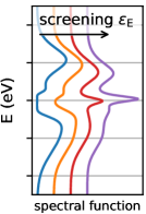
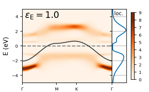
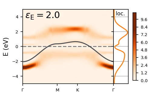
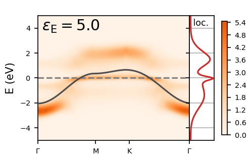
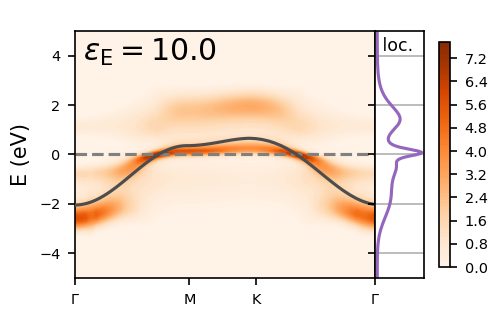
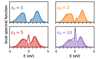
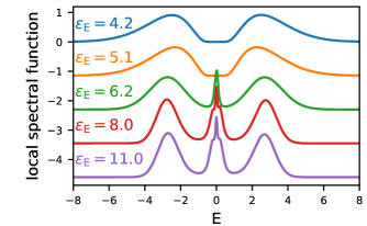
Figure 2 shows how the spectral function evolves from (the freestanding monolayer) to (encapsulation in bulk Si would correspond to ). The colored curve on the right of each graph shows the local density of states, which is the integral of the spectral function over the Brillouin Zone. The screening by the environment leads to substantial changes in the spectral function. Most dramatically, the system changes from an insulator to a metal. A comparison of and shows that the gap at the Fermi level disappears and a quasiparticle band emerges at the Fermi level. This is clearly visible both in the spectral function and the local density of states. Experimentally, the latter can be investigated using scanneling tunneling spectroscopy (STS). Below the Fermi level, the momentum-resolved spectral function can be investigated with angular resolved photo-emission spectroscopy (ARPES).
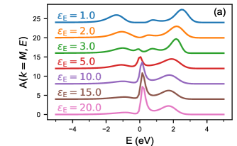
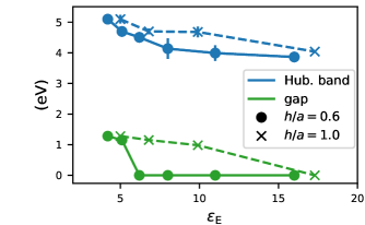
Spectral fingerprints of the Coulomb engineering are visible even without crossing the insulator-metal transition: a comparison of and shows that the size of the gap within the insulating phase is reduced by the screening. On the metallic side of the transition, the Hubbard side bands are still visible in the spectra and we can trace how their energy changes due to Coulomb engineering. To get a better view, Figure 3(a) shows the Energy Distribution Curves (EDCs, the cross-sections of the spectral function at fixed momentum) at . Both the lower and upper Hubbard band move towards the Fermi level as increases, and for a quasiparticle peak close to the Fermi level is visible. In addition to the changing position of the peaks, the Figure also clearly shows the spectral weight transfer to the quasiparticle peak at the expense of the Hubbard bands.
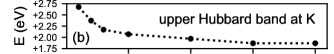
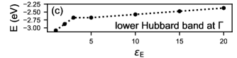
The Coulomb engineering of Mott insulators leads to eV-sized changes in peak positions, as shown in Figure 3(b,c). There, the peak position of the upper and lower Hubbard bands is shown. This energy has been extracted from the EDCs at and , corresponding to the bottom and top of the band. The environmental screening changes the position of the Hubbard bands by as much as 0.8 eV. The largest changes occur for small .
Inside the metallic phase at large , the effects of environmental screening are also visible in the quasiparticle band, close to the Fermi energy. The spectral weight in this band increases, as was visible in the local spectral function. In addition, the effective electron mass (see “Methods”) is reduced from at to at .
.3 Role of temperature
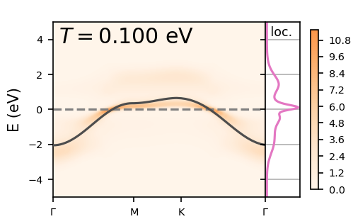
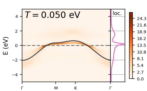
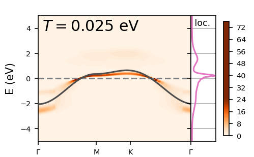
The spectral functions of Fig. 2 correspond to an electronic temperature of eV (1160 K). This temperature is obviously rather high for experiments, however we should stress that we are only simulating the electronic problem, where the energy scale is set by the bandwidth eV. The electronic temperature is small compared to this bandwidth. On the other hand, the typical energy scale for magnetic phenomena is much lower. Our calculations become substantially more difficult and expensive for lower temperatures, limiting the range where we can perform meaningful calculations. For , the screening is already quite effective, making the system less correlated, and this reduces the computational cost and allows us to reach lower temperatures. The spectra at reduced temperatures of eV (580 K) and eV (290 K, room temperature) are shown in Figure 4. The overall shape of the spectral function does not change substantially in this temperature range, the main difference is that spectral features become sharper at low temperature. The bandwidth sets the scale for the temperatures, for a system like magic-angle twisted bilayer graphene, where the bandwidth is two orders of magnitude smaller, our calculations would correspond to meV temperatures (10 K) and all gaps and changes in gaps are also on the meV-scale.
.4 Substrate
So far, we have considered the set-up of Fig. 1, a monolayer surrounded on both sides by a dielectric environment. Another experimentally relevant scenario is a Mott monolayer on a dielectric substrate with vacuum on the other side. In that case, the screened Coulomb interaction is given by equation (2). Figure 5 shows the resulting density of states (filled curves) in comparison with two-sided screening (lines). The starting point is the same, it corresponds to vacuum on both sides. As increases, the one-sided screening is less efficient and the resulting spectra retain more Mottish features (smaller quasiparticle peak, Hubbard bands). Still, the overall physics remains the same and Coulomb engineering across the insulator-metal transition is possible. This shows that experiments can use substrate screening instead of both sided screening when it is more convenient.
.5 Not just about
| (eV) | (eV) | (eV) | (eV) | |
|---|---|---|---|---|
| 1 | 4.19 | 1.88 | 1.20 | 1.07 |
| 2 | 3.51 | 1.32 | 0.76 | 0.67 |
| 5 | 2.77 | 0.76 | 0.36 | 0.31 |
| 10 | 2.38 | 0.49 | 0.19 | 0.16 |
Internal screening in (quasi-)two-dimensional materials is frequently incomplete, leading to substantial intersite Coulomb interactions Wehling et al. (2011); Hirayama et al. (2019), as shown in table 1 for the present model. Environmental screening changes the relative magnitudes of the on-site and intersite Coulomb matrix elements. The influence of intersite interactions on the electronic properties is determined by the spatial extent of charge excitations Schüler et al. (2013): only short-ranged (on-site and nearest-neighbour) interactions are relevant sufficiently deep in the insulating phase, whereas larger interaction lengths are important for the delocalized electrons in a metal. The crux here is that Coulomb engineering pushes the system across the boundary between the two distinct screening regimes, insulator and metal. Thus, screening in both phases has to be captured appropriately and consistently in a single theoretical description, necessitating advanced theoretical techniques such as the diagrammatic extensions of DMFT used here.
Discussion
After this computational demonstration of Coulomb engineering and its spectral fingerprints, we analyse qualitatively how the relevant parameters and scales enter, to guide experimental realizations. The effective height of the monolayer determines the length and momentum scale where the environment becomes important. For the limit of large , Equation (1) reduces to a two-dimensional Coulomb interaction with dielectric constant . In other words, on short length scales the interaction is exclusively determined by the monolayer. The relevant dimensionless parameter is , the ratio between the height of the monolayer and the in-plane lattice constant. For the Coulomb engineering to be efficient, should not be large. This is confirmed by +DMFT calculations, as described in the “Methods” section.
The control parameter in our study is , the dielectric constant of the environment. This means that the environment should not influence the monolayer in other ways such as hybridization or (pseudo)doping Shao et al. (2019), or the bandwidth widening that occurs in, e.g., strontium iridate superlattices Kim et al. (2017).
The internal dielectric constant of the monolayer sets the scale for , as the expression for shows. Typical values of range from 1 for vacuum, via 3.9 for SiO2 Robertson (2004) to 12 for Si Sze and Ng (2006). If is large, i.e., if screening inside the monolayer is already very effective, then much larger changes in the dielectric environment are needed to change . For the possibility to turn an insulator into a metal, the monolayer material itself should be an insulator and not too far way from the metallic state. If the goal is only to change the size of the Mott gap then the original material can be deeper inside the Mott phase.
The Hubbard interaction between electrons on the same site can serve as a useful indicator for the screening possibilities, when we compare a freestanding monolayer () and the corresponding bulk material (). For the (supposed) Mott insulator CrI3, the Hubbard interaction is reduced from eV for the monolayer to eV for the bulk Jang et al. (2019). For the strongly correlated metal SrVO3 there is a reduction from – eV in the monolayer to eV in the bulk Zhong et al. (2015). These substantial reductions of the Coulomb interaction are achieved by replacing vacuum with other Mott layers, meaning that a more effective dielectric environment will reduce the Coulomb interaction even more.
Meanwhile, the interlayer spacing and in-plane lattice constants in CrI3 are both approximately 7 Å so that Sivadas et al. (2018). Layered cuprate materials, another material family known for strong correlation physics, is worse in this respect, with typical values Murphy et al. (1987) of Å and Å, so . While it is possible to exfoliate cuprate single layers Novoselov et al. (2005), their thickness compared to the lattice constant renders Coulomb engineering more challenging. For transition metal dichalcogenides, can be achieved Al-Hilli and Evans (1972), which is better than the cuprates but not as good as CrI3.
It is even possible to reach when is the size of an emergent superlattice which can be much larger than the interatomic distance of the underlying lattice. One example is twisted bilayer graphene Bistritzer and MacDonald (2011); Cao et al. (2018a, b) with a moiré superlattice hundreds of times larger than the graphene unit cell so that can become genuinely small. We should note that is quite large in twisted bilayer graphene Pizarro et al. (2019) and that the insulating state is not of the idealized Mott-Hubbard type but likely involves spontaneous symmetry breaking in the valley and spin degrees of freedom Lu et al. (2019); Sharpe et al. (2019); Jiang et al. (2019); Serlin et al. (2020). Correspondingly, the interpretation of first possible experimental reports Stepanov et al. (2020); Saito et al. (2020); Liu et al. (2021) of Coulomb engineering related effects in twisted bilayer graphene is intricate Pizarro et al. (2019); Goodwin et al. (2019).
A clearer situation appears for certain charge density wave phases in 2d materials: 1T-TaS2 Tosatti, E. and Fazekas, P. (1976); Fazekas and Tosatti (1979, 1980), NbSe2 and TaSe2 have so-called commensurate charge density waves with a star-of-David lattice reconstruction, the emergent scale is times the original lattice constant. The star-of-David reconstructed TaSe2 monolayer has a Mott gap of approximately 0.1 eV Chen et al. (2020), and lends itself as a natural candidate for the exploration of Coulomb engineering of Mott materials.
A final important point for experimental realizations is the specific shape and extent of the correlated orbitals. This is of relevance for the interaction when is small. Our modelling assumes that the charge density of the electronic orbitals is homogeneous on the scale of the unit cell. A Wannier function with radius will have an increased local interaction, whereas the interaction between electrons in different unit cells is less affected by the Wannier radius. As an example, an Ohno fit Ohno (1964), , to the on-site and nearest-neighbor interactions in cuprates Hirayama et al. (2019) gives , whereas the same Ohno model in graphene Schüler et al. (2013) gives . Since the dielectric screening is more efficient on longer length scales, Coulomb engineering is more favourable for materials with a larger Wannier radius.
I Conclusion
We have demonstrated that the dielectric environment can be used to control Mott insulating layered materials and that Coulomb engineering across the insulator-metal transition is possible. Our calculations show the spectroscopic fingerprints of Coulomb engineering, namely eV-scale movement of the Hubbard bands and the appearance of a quasiparticle band as the system turns metallic. Based on our modelling, we can identify necessary conditions for Coulomb engineering. To be effective, the dielectric environment should be close to the monolayer, while also avoiding other monolayer-environment couplings like pseudodoping and hybridization. Furthermore, the monolayer itself should not screen too strongly. A good indicator is if the Hubbard parameter is much larger for the monolayer than for the corresponding bulk material. Our results open a perspective for the fabrication of heterostructures by the application of dielectric covering on parts of a Mott monolayer. In this way, the environment can create local phase transitions in correlated materials: metallic paths in an otherwise insulating layer or the control of unconventional superconducting phases via the reduction of the effective interaction. The sharpness of these dielectrically controlled heterostructures is controlled by the electronic Green’s function Rösner et al. (2016), so in Mott insulators where the electrons are localized, heterostructures can be atomically sharp.
Methods
Dual Boson
The system is studied in the grand canonical ensemble with density fixed to half-filling. For our computations, we use the Dual Boson method Rubtsov et al. (2012) with the implementation described in Ref. van Loon et al., 2014. It consists of a self-consistency cycle to determine the optimal Anderson Impurity Model (AIM). In this cycle, we include vertex corrections to the susceptibility in the ladder approach to ensure that the susceptibility satisfies charge conservation at small momenta. This is important when dealing with long-ranged . When self-consistency has been reached, we calculate the spatial self-energy in the last iteration using the second-order diagram of Figure 2b from van Loon et al., 2014, which together with the AIM self-energy is used to determine the Green’s function and finally the spectral function . The diagrammatic calculations are done on a periodic lattice, sufficient to rule out electronic finite-size effects, especially since the electrons are rather localized in the regime studied here. We study the non-magnetic insulator-metal transition, we do not allow for magnetic order in our calculations. The Anderson Impurity Model is solved using the ALPS/w2dynamics (for +DMFT, see below) CT-HYB solvers Bauer et al. (2011); Hafermann et al. (2013); Hafermann (2014); Wallerberger et al. (2019). All our calculations are done in Matsubara space, the analytical continuation to real energies is done to determine . For this, we use OmegaMaxEntBergeron and Tremblay (2016). To verify the reliability, we have also performed stochastic continuation using Spektra (https://spektra.app) Ghanem (2017); Ghanem and Koch (2020) for a representative subset of our calculations.
Effective mass
In the metallic phase, the effective electronic mass is a useful indicator of the strength of correlations. The effective mass renormalization consists of two parts Tomczak et al. (2014); Schäfer et al. (2015), a dynamical contribution and a static contribution. The dynamical contribution decreases as the Coulomb interaction is reduced by screening, but the spatial contribution actually increases due to Fock-like band widening. The latter effect turns out to be smaller, leading to an overall decrease of the effective mass upon increased screening. The values of the effective mass given in the Results section were determined on the -M high symmetry line, at the Fermi surface crossing. In our calculations, the effective mass depends only weakly on momentum.
+DMFT
To illustrate that our findings are representative of Mott monolayers in general, we have also performed +DMFT Biermann et al. (2003) calculations for a square lattice system, based on the implementation of Ref. Schäfer et al. (2015); Tomczak et al. (2017). The non-local contributions of the self-energy, calculated in a single-shot GW calculation, are added to the local DMFT self-energy Wallerberger et al. (2019).
The +DMFT treatment of the interaction in this model was restricted to local () and nearest-neighbor () terms. To make a comparison with the dielectric model of equation (1), we map the model onto the two-parameter effective interaction via two constraints:
| (4) | ||||
| (5) |
The first constraint ensures that the overall magnitude of the interaction is the same in the effective model, which is important for the Mott physics, the second constraint that the potential energy cost of checkerboard charge-density waves is equal for both interactions. The latter is important to ensure that the effective model is not biased towards the CDW phase of the square lattice extended Hubbard model Hansmann et al. (2013). For the material parameters, we used Å, and both and . The hopping was set to eV, the temperature to eV (290 K, room temperature).
The numerical advantage of the +DMFT approach compared to the Dual Boson method is that it does not involve so-called vertex corrections, which makes it substantially cheaper and allows us to explore larger parts of phase space even at low temperatures. Here, we use it to study the effect of . At the same time, the neglect of vertex corrections is an approximation, which is potentially problematic for collective excitations on longer length scales. This is why we cut off the interaction after the nearest-neighbors in this model. The square lattice at half-filling has particle-hole symmetry, for the present investigation this, for example, means that the lower and upper Hubbard band should appear at the same (absolute) energy, which is used to estimate the error bars in figure 6, coming from uncertainty in the analytical continuation.
The results are shown in figures 6 and 7. As in the Dual Boson results, the induced insulator-metal transition is clearly visible. Here, this transition occurs around for and for . As increases, the Hubbard bands move towards the Fermi surface.
Acknowledgements.
The authors thank P. Hofmann for useful discussions and K. Ghanem for the help with the stochastic continuation. The authors acknowledge the North-German Supercomputing Alliance (HLRN) for providing computing resources via project number hbp00047 that have contributed to the research results reported in this paper. D. S. and J. M. T. acknowledge support by the Austrian Science Fund (FWF) through project ’LinReTraCe’ P 30213-N36. Some calculations were performed on the Vienna Scientific Cluster (VSC). G. S. acknowledges financial support from the DFG through the Würzburg-Dresden Cluster of Excellence on Complexity and Topology in Quantum Matter – ct.qmat (EXC 2147, project-id 39085490). T.W. acknowledges support from the DFG through QUAST (FOR 5249, No. 449872909) and via the Cluster of Excellence “CUI: Advanced Imaging of Matter” (EXC 2056, No. 390715994).Author contributions
EvL performed the Dual Boson calculations, MS performed the analytical continuations, DS and JMT performed the +DMFT calculations. All authors contributed to the interpretation of the results and to the writing of the manuscript.
References
- Jena and Konar (2007) Debdeep Jena and Aniruddha Konar, “Enhancement of carrier mobility in semiconductor nanostructures by dielectric engineering,” Phys. Rev. Lett. 98, 136805 (2007).
- Rösner et al. (2016) M. Rösner, C. Steinke, M. Lorke, C. Gies, F. Jahnke, and T. O. Wehling, “Two-dimensional heterojunctions from nonlocal manipulations of the interactions,” Nano Letters 16, 2322–2327 (2016), pMID: 26918626.
- Raja et al. (2017) Archana Raja, Andrey Chaves, Jaeeun Yu, Ghidewon Arefe, Heather M Hill, Albert F Rigosi, Timothy C Berkelbach, Philipp Nagler, Christian Schüller, Tobias Korn, et al., “Coulomb engineering of the bandgap and excitons in two-dimensional materials,” Nature communications 8, 15251 (2017).
- Qiu et al. (2017) Diana Y. Qiu, Felipe H. da Jornada, and Steven G. Louie, “Environmental screening effects in 2d materials: Renormalization of the bandgap, electronic structure, and optical spectra of few-layer black phosphorus,” Nano Letters 17, 4706–4712 (2017), pMID: 28677398.
- Radisavljevic and Kis (2013) Branimir Radisavljevic and Andras Kis, “Mobility engineering and a metal–insulator transition in monolayer MoS2,” Nature materials 12, 815 (2013).
- Borghardt et al. (2017) Sven Borghardt, Jhih-Sian Tu, Florian Winkler, Jürgen Schubert, Willi Zander, Kristjan Leosson, and Beata E. Kardynał, “Engineering of optical and electronic band gaps in transition metal dichalcogenide monolayers through external dielectric screening,” Phys. Rev. Materials 1, 054001 (2017).
- Papić et al. (2011) Z. Papić, R. Thomale, and D. A. Abanin, “Tunable electron interactions and fractional quantum hall states in graphene,” Phys. Rev. Lett. 107, 176602 (2011).
- Lin et al. (2014) Yuxuan Lin, Xi Ling, Lili Yu, Shengxi Huang, Allen L. Hsu, Yi-Hsien Lee, Jing Kong, Mildred S. Dresselhaus, and Tomás Palacios, “Dielectric screening of excitons and trions in single-layer MoS2,” Nano Letters 14, 5569–5576 (2014), pMID: 25216267.
- Gupta et al. (2017) Garima Gupta, Sangeeth Kallatt, and Kausik Majumdar, “Direct observation of giant binding energy modulation of exciton complexes in monolayer ,” Phys. Rev. B 96, 081403 (2017).
- Drüppel et al. (2017) Matthias Drüppel, Thorsten Deilmann, Peter Krüger, and Michael Rohlfing, “Diversity of trion states and substrate effects in the optical properties of an MoS2 monolayer,” Nature communications 8, 2117 (2017).
- Florian et al. (2018) Matthias Florian, Malte Hartmann, Alexander Steinhoff, Julian Klein, Alexander W. Holleitner, Jonathan J. Finley, Tim O. Wehling, Michael Kaniber, and Christopher Gies, “The dielectric impact of layer distances on exciton and trion binding energies in van der Waals heterostructures,” Nano Letters 18, 2725–2732 (2018), pMID: 29558797.
- Steinleitner et al. (2018) Philipp Steinleitner, Philipp Merkl, Alexander Graf, Philipp Nagler, Kenji Watanabe, Takashi Taniguchi, Jonas Zipfel, Christian Schüller, Tobias Korn, Alexey Chernikov, Samuel Brem, Malte Selig, Gunnar Berghäuser, Ermin Malic, and Rupert Huber, “Dielectric engineering of electronic correlations in a van der Waals heterostructure,” Nano Letters 18, 1402–1409 (2018), pMID: 29365262.
- Park et al. (2018) Soohyung Park, Niklas Mutz, Thorsten Schultz, Sylke Blumstengel, Ali Han, Areej Aljarb, Lain-Jong Li, Emil J W List-Kratochvil, Patrick Amsalem, and Norbert Koch, “Direct determination of monolayer MoS2 and WSe2 exciton binding energies on insulating and metallic substrates,” 2D Materials 5, 025003 (2018).
- Jia et al. (2019) Guang Yi Jia, Yan Zhou, Yong Zheng Niu, Shu Bin Huang, and Yan Peng Cao, “Screening effect of ultrathin gold films on excitons in monolayer WS2,” Plasmonics (2019), 10.1007/s11468-018-00894-6.
- Utama et al. (2019) M Iqbal Bakti Utama, Hans Kleemann, Wenyu Zhao, Chin Shen Ong, H Felipe, Diana Y Qiu, Hui Cai, Han Li, Rai Kou, Sihan Zhao, et al., “A dielectric-defined lateral heterojunction in a monolayer semiconductor,” Nature Electronics 2, 60 (2019).
- Waldecker et al. (2019) Lutz Waldecker, Archana Raja, Malte Rösner, Christina Steinke, Aaron Bostwick, Roland J. Koch, Chris Jozwiak, Takashi Taniguchi, Kenji Watanabe, Eli Rotenberg, Tim O. Wehling, and Tony F. Heinz, “Rigid band shifts in two-dimensional semiconductors through external dielectric screening,” Phys. Rev. Lett. 123, 206403 (2019).
- Stepanov et al. (2020) Petr Stepanov, Ipsita Das, Xiaobo Lu, Ali Fahimniya, Kenji Watanabe, Takashi Taniguchi, Frank HL Koppens, Johannes Lischner, Leonid Levitov, and Dmitri K Efetov, “Untying the insulating and superconducting orders in magic-angle graphene,” Nature 583, 375–378 (2020).
- Saito et al. (2020) Yu Saito, Jingyuan Ge, Kenji Watanabe, Takashi Taniguchi, and Andrea F Young, “Independent superconductors and correlated insulators in twisted bilayer graphene,” Nature Physics 16, 926–930 (2020).
- Liu et al. (2021) Xiaoxue Liu, Zhi Wang, K. Watanabe, T. Taniguchi, Oskar Vafek, and J. I. A. Li, “Tuning electron correlation in magic-angle twisted bilayer graphene using coulomb screening,” Science 371, 1261–1265 (2021).
- Schönhoff et al. (2016) G. Schönhoff, M. Rösner, R. E. Groenewald, S. Haas, and T. O. Wehling, “Interplay of screening and superconductivity in low-dimensional materials,” Phys. Rev. B 94, 134504 (2016).
- Imada et al. (1998) Masatoshi Imada, Atsushi Fujimori, and Yoshinori Tokura, “Metal-insulator transitions,” Rev. Mod. Phys. 70, 1039–1263 (1998).
- Emelyanenko and Boinovich (2008) Alexandre Emelyanenko and Ludmila Boinovich, “On the effect of discrete charges adsorbed at the interface on nonionic liquid film stability: charges in the film,” Journal of Physics: Condensed Matter 20, 494227 (2008).
- Rösner et al. (2015) M. Rösner, E. Şaşıoğlu, C. Friedrich, S. Blügel, and T. O. Wehling, “Wannier function approach to realistic Coulomb interactions in layered materials and heterostructures,” Phys. Rev. B 92, 085102 (2015).
- Katsnelson (2012) Mikhail I Katsnelson, Graphene: carbon in two dimensions (Cambridge University press, Cambridge, 2012).
- Aryasetiawan et al. (2004) F. Aryasetiawan, M. Imada, A. Georges, G. Kotliar, S. Biermann, and A. I. Lichtenstein, “Frequency-dependent local interactions and low-energy effective models from electronic structure calculations,” Phys. Rev. B 70, 195104 (2004).
- Al-Hilli and Evans (1972) A.A. Al-Hilli and B.L. Evans, “The preparation and properties of transition metal dichalcogenide single crystals,” Journal of Crystal Growth 15, 93 – 101 (1972).
- Georges et al. (1996) Antoine Georges, Gabriel Kotliar, Werner Krauth, and Marcelo J. Rozenberg, “Dynamical mean-field theory of strongly correlated fermion systems and the limit of infinite dimensions,” Rev. Mod. Phys. 68, 13–125 (1996).
- Kotliar et al. (2006) G. Kotliar, S. Y. Savrasov, K. Haule, V. S. Oudovenko, O. Parcollet, and C. A. Marianetti, “Electronic structure calculations with dynamical mean-field theory,” Rev. Mod. Phys. 78, 865–951 (2006).
- Rohringer et al. (2018) G. Rohringer, H. Hafermann, A. Toschi, A. A. Katanin, A. E. Antipov, M. I. Katsnelson, A. I. Lichtenstein, A. N. Rubtsov, and K. Held, “Diagrammatic routes to nonlocal correlations beyond dynamical mean field theory,” Rev. Mod. Phys. 90, 025003 (2018).
- Rubtsov et al. (2012) A. N. Rubtsov, M. I. Katsnelson, and A. I. Lichtenstein, “Dual boson approach to collective excitations in correlated fermionic systems,” Annals of Physics 327, 1320 (2012).
- van Loon et al. (2014) Erik G. C. P. van Loon, Alexander I. Lichtenstein, Mikhail I. Katsnelson, Olivier Parcollet, and Hartmut Hafermann, “Beyond extended dynamical mean-field theory: Dual boson approach to the two-dimensional extended hubbard model,” Phys. Rev. B 90, 235135 (2014).
- Biermann et al. (2003) S. Biermann, F. Aryasetiawan, and A. Georges, “First-principles approach to the electronic structure of strongly correlated systems: Combining the approximation and dynamical mean-field theory,” Phys. Rev. Lett. 90, 086402 (2003).
- Tomczak et al. (2017) J. M. Tomczak, P. Liu, A. Toschi, G. Kresse, and K. Held, “Merging with DMFT and non-local correlations beyond,” The European Physical Journal Special Topics 226, 2565–2590 (2017).
- Wehling et al. (2011) T. O. Wehling, E. Şaşıoğlu, C. Friedrich, A. I. Lichtenstein, M. I. Katsnelson, and S. Blügel, “Strength of effective Coulomb interactions in graphene and graphite,” Phys. Rev. Lett. 106, 236805 (2011).
- Hirayama et al. (2019) Motoaki Hirayama, Takahiro Misawa, Takahiro Ohgoe, Youhei Yamaji, and Masatoshi Imada, “Effective Hamiltonian for cuprate superconductors derived from multiscale ab initio scheme with level renormalization,” Phys. Rev. B 99, 245155 (2019).
- Schüler et al. (2013) M. Schüler, M. Rösner, T. O. Wehling, A. I. Lichtenstein, and M. I. Katsnelson, “Optimal Hubbard models for materials with nonlocal Coulomb interactions: Graphene, silicene, and benzene,” Phys. Rev. Lett. 111, 036601 (2013).
- Shao et al. (2019) Bin Shao, Andreas Eich, Charlotte Sanders, Arlette S Ngankeu, Marco Bianchi, Philip Hofmann, Alexander A Khajetoorians, and Tim O Wehling, “Pseudodoping of a metallic two-dimensional material by the supporting substrate,” Nature communications 10, 180 (2019).
- Kim et al. (2017) Bongjae Kim, Peitao Liu, and Cesare Franchini, “Dimensionality-strain phase diagram of strontium iridates,” Phys. Rev. B 95, 115111 (2017).
- Robertson (2004) J Robertson, “High dielectric constant oxides,” The European Physical Journal-Applied Physics 28, 265–291 (2004).
- Sze and Ng (2006) Simon M Sze and Kwok K Ng, Physics of semiconductor devices (John Wiley & Sons, 2006).
- Jang et al. (2019) Seung Woo Jang, Min Yong Jeong, Hongkee Yoon, Siheon Ryee, and Myung Joon Han, “Microscopic understanding of magnetic interactions in bilayer ,” Phys. Rev. Materials 3, 031001 (2019).
- Zhong et al. (2015) Zhicheng Zhong, Markus Wallerberger, Jan M. Tomczak, Ciro Taranto, Nicolaus Parragh, Alessandro Toschi, Giorgio Sangiovanni, and Karsten Held, “Electronics with correlated oxides: as a mott transistor,” Phys. Rev. Lett. 114, 246401 (2015).
- Sivadas et al. (2018) Nikhil Sivadas, Satoshi Okamoto, Xiaodong Xu, Craig. J. Fennie, and Di Xiao, “Stacking-dependent magnetism in bilayer CrI3,” Nano Letters 18, 7658–7664 (2018), pMID: 30408960.
- Murphy et al. (1987) D. W. Murphy, S. Sunshine, R. B. van Dover, R. J. Cava, B. Batlogg, S. M. Zahurak, and L. F. Schneemeyer, “New superconducting cuprate perovskites,” Phys. Rev. Lett. 58, 1888–1890 (1987).
- Novoselov et al. (2005) K. S. Novoselov, D. Jiang, F. Schedin, T. J. Booth, V. V. Khotkevich, S. V. Morozov, and A. K. Geim, “Two-dimensional atomic crystals,” Proceedings of the National Academy of Sciences 102, 10451–10453 (2005).
- Bistritzer and MacDonald (2011) Rafi Bistritzer and Allan H. MacDonald, “Moiré bands in twisted double-layer graphene,” Proceedings of the National Academy of Sciences 108, 12233–12237 (2011).
- Cao et al. (2018a) Yuan Cao, Valla Fatemi, Shiang Fang, Kenji Watanabe, Takashi Taniguchi, Efthimios Kaxiras, and Pablo Jarillo-Herrero, “Unconventional superconductivity in magic-angle graphene superlattices,” Nature 556, 43 (2018a).
- Cao et al. (2018b) Yuan Cao, Valla Fatemi, Ahmet Demir, Shiang Fang, Spencer L Tomarken, Jason Y Luo, Javier D Sanchez-Yamagishi, Kenji Watanabe, Takashi Taniguchi, Efthimios Kaxiras, et al., “Correlated insulator behaviour at half-filling in magic-angle graphene superlattices,” Nature 556, 80 (2018b).
- Pizarro et al. (2019) J. M. Pizarro, M. Rösner, R. Thomale, R. Valentí, and T. O. Wehling, “Internal screening and dielectric engineering in magic-angle twisted bilayer graphene,” Phys. Rev. B 100, 161102 (2019).
- Lu et al. (2019) Xiaobo Lu, Petr Stepanov, Wei Yang, Ming Xie, Mohammed Ali Aamir, Ipsita Das, Carles Urgell, Kenji Watanabe, Takashi Taniguchi, Guangyu Zhang, et al., “Superconductors, orbital magnets and correlated states in magic-angle bilayer graphene,” Nature 574, 653–657 (2019).
- Sharpe et al. (2019) Aaron L Sharpe, Eli J Fox, Arthur W Barnard, Joe Finney, Kenji Watanabe, Takashi Taniguchi, MA Kastner, and David Goldhaber-Gordon, “Emergent ferromagnetism near three-quarters filling in twisted bilayer graphene,” Science 365, 605–608 (2019).
- Jiang et al. (2019) Yuhang Jiang, Xinyuan Lai, Kenji Watanabe, Takashi Taniguchi, Kristjan Haule, Jinhai Mao, and Eva Y Andrei, “Charge order and broken rotational symmetry in magic-angle twisted bilayer graphene,” Nature 573, 91–95 (2019).
- Serlin et al. (2020) M Serlin, CL Tschirhart, H Polshyn, Y Zhang, J Zhu, K Watanabe, T Taniguchi, L Balents, and AF Young, “Intrinsic quantized anomalous hall effect in a moiré heterostructure,” Science 367, 900–903 (2020).
- Goodwin et al. (2019) Zachary A. H. Goodwin, Fabiano Corsetti, Arash A. Mostofi, and Johannes Lischner, “Twist-angle sensitivity of electron correlations in moiré graphene bilayers,” Phys. Rev. B 100, 121106 (2019).
- Tosatti, E. and Fazekas, P. (1976) Tosatti, E. and Fazekas, P., “On the nature of the low-temperature phase of 1T-TaS2,” J. Phys. Colloques 37, C4–165–C4–168 (1976).
- Fazekas and Tosatti (1979) P. Fazekas and E. Tosatti, “Electrical, structural and magnetic properties of pure and doped 1T-TaS2,” Philosophical Magazine B 39, 229–244 (1979).
- Fazekas and Tosatti (1980) P. Fazekas and E. Tosatti, “Charge carrier localization in pure and doped 1T-TaS2,” Physica B+C 99, 183 – 187 (1980).
- Chen et al. (2020) Yi Chen, Wei Ruan, Meng Wu, Shujie Tang, Hyejin Ryu, Hsin-Zon Tsai, Ryan L Lee, Salman Kahn, Franklin Liou, Caihong Jia, et al., “Strong correlations and orbital texture in single-layer 1T-TaSe2,” Nature Physics 16, 218–224 (2020).
- Ohno (1964) Kimio Ohno, “Some remarks on the Pariser-Parr-Pople method,” Theoretica chimica acta 2, 219–227 (1964).
- Bauer et al. (2011) B Bauer, L D Carr, H G Evertz, A Feiguin, J Freire, S Fuchs, L Gamper, J Gukelberger, E Gull, S Guertler, A Hehn, R Igarashi, S V Isakov, D Koop, P N Ma, P Mates, H Matsuo, O Parcollet, G Pawłowski, J D Picon, L Pollet, E Santos, V W Scarola, U Schollwöck, C Silva, B Surer, S Todo, S Trebst, M Troyer, M L Wall, P Werner, and S Wessel, “The ALPS project release 2.0: open source software for strongly correlated systems,” Journal of Statistical Mechanics: Theory and Experiment 2011, P05001 (2011).
- Hafermann et al. (2013) Hartmut Hafermann, Philipp Werner, and Emanuel Gull, “Efficient implementation of the continuous-time hybridization expansion quantum impurity solver,” Computer Physics Communications 184, 1280 – 1286 (2013).
- Hafermann (2014) Hartmut Hafermann, “Self-energy and vertex functions from hybridization-expansion continuous-time quantum monte carlo for impurity models with retarded interaction,” Phys. Rev. B 89, 235128 (2014).
- Wallerberger et al. (2019) Markus Wallerberger, Andreas Hausoel, Patrik Gunacker, Alexander Kowalski, Nicolaus Parragh, Florian Goth, Karsten Held, and Giorgio Sangiovanni, “w2dynamics: Local one- and two-particle quantities from dynamical mean field theory,” Computer Physics Communications 235, 388 – 399 (2019).
- Bergeron and Tremblay (2016) Dominic Bergeron and A.-M. S. Tremblay, “Algorithms for optimized maximum entropy and diagnostic tools for analytic continuation,” Phys. Rev. E 94, 023303 (2016).
- Ghanem (2017) Khaldoon Ghanem, Stochastic Analytic Continuation: A Bayesian Approach, Dissertation, RWTH Aachen University (2017), dissertation, RWTH Aachen University, 2017.
- Ghanem and Koch (2020) Khaldoon Ghanem and Erik Koch, “Average spectrum method for analytic continuation: Efficient blocked-mode sampling and dependence on the discretization grid,” Phys. Rev. B 101, 085111 (2020).
- Tomczak et al. (2014) Jan M. Tomczak, M. Casula, T. Miyake, and S. Biermann, “Asymmetry in band widening and quasiparticle lifetimes in : Competition between screened exchange and local correlations from combined and dynamical mean-field theory ,” Phys. Rev. B 90, 165138 (2014).
- Schäfer et al. (2015) T. Schäfer, A. Toschi, and Jan M. Tomczak, “Separability of dynamical and nonlocal correlations in three dimensions,” Phys. Rev. B 91, 121107 (2015).
- Hansmann et al. (2013) P. Hansmann, T. Ayral, L. Vaugier, P. Werner, and S. Biermann, “Long-range coulomb interactions in surface systems: A first-principles description within self-consistently combined and dynamical mean-field theory,” Phys. Rev. Lett. 110, 166401 (2013).