Highly efficient spin orbit torque in Pt/Co/Ir multilayers with antiferromagnetic interlayer exchange coupling
Abstract
We have studied the spin orbit torque (SOT) in Pt/Co/Ir multilayers with 3 repeats of the unit structure. As the system exhibits oscillatory interlayer exchange coupling (IEC) with varying Ir layer thickness, we compare the SOT of films when the Co layers are coupled ferromagnetically and antiferromagnetically. SOT is evaluated using current induced shift of the anomalous Hall resistance hysteresis loops. A relatively thick Pt layer, serving as a seed layer to the multilayer, is used to generate spin current via the spin Hall effect. In the absence of antiferromagnetic coupling, the SOT is constant against the applied current density and the corresponding spin torque efficiency (i.e. the effective spin Hall angle) is 0.09, in agreement with previous reports. In contrast, for films with antiferromagnetic coupling, the SOT increases with the applied current density and eventually saturates. The SOT at saturation is a factor of 15 larger than that without the antiferromagnetic coupling. The spin torque efficiency is 5 times larger if we assume the net total magnetization is reduced by a factor of 3 due to the antiferromagnetic coupling. Model calculations based on the Landau Lifshitz Gilbert equation show that the presence of antiferromagnetic coupling can increase the SOT but the degree of enhancement is limited, in this case, to a factor of 1.2-1.4. We thus consider there are other sources of SOT, possibly at the interfaces, which may account for the highly efficient SOT in the uncompensated synthetic anti-ferromagnet (SAF) multilayers.
I Introduction
Spin orbit torque (SOT)Manchon and Zhang (2009) is considered as a viable means to manipulate magnetization of thin magnetic layers for next generation magnetic random access memories (MRAM)Garello et al. (2018). Bilayers consisting of a non-magnetic metal (NM) and a ferromagnetic metal (FM) are widely used as a prototypeMiron et al. (2011); Liu et al. (2012) to demonstrate the feasibility of SOT technologies. The spin torque efficiency is often defined as a parameter that characterizes both the degree of spin current generated from the NM layer and the effectiveness of the spin current to exert spin torque on the magnetic moments of the FM layer. For a spin transparent NM/FM interface, the spin torque efficiency is equivalent to the spin Hall angle of the NM layer.
To improve the spin torque efficiency, significant effort has been put forward to explore materials with large spin Hall angle. Beyond the 5d transition metals, recent studies have shown that topological insulatorsMellnik et al. (2014); Fan et al. (2014), van der Waals materialsMacNeill et al. (2017) and antiferromagnets exhibit large spin torque efficiency. In particular, antiferromagnetic materials are attracting interest as an efficient spin current source which are readily accessibleZhang et al. (2014, 2016). Recent experiments have demonstrated current controlled magnetization switching of ferromagnetic layer using antiferromagnetic thin films as the spin current sourceFukami et al. (2016). In addition to the conventional intrinsic and extrinsic spin Hall effects, antiferromagnetic materials may have additional means to generate spin current due to their unique magnetic structureChen et al. (2014); Zhang et al. (2017). The large anomalous Hall effectNakatsuji et al. (2015); Nayak et al. (2016) and the spin Hall effectZhang et al. (2016) in chiral antiferromagnets are known as a consequence of electrons acquiring Berry’s phase as they travel through the magnetic texture.
Collinear antiferromagnetsDuine et al. (2018) can be designed by means of interlayer exchange coupling (IEC) of thin ferromagnetic layersParkin et al. (1990). As the net magnetic moment can be reduced to near zero, such synthetic anti-ferromagnets (SAF) play an essential role in modern MRAM technologies: they are typically used as the magnetic reference layer owing to their negligible stray fieldParkin et al. (1999). The small net magnetization is also attractive with regard to their use as the information recording layer (i.e. free layer). As the current needed to control the magnetization direction of the free layer scales with its saturation magnetization , smaller is desirable for low power operation provided that one can keep the thermal stability factor sufficiently high. Recent studies have shown that the efficiency to manipulate the magnetization direction of ferrimagnets or synthetic antiferromagnets using spin orbit torques can be significantly increased when the net magnetization, or the net angular momentum, of such magnets is reduced to near zeroRoschewsky et al. (2016); Finley and Liu (2016); Mishra et al. (2017); Ueda et al. (2017); Zhang et al. (2018); Krishnia et al. (2019). Similarly, the velocity of magnetic domain walls driven by fieldKim et al. (2017) or currentYang et al. (2015); Caretta et al. (2018) can be enhanced when the net angular momentum or magnetization is minimized.
Here we compare spin orbit torque switching of Pt/Co/Ir multilayers with ferromagnetic and antiferromagnetic interlayer exchange coupling. We use multilayers consisting of three repeats of the unit structure Pt/Co/Ir: the film is an uncompensated SAF with a non-zero net magnetization if the three Co layers are coupled antiferromagnetically. A relatively thick Pt layer, serving as a seed layer to the multilayer, is used to generate spin current via the spin Hall effect. The SOT of the uncompensated SAF is nearly 15 times larger than that when the Co layers are coupled ferromagnetically. The spin torque efficiency is 5 times larger for the former if we assume the net total magnetization is 3 times smaller for the antiferromagnetically coupled state, although the dominant SOT may be exerted at the bottom Co layer in contact with the Pt seed layer. We model the system to study possible mechanisms that can cause such large enhancement of SOT due to antiferromagnetic IEC.
II Experimental setup
Multilayers composed of Sub./3 Ta/2 Pt/[0.6 Pt/0.9 Co/ Ir]3×/2 MgO/1 Ta (units in nanometer) were grown on Si substrates with SiO2 coating (thickness: 100 nm) using radio frequency magnetron sputtering. The thickness of the Ir layer (0.1 nm1.1 nm) was varied across the substrate using a moving shutter during the deposition process. Optical lithography and Ar ion milling were used to form a Hall-bar. Schematic of the experimental setup and definition of the coordinate axis are shown in Fig. 1(b). The width of the wire and the distance between the longitudinal voltage probes are 10 m and 25 m, respectively. DC current () was passed along the axis. Positive current is defined as current flow to . The Hall resistance () is obtained by dividing the measured Hall voltage () with the current supplied, i.e. .
III Results and discussion
III.1 Film characteristics
Figure 1(a) shows the out-of-plane field () dependence of the Hall resistance () for films with various Ir layer thicknesses. In this thickness range (0.1 nm 1.1 nm), oscillatory interlayer exchange coupling is observed: the coupling is either ferromagnetic (F) or antiferromagnetic (AF). For the films with F coupling, the hysteresis loops show two stable states corresponding to the three Co layers’ magnetization all pointing along (from top to bottom, the Co layers’ magnetization are ) and -z (). For such coupling, the three Co layers switch together at the same field. In contrast, we typically find four stable states for the films with AF coupling: the four states correspond to two saturated states ( and ) and two intermediate states with the middle Co layer magnetization pointing against that of the two neighboring layers ( and ). See the arrows displayed in Fig. 1(a) for the corresponding magnetization configuration of the four states. The field at which switching between the parallel to antiparallel states occurs is defined as , as schematically defined in Fig. 1(a). Note that the hysteresis loop of the film with 1.1 nm indicates that the AF coupling is in place but weak such that the field range which the antiparallel states appear is small.
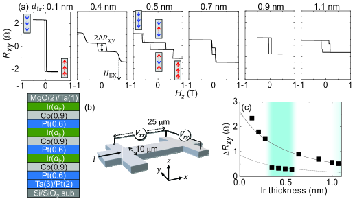
Figure 1(c) shows the Ir layer thickness () dependence of the anomalous Hall resistance . is defined as the difference of for the two metastable states at zero-field, i.e. at remanence. decreases with increasing due to current shunting into the Ir layer. The blue shaded regions in Fig. 1(c) display the Ir thickness range in which the AF coupled state is stable. To study the magnetic configuration of the films at remanence via the anomalous Hall resistance, we model the transport properties of the heterostructure assuming current flow within the highly conducting Pt, Co and Ir layers. Current flow into the Ta seed layer, which has a significantly larger resistivity than the conducting layers, is neglected. Note that the MgO/Ta capping layer does not conduct current (the top Ta layer is oxidized and forms an insulator). We define the resistivities (thickness) of the Pt, Co and Ir layers as, , respectively. Assuming a parallel circuit model, reads
| (1) |
where and is the effective anomalous Hall angle. We use Eq. (1) to characterize the results of the films with F- and AF-coupling. Assuming that the resistivity of the conducting layers is the same for the films with F- and AF-coupling, the difference in between the two can be attributed to the net magnetization along the axis, which is implicitly included in . The solid and dotted lines in Fig. 1(c) show the calculated , with of the dotted line being 1/3 of that of the solid line. These results are consistent with the picture that the remanent state of the films with AF coupling have net magnetization that is one third of that of the F coupling films.
III.2 Current induced torque
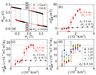
The current-induced shift of the hysteresis loops were used to estimate the spin torque efficiency of the multilayersPai et al. (2016). A constant bias field directed along the current flow () was applied while the Hall resistance was measured as a function of . Figure 2(a) shows exemplary - loops for a film with AF coupling (0.4 nm) when positive and negative currents were applied under a bias field 1 T. The two metastable states at zero field represent the antiferromagnetically coupled states and . When positive (negative) current is applied, the center of the hysteresis loop shifts to positive (negative) . The shift of the loop center with respect to =0 is defined as Pai et al. (2016). In the AF coupled films, we note that the current-induced shift of the hysteresis loops is nearly zero for the switching between the saturated states and the antiparallel states, i.e. transitions from to states, to states, and vice versa. Note that these switching takes place at larger compared to that between the antiparallel states ( to and vice versa). We therefore focus on the switching between the and the states.
Figure 2(b) shows the current density () dependence of for films with AF coupling (0.4 nm) and F coupling (0.3 nm). The in-plane bias field was set to 1 T for the former and 0.15 T for the latter. is obtained by dividing the current () with the width of the wire and the total thickness of the conducting Pt, Co and Ir layers: although the resistivities of the Pt, Co and Ir layers are different, we assume a uniform current flow within these layers for simplicity. As evident in Fig. 2(b), increases linearly with for the film with F coupling (open squares). In contrast, for the film with AF coupling (solid circles), increases abruptly above a threshold current density of A/m2. To obtain the spin torque efficiency, it is customary to divide with Pai et al. (2016). Figure 2(c) displays as a function of . is constant for all for the film with F coupling (open squares) whereas it saturates at A/m2 for the film with AF coupling (solid circles). Interestingly, the saturated value of for the latter (film with AF coupling) is significantly larger than the constant of the former (F coupling).
As the in-plane bias field () applied during the hysteresis loop measurements is different for the films with F and AF couplings, we study the dependence of . For single magnetic layer films (e.g. NM/FM bilayers), it is known that takes a constant value when the magnitude of is larger than that of the Dzyaloshinskii-Moriya (DM) exchange field : the constant for is proportional to the spin torque efficiency Pai et al. (2016). This is also the case for films with multiple magnetic layers coupled ferromagneticallyIshikuro et al. (2019). For multilayer films with AF coupling, here we show in Fig. 2(d) vs obtained using different for the film with nm. Although values of varies with when is smaller than the threshold current density, the saturated value of (above A/m2) is almost the same within the applied field () range. We thus take the upon saturation, defined as hereafter, as a measure of the spin torque efficiency for the films with AF coupling. For the films with F coupling, we assign as the constant when .
Note that the current-induced shift of the hysteresis loops for the films with AF coupling becomes near zero when 0.4 T, suggesting that lies between 0.4 T and 0.8 T ( nm). This is significantly larger than the of the multilayer films with F coupling reported previously ( T)Ishikuro et al. (2019). For the films with AF coupling, we consider the field required to cause saturation of , which has been assigned as previously, is related to the emergence of IEC. Experimentally, such saturation field correspond to needed to align the magnetization direction of all domain walls. If IEC is present in the system, the exchange coupling field acts on the domain walls, and thus it will take extra field to align their magnetization direction along . As is T to T, it is likely that the saturation field is dominated by .
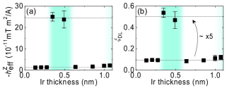
The Ir layer thickness dependence of is plotted in Fig. 3(a). The average for films with F (AF) coupling is 1.5 mT (25 mT) per current density of A/m2. To convert to the spin torque efficiency (), we use the relation (for )
| (2) |
where is the electric charge, is the reduced Planck constant, and is the total thickness of the magnetic layers. is the effective saturation magnetization of the system. Since the net magnetic moment of the films with AF coupling is one third of that of the films with F coupling, we substitute for the former and for the latter in Eq. (2). is the saturation magnetization of the Co layer which is estimated using magnetometry measurements. As slightly varies with Ishikuro et al. (2019), we interpolate the data to obtain the for the Hall bars studied here. Note that the dominant SOT likely takes place at the bottom Co layer which is in contact with the relatively thick Pt seed layer. It is not obvious if the spin current impinging on the bottom Co layer will see a three times reduced magnetization when the three Co layers are coupled antiferromagnetically. The use of for the films with AF coupling thus remains as an issue that need to be addressed. is plotted as a function of in Fig. 3(b). As evident, for the films with AF coupling is nearly five times larger than that of the films with F coupling, reaching a value of 0.5.
III.3 Model calculations
Previously it has been reported that the spin torque efficiency can be enhanced by using antiferromagnetically coupled magnetic layersMishra et al. (2017); Zhang et al. (2018). In particular, similar value of was reported in a completely compensated synthetic antiferromagnet, which was associated with the nearly zero net magnetic momentZhang et al. (2018). Here we find that the spin torque efficiency () is large even though the net magnetic moment is not zero. To account for these results, we study the effect of the so-called exchange coupling torqueYang et al. (2015); Mishra et al. (2017) on .
We first consider a NM/FM bilayer to which both the SOT and the external magnetic field are applied. Dynamics of the magnetization can be described using the Landau-Lifshitz-Gilbert equation:
| (3) |
where is the magnetization unit vector and is the Gilbert damping constant of the magnetic layer. is the gyromagnetic ratio, is the effective magnetic field that acts on . The effective field can be expressed as , where and are the saturation magnetization and the total energy of the system. is meant to take the functional derivative of with . The energy density takes the form
| (4) |
where is the volume of the magnetic layer, is the uniaxial perpendicular magnetic anisotropy energy density. and are the anisotropy field and the external field, respectively. The third term on the right hand side of Eq. (3) represents the spin orbit torque on . is a unit vector that represents the polarization of the spin current that diffuses into the magnetic layer and is the damping-like spin orbit effective field. We assume the current flows in the NM layer along the axis and generates a spin current with that diffuses into the magnetic layer (here we set such that it agrees with the spin Hall effect of Pt and the stacking order, i.e. FM layer deposited on NM (Pt) layer).
We look for a solution at equilibrium when the current is small. At equilibrium, we substitute in Eq. (3) to obtain
| (5) |
In accordance with experiments, we apply an in-plane field along the current: . For simplicity, we neglect the component of the field. Substituting these parameters into Eq. (5), we obtain
| (6) |
Under application of small current, the magnetization direction is set by the anisotropy and external fields. thus lies in the plane, i.e. . We therefore substitute into Eq. (6) to obtain
| (7) |
From hereon, we express using the spherical coordinates, i.e. . ( for .) Without current (), we obtain from Eq. (7), . Assuming , we obtain and find
| (8) |
Under the application of current, we use linear approximation and drop higher order terms of to obtain
| (9) |
The difference in with and without current reads
| (10) |
Experimentally, the spin orbit effective field is evaluated using the following formula.
| (11) |
Combining Eq. (8), from which we find , and Eqs. (10) and (11), we obtain
| (12) |
which is what we expect for the single layer system.
Next we consider two magnetic layers A and B coupled antiferromagnetically. We assume the spin orbit torque only acts on layer A. The LLG equations of unit magnetization vector of layer A (B) are
| (13) | ||||
where (). The total areal energy density of the system reads
| (14) | ||||
where , , and represent the saturation magnetization, the anisotropy field, the Gilbert damping constant and the thickness of layer A (B), respectively. The uniaxial perpendicular magnetic anisotropy energy density of layer is defined as . is the interlayer exchange coupling constant and is the area of interface between layers A and B. Negative stabilizes antiferromagnetic IEC. Similar to the experimental setup, we assume the two layers A and B are composed of the same material with the same thickness. We therefore set , , and . We define the exchange coupling field
| (15) |
Again, we look for the equilibrium state under small current. Substituting and into Eq. (13) and using , we obtain
| (16) | ||||
from the first equation of Eq. (13) and
| (17) |
from the second equation. We express the magnetization vectors using spherical coordinates: and . With , we drop higher order terms of and . We assume and, due to the antiferromagnetic exchange coupling, with . Substituting these relations into Eqs. (LABEL:eq:torque_A) and (17), we obtain the form of polar angle of layers A and B when the current is turned off () as
| (18) | ||||
Turning on the current, we find
| (19) | ||||
The difference in the polar angle with and without current therefore reads
| (20) | ||||
where we have defined the effective anisotropy field when the exchange coupling field is non-zero:
| (21) |
This definition follows from Eqs. (8) and (18). Note that corresponds to the experimentally measured anisotropy field under the influence of antiferromagnetic interlayer exchange couplingKnepper and Yang (2005); Lau et al. (2019). (For the films with F coupling, and .)
Again, we use Eq. (11) to obtain the spin orbit effective field:
| (22) |
where is the spin orbit effective field that acts on layer . From Eq. (18), can be calculated. Substituting the results and Eq. (20) into Eq. (22), we obtain
| (23) | ||||
For both layers A and b, increases the spin orbit effective fieldMishra et al. (2017). In the limit of , where the two layers act as a single FM layer, and diverge. Experimentally, however, what is being probed is (). In the single layer limit (i.e., NM/FM bilayer), (see Eq. (10)). For two layers with antiferromagnetic coupling, according to Eq. (20), and as . Aside from the factor of 2 in the denominator, which is caused by the assumption that spin current only acts on layer A, the two systems return the same results in the limit of .
Although () increases with increasing , it should be noted that the effective magnetic anisotropy field also increases with . Thus the efficiency of the spin orbit effective field, characterized by (, does not necessarily increase with the strength of IEC. As we discuss in the next section, the spin orbit effective field found in the multilayers with AF coupling is significantly larger than what we expect from Eq. (23). Under such circumstance, the efficiency ( can be significantly larger than the case without the AF coupling.
III.4 Evaluation of the exchange coupling torque
These results show that the spin orbit effective field that acts on the magnetization of each layer increases with increasing strength of IEC. As the spin current diffuses into layer A in this model, the effective field is always larger for layer A. We therefore consider provides an upper limit of the spin orbit effective field for the multilayer system. To compare experimental results with the model calculations, we focus on the relative size of the spin-orbit effective field ( in the experiments and in the model) with and without the antiferromagnetic coupling. To estimate the degree of enhancement of the SOT due to the IEC, we first estimate and . In the Appendix, Fig. 4(b), we show the dependence of measured using transport measurements. For the films with F coupling, T when nm. The reduction of for the thinner Ir films ( nm) may be caused by non-uniform thickness of the Ir layer. The measured for the films with AF coupling is 2.6 T ( nm) and 2.1 T ( nm). Assuming the films with AF coupling have the same with that of the F coupling films ( T), we estimate, using Eq. (21), T ( nm) and 0.3 T ( nm). We may compare these values to what we obtain from the switching field between the parallel and antiparallel magnetization states. estimated from the results shown in Fig. 1 give T ( nm) and T ( nm). For an antiferromagnetically coupled two FM layer system, can be obtained analyticallyLau et al. (2019):
| (24) |
Although the samples evaluated here consist of three FM layers coupled antiferromagnetically, we may use Eq. (24) as a first order approximation to characterize the experimentally obtained . Substituting and into Eq. (24), we obtain T ( nm) and 0.4 T ( nm), which are in good agreement with those estimated from .
Substituting these values ( T, T for the film with nm, T, T for the film with nm) into Eq. (23), we find for nm and for nm. Thus this model itself cannot account for the factor of 15 increase of when the Co layers are coupled antiferromagnetically. Note that the effective anisotropy field (Eq. (21)) increases by a factor of 1.5 to 1.7 when the antiferromagnetic coupling is in place compared to that without it. Thus the difference in the experimentally obtained for films with AF and F couplings (i.e. a factor of 15) is significantly larger for what the model predicts (Eq. (20).
We therefore infer that there are other sources of SOT that may account for the highly efficient SOT acting on synthetic antiferromagnetic layers. Recent studies have revealed that SOT may originate from interface statesAmin et al. (2018); heon C. Baek et al. (2018) and spin currents from the ferromagnetic layerTaniguchi et al. (2015); Iihama et al. (2018); Amin et al. (2019); Wang et al. (2019). In multilayer systemsJamali et al. (2013), it has been reported that the SOT increases with the number of repeats of the unit structureHuang et al. (2015); Jinnai et al. (2017). We infer that the antiferromagnetically coupled magnetic states can create spin dependent electron potential wellYuasa et al. (2002) within the multilayers that influences spin transport and consequently the SOTStiles and Zangwill (2002). Further investigation, including spin transport modeling, is required to clarify the origin of the SOT in multilayers with antiferromagnetically coupled magnetic layers.
IV Conclusion
In conclusion, we have studied spin orbit torque switching of antiferromagnetically coupled Pt/Co/Ir multilayers. We use multilayers with three repeats of the unit structure. The interlayer exchange coupling varies with the Ir layer thickness. When the Co layers are coupled antiferromagnetically, the system is an uncompensated synthetic antiferromagnet (SAF) with the net total magnetization three times smaller than that of the multilayer with ferromagnetic coupling. A relatively thick Pt seed layer is used as a source of spin current via the spin Hall effect of Pt. The spin orbit effective field is studied using current induced shift of the easy axis magnetic hysteresis loop obtained from the anomalous Hall resistance measurements.
We find the damping-like effective field of the uncompensated SAF is nearly 15 times larger than that of the multilayers with ferromagnetic coupling. The spin torque efficiency, which depends on the saturation magnetization of the ferromagnetic layer, is 5 times larger for the uncompensated SAF if we consider the net total magnetization, which is 3 times smaller for the SAF, is responsible for the SOT. Model calculations show that the antiferromagnetic interlayer exchange coupling can enhance the SOT. The enhancement is the strongest for the Co layer that is in contact with the Pt seed layer. However the enhancement factor is limited to 1.2-1.4, which is considerably smaller than the factor of 15 we find experimentally. We thus infer that there are other effects that cause the highly efficient SOT for the synthetic antiferromagnetic multilayers: for example, the spin dependent electron potential well that develops for antiferromagnetically coupled magnetic state can influence spin transport and may generate interface SOT that enhances the overall torque.
Acknowledgements.
Acknowledgments: This work was partly supported by JSPS Grant-in-Aid for Specially Promoted Research (15H05702) and the Center of Spintronics Research Network of Japan.Appendix A Magnetic properties of the multilayers
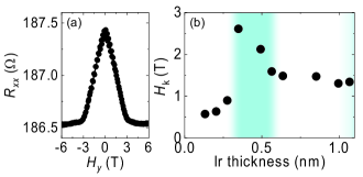
We use transport measurements to evaluate the anisotropy field of the multilayers. The longitudinal resistance of the Hall bar is measured as a function of in-plane magnetic field orthogonal to the current flow (along the axis). Typical plot of vs. from a multilayer with antiferromagnetic coupling is shown in Fig. 4(a). drops as is increased from zero due to the spin Hall magnetoresistance (SMR)Nakayama et al. (2013); Chen et al. (2013); Kim et al. (2016). The field at which saturates correspond to the the anisotropy field . The Ir layer thickness dependence of is plotted in Fig. 4(b). The results are similar to those reported in Ref. Lau et al. (2019). Note that the seed layer in this study is 3 Ta/2 Pt whereas it was 1 Ta/3 Ru in Ref. Lau et al. (2019).
References
- Manchon and Zhang (2009) A. Manchon and S. Zhang, Phys. Rev. B 79, 094422 (2009).
- Garello et al. (2018) K. Garello, F. Yasin, S. Couet, L. Souriau, J. Swerts, S. Rao, S. V. Beek, W. Kim, E. Liu, S. Kundu, D. Tsvetanova, K. Croes, N. Jossart, E. Grimaldi, M. Baumgartner, D. Crotti, A. Fumemont, P. Gambardella, and G. S. Kar, 2018 IEEE Symposium on VLSI Circuits , 81 (2018).
- Miron et al. (2011) I. M. Miron, K. Garello, G. Gaudin, P. J. Zermatten, M. V. Costache, S. Auffret, S. Bandiera, B. Rodmacq, A. Schuhl, and P. Gambardella, Nature 476, 189 (2011).
- Liu et al. (2012) L. Liu, C.-F. Pai, Y. Li, H. W. Tseng, D. C. Ralph, and R. A. Buhrman, Science 336, 555 (2012).
- Mellnik et al. (2014) A. R. Mellnik, J. S. Lee, A. Richardella, J. L. Grab, P. J. Mintun, M. H. Fischer, A. Vaezi, A. Manchon, E. A. Kim, N. Samarth, and D. C. Ralph, Nature 511, 449 (2014).
- Fan et al. (2014) Y. B. Fan, P. Upadhyaya, X. F. Kou, M. R. Lang, S. Takei, Z. X. Wang, J. S. Tang, L. He, L. T. Chang, M. Montazeri, G. Q. Yu, W. J. Jiang, T. X. Nie, R. N. Schwartz, Y. Tserkovnyak, and K. L. Wang, Nat. Mater. 13, 699 (2014).
- MacNeill et al. (2017) D. MacNeill, G. M. Stiehl, M. H. D. Guimaraes, R. A. Buhrman, J. Park, and D. C. Ralph, Nat. Phys. 13, 300 (2017).
- Zhang et al. (2014) W. Zhang, M. B. Jungfleisch, W. J. Jiang, J. E. Pearson, A. Hoffmann, F. Freimuth, and Y. Mokrousov, Phys. Rev. Lett. 113, 196602 (2014).
- Zhang et al. (2016) W. F. Zhang, W. Han, S. H. Yang, Y. Sun, Y. Zhang, B. H. Yan, and S. S. P. Parkin, Science Advances 2, e1600759 (2016).
- Fukami et al. (2016) S. Fukami, C. L. Zhang, S. DuttaGupta, A. Kurenkov, and H. Ohno, Nat. Mater. 15, 535 (2016).
- Chen et al. (2014) H. Chen, Q. Niu, and A. H. MacDonald, Phys. Rev. Lett. 112, 017205 (2014).
- Zhang et al. (2017) Y. Zhang, Y. Sun, H. Yang, J. Zelezny, S. P. P. Parkin, C. Felser, and B. H. Yan, Phys. Rev. B 95, 075128 (2017).
- Nakatsuji et al. (2015) S. Nakatsuji, N. Kiyohara, and T. Higo, Nature 527, 212 (2015).
- Nayak et al. (2016) A. K. Nayak, J. E. Fischer, Y. Sun, B. H. Yan, J. Karel, A. C. Komarek, C. Shekhar, N. Kumar, W. Schnelle, J. Kubler, C. Felser, and S. S. P. Parkin, Science Advances 2, e1501870 (2016).
- Duine et al. (2018) R. A. Duine, K. J. Lee, S. S. P. Parkin, and M. D. Stiles, Nat. Phys. 14, 217 (2018).
- Parkin et al. (1990) S. S. P. Parkin, N. More, and K. P. Roche, Phys. Rev. Lett. 64, 2304 (1990).
- Parkin et al. (1999) S. S. P. Parkin, K. P. Roche, M. G. Samant, P. M. Rice, R. B. Beyers, R. E. Scheuerlein, E. J. O’Sullivan, S. L. Brown, J. Bucchigano, D. W. Abraham, Y. Lu, M. Rooks, P. L. Trouilloud, R. A. Wanner, and W. J. Gallagher, J. Appl. Phys. 85, 5828 (1999).
- Roschewsky et al. (2016) N. Roschewsky, T. Matsumura, S. Cheema, F. Hellman, T. Kato, S. Iwata, and S. Salahuddin, Appl. Phys. Lett. 109, 112403 (2016).
- Finley and Liu (2016) J. Finley and L. Liu, Phys. Rev. Appl. 6, 054001 (2016).
- Mishra et al. (2017) R. Mishra, J. Yu, X. Qiu, M. Motapothula, T. Venkatesan, and H. Yang, Phys. Rev. Lett. 118, 167201 (2017).
- Ueda et al. (2017) K. Ueda, M. Mann, P. W. P. de Brouwer, D. Bono, and G. S. D. Beach, Phys. Rev. B 96, 064410 (2017).
- Zhang et al. (2018) P. X. Zhang, L. Y. Liao, G. Y. Shi, R. Q. Zhang, H. Q. Wu, Y. Y. Wang, F. Pan, and C. Song, Phys. Rev. B 97, 214403 (2018).
- Krishnia et al. (2019) S. Krishnia, C. Murapaka, P. Sethi, W. L. Gan, Q. Y. Wong, G. J. Lim, and W. S. Lew, J. Magn. Magn. Mater. 475, 327 (2019).
- Kim et al. (2017) K. J. Kim, S. K. Kim, Y. Hirata, S. H. Oh, T. Tono, D. H. Kim, T. Okuno, W. S. Ham, S. Kim, G. Go, Y. Tserkovnyak, A. Tsukamoto, T. Moriyama, K. J. Lee, and T. Ono, Nat. Mater. 16, 1187 (2017).
- Yang et al. (2015) S.-H. Yang, K.-S. Ryu, and S. Parkin, Nat. Nanotechnol. 10, 221 (2015).
- Caretta et al. (2018) L. Caretta, M. Mann, F. Buttner, K. Ueda, B. Pfau, C. M. Gunther, P. Hessing, A. Churikoval, C. Klose, M. Schneider, D. Engel, C. Marcus, D. Bono, K. Bagschik, S. Eisebitt, and G. S. D. Beach, Nat. Nanotechnol. 13, 1154 (2018).
- Kawaguchi et al. (2018) M. Kawaguchi, D. Towa, Y. C. Lau, S. Takahashi, and M. Hayashi, Appl. Phys. Lett. 112, 202405 (2018).
- Ishikuro et al. (2019) Y. Ishikuro, M. Kawaguchi, N. Kato, Y. C. Lau, and M. Hayashi, Phys. Rev. B 99, 134421 (2019).
- Pai et al. (2016) C.-F. Pai, M. Mann, A. J. Tan, and G. S. D. Beach, Phys. Rev. B 93, 144409 (2016).
- Knepper and Yang (2005) J. W. Knepper and F. Y. Yang, Phys. Rev. B 71, 224403 (2005).
- Lau et al. (2019) Y. C. Lau, Z. D. Chi, T. Taniguchi, M. Kawaguchi, G. Shibata, N. Kawamura, M. Suzuki, S. Fukami, A. Fujimori, H. Ohno, and M. Hayashi, Phys. Rev. Mater. 3, 104419 (2019).
- Amin et al. (2018) V. P. Amin, J. Zemen, and M. D. Stiles, Phys. Rev. Lett. 121, 136805 (2018).
- heon C. Baek et al. (2018) S. heon C. Baek, V. P. Amin, Y.-W. Oh, G. Go, S.-J. Lee, G.-H. Lee, K.-J. Kim, M. D. Stiles, B.-G. Park, and K.-J. Lee, Nat. Mater. 17, 509 (2018).
- Taniguchi et al. (2015) T. Taniguchi, J. Grollier, and M. D. Stiles, Phys. Rev. Appl. 3, 044001 (2015).
- Iihama et al. (2018) S. Iihama, T. Taniguchi, K. Yakushiji, A. Fukushima, Y. Shiota, S. Tsunegi, R. Hiramatsu, S. Yuasa, Y. Suzuki, and H. Kubota, Nature Electronics 1, 120 (2018).
- Amin et al. (2019) V. P. Amin, J. W. Li, M. D. Stiles, and P. M. Haney, Phys. Rev. B 99, 220405(R) (2019).
- Wang et al. (2019) W. Wang, T. Wang, V. P. Amin, Y. Wang, A. Radhakrishnan, A. Davidson, S. R. Allen, T. J. Silva, H. Ohldag, D. Balzar, B. L. Zink, P. M. Haney, J. Q. Xiao, D. G. Cahill, V. O. Lorenz, and X. Fan, Nat. Nanotechnol. 14, 819 (2019).
- Jamali et al. (2013) M. Jamali, K. Narayanapillai, X. P. Qiu, L. M. Loong, A. Manchon, and H. Yang, Phys. Rev. Lett. 111, 246602 (2013).
- Huang et al. (2015) K. F. Huang, D. S. Wang, H. H. Lin, and C. H. Lai, Appl. Phys. Lett. 107, 232407 (2015).
- Jinnai et al. (2017) B. Jinnai, C. L. Zhang, A. Kurenkov, M. Bersweiler, H. Sato, S. Fukami, and H. Ohno, Appl. Phys. Lett. 111, 102402 (2017).
- Yuasa et al. (2002) S. Yuasa, T. Nagahama, and Y. Suzuki, Science 297, 234 (2002).
- Stiles and Zangwill (2002) M. D. Stiles and A. Zangwill, Phys. Rev. B 66, 014407 (2002).
- Nakayama et al. (2013) H. Nakayama, M. Althammer, Y. T. Chen, K. Uchida, Y. Kajiwara, D. Kikuchi, T. Ohtani, S. Geprags, M. Opel, S. Takahashi, R. Gross, G. E. W. Bauer, S. T. B. Goennenwein, and E. Saitoh, Phys. Rev. Lett. 110, 206601 (2013).
- Chen et al. (2013) Y. T. Chen, S. Takahashi, H. Nakayama, M. Althammer, S. T. B. Goennenwein, E. Saitoh, and G. E. W. Bauer, Phys. Rev. B 87, 144411 (2013).
- Kim et al. (2016) J. Kim, P. Sheng, S. Takahashi, S. Mitani, and M. Hayashi, Phys. Rev. Lett. 116, 097201 (2016).