DFT-Based Engineering of Dirac Surface Energy
in Topological-Insulator Multilayers
Abstract
Aiming at the future spintronics device applications of the spin-polarized surface states in three-dimensional topological insulator, a highly insulating bulk state and a tunable Dirac cone surface state are required. Here we employ a slab model having hetero-structural Bi2Se3-related quintuple layers and perform first-principles simulations. Our computational results show that the Dirac-point energy can be optimally tuned by selecting an appropriate pair of materials so that the work function at the surface quintuple layer is slightly different from that at the inner quintuple layers. The ideal surface state is obtained in Bi2Te3/(Bi2Te2Se)4/Bi2Te3 slab, in which the Fermi lines show the significant warping effect and both the in-plane and the out-of-plane components of the spin polarization emerge.
1 Introduction
A three-dimensional topological insulator (TI) exhibits the non-trivial quantum states which can be characterized by the insulating bulk states and the spin-polarized metallic surface states[1, 2, 3, 4]. The latter is known to have the Dirac cone dispersion and show the spin polarized state, which has an appealing potential for future spintronics device applications. Although the highly insulating bulk state and the tunable Dirac cone in the bulk band gap are desired for the applications, many of topological insulators have been found to be metallic due to the existence of impurities and/or structural disorder. For example, in Bi2Se3, Se vacancies and Se anti-site defects lead to electron carrier doping in the conduction bands.[5, 6, 7, 8, 9] In Bi2Te3, Te (Bi) anti-site defects leads to electron (hole) carrier doping.[5][6][10] It has been also observed that the Dirac point is embedded in the bulk valence bands in Bi2Te3[11, 12, 13], which makes impossible to utilize the Dirac carrier. Recently, it has been reported that [14, 15] and solid solution[16, 17, 18] show highly bulk insulating states, because the defect formation can be suppressed by controlling the solid solution ratio in these materials. In these materials, the spin-polarized Dirac cones appear in the middle of the band gap, and therefore they are now considered as a good playground to experimentally investigate the topological surface bands. In the present study, by using first-principles calculations, we propose an alternative way to tune the Dirac-cone energy, that is, artificial stacking control of the Bi2Se3-related quintuple-layer slabs.
2 Method
2.1 Structural Models
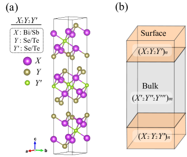
Three dimensional topological insulators, , , and , crystalize in ternary tetradymite structure as shown in Fig. 1 (a). The covalently bonded quintuple layers (QLs) are weakly stacked in the ABCABC sequence through van der Waals interaction. In this study, we set up a multi-QL periodic slab model which contains two kinds of topological-insulator materials selected out of , , , and (Note: among them, only is a trivial insulator). The multi-QL sequence is described as // ( = Bi or Sb, and = Te or Se) as shown in Fig. 1 (b). For the sake of simplicity, we consider only the centrosymmetric slab structure. We also validated that the six QL slab is thick enough to obtain the topologically protected surface bands.
2.2 Computational Details
Bandstructure calculations were performed by using a projector augmented wave method[19] implemented in Vienna Ab initio Simulation Package (VASP) code[20] with generalized gradient approximation (GGA)[21] to the density functional theory (DFT). To obtain accurate inter-QL distances, long-range van der Waals interaction was taken into account through semi-empirical corrections by DFT-D2 approach.[22] After the crystal structure was fully optimized until forces acting on atoms were smaller than eV/Å, the spin-orbit coupling was included self-consistently. The -point mesh was set to be . The in-plane experimental lattice parameter was used for the calculation; for Bi2Se3, Bi2Te2Se, Bi2Te3, Sb2Se3, and Sb2Te3, =4.143 [23], 4.280 [24], 4.382 [25], 4.034 [26], 4.250 [27] Å were used, respectively. For the hetero-structural slab calculation, the lattice parameter of the material located at the inner (bulk) part of slab was employed. The vacuum layer was set to be larger than 25 Å between the slabs.
3 Results
3.1 Homo-structural TI slabs
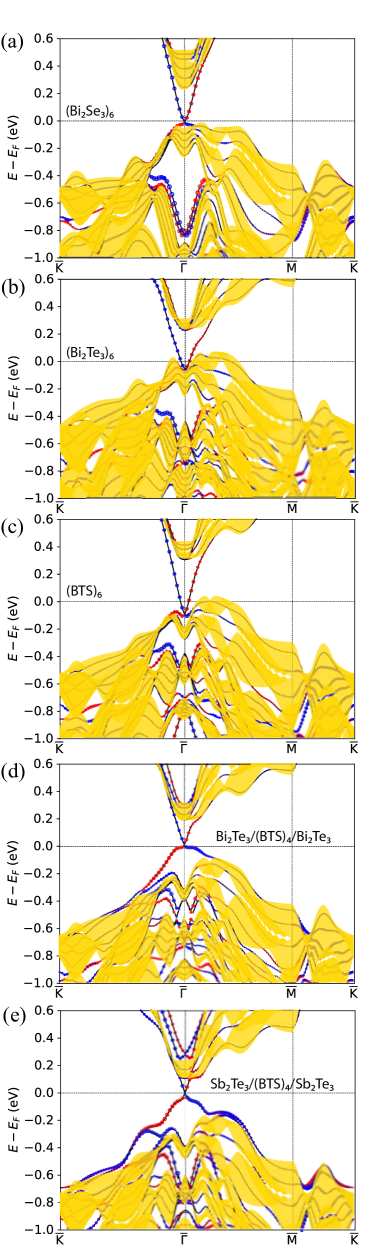
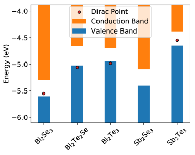
First we look at the calculated bandstructures of homo-structural slabs, i.e., (Bi2Se3)6, (Bi2Te3)6, and (Bi2Te2Se)6 slabs, as shown in Fig. 2 (a)-(c). The band gap of (Bi2Se3)6 is calculated as =0.31 eV, which is consistent with the experimentally measured band gap of bulk Bi2Se3, =0.2-0.3 eV.[28, 29] (Bi2Te3)6 shows smaller band gap, =0.27 eV. Among the three slabs, the band gap is largest, eV, at (Bi2Te2Se)6. In the slab calculation, the inner four QLs forms the bulk-like bands whereas an outmost QL forms the surface bands. The valence band maximum (VBM) of the bulk QL is found along the - path; the conduction band minimum (CBM) is found at the point. The spin-polarized Dirac-cone surface states appear at the point, while the Dirac point is located only 0.05 eV above the Fermi energy at (Bi2Se3)6 and the point is embedded into the valence bands at (Bi2Te2Se)6 and (Bi2Te3)6. These electronic structures are apparently not useful for the spintronics applications since the carriers are easily doped into the bulk valence bands and hard to exploit the Dirac carriers. Even worse, the spin current may leak out from the surface to the bulk due to the metallic bulk band structure. Therefore, it is needed to shift the Dirac point upward, away from the VBM to the middle of the energy gap. In order to achieve it, we adopt the following strategy: (1) set four QLs of Bi2Te2Se at the inner (bulk) slab to open the wide bulk band gap and (2) load the surface material which has shallower electron potential onto bulk (Bi2Te2Se)4 and make a hetero-structural junction so that the surface state energy is expected to be shifted upward. The computational results of the band-gap and the Dirac cone in the homo-structural TI slabs are summerized in Fig. 3. In the following section, we will present results of hetero-structural slabs as combining two types of TIs.
3.2 -based heterostructural TI slab
Following our strategy, several combinations of hetero-structural slabs by using Bi2Te2Se and other TIs were tested. Successful results were obtained only when Bi2Te3 or Sb2Te3 was chosen for the surface QL. As shown in Fig. 2 (d), the // hetero-structural slab shows the ideal TI surface-band structure, in which the Dirac point is located at the middle of the band gap at the point. As compared with the band structure of (Bi2Te2Se)6 (cfr. Fig. 2(c)), the bulk band gap is kept large as 0.32 eV, while the Dirac point is shifted upward in energy by 0.19 eV. The effect is simply caused by the replacement of outermost Se layer of the slab by Te layer.
In order to understand the shift of the surface-state energy, we evaluated the work function of slab structures. Table 1 (upper part) shows the work function of 6QL slabs that contain a single TI material, where the work function is defined as energy difference between bulk VBM and the potential at the vacuum region between slabs. That can be an indicator of the potential depth of each slab. It can be seen that the work function at (Bi2Te3)6, =4.95eV, is slightly shallower than that in (Bi2Te2Se)6, =5.02eV. The difference of these work functions, = +0.07 eV, is indeed responsible for the upward shift of the Dirac point in // multiQL; the surface bands arising from the outmost Bi2Te3 QL is shifted up relatively to the bulk bands arising from the inner (Bi2Te2Se)4 QLs. In the case of a multiQL //, as shown in Fig. 2 (e), the Dirac point is shifted further upward by 0.003 eV and approaches the bulk CBM. The trend is also depicted in Fig.4 (d). This can be understood by calculating the work function at (Sb2Te3)6, =4.65eV, that is smaller than those at (Bi2Te3)6 and (Bi2Te2Se)6.
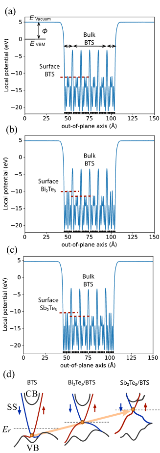
The energy difference caused between the surface QL and the inner QLs can be visualized by plotting the electron local potential. Figure 4 (a)-(c) shows the local potential along the out-of-plane axis in a super cell containing 6QL slab and the vacuum region. It is seen that the local potential is rather flat in Bi2Te2Se slab region and becomes shallower at a surface QL of Bi2Te3 and Sb2Te3.
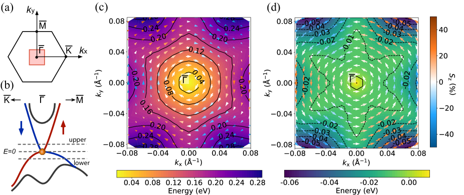
The Dirac surface state is characterized by intriguing properties such as spin-momentum locking caused by lack of space-inversion symmetry and presence of spin-orbit coupling. The isocontour of the surface-band energy and the spin texture of the Dirac surface states in // slab are shown in Fig. 5. It is noted that the constant-energy contour ofthe lower Dirac band shows strongly warped shape (that looks like a snowflake) while the upper Dirac band shows hexagonal-looking energy contour. The difference may come from the different characters of the bands; the upper Dirac band consists of mainly Bi orbital state and the lower consists of mainly Te state. The warping effect can be also seen in Bi2Te3 surface[30], while the effect is strongly enhanced in //, where the outmost Bi2Te3 surface QL is located between the vacuum region and Bi2Te2Se QLs and create the rather non-centrosymmetric electronic potential at the surface Bi atom. According to a perturbation theory [30] with spin-orbit coupling with -symmetry around the point, effective Hamiltonian up to the third order of reads
| (1) |
Here, the first term is free-electron dispersion with the mass . The second term with the Dirac velocity and the in-plane spin momentum is responsible for two-dimensional Rashba effect. The last term is essential for the Fermi-line warping (here ) and also emergence of the out-of-plane spin polarization . In fact, as shown in Fig. 5 (c), the spin texture of the lower Dirac band shows not only the Rashba-type tangential spin vortex but also the out-of-plane spin component along the line away from the point.[31] The upper and lower bands basically show the opposite directions of spin polarization.
| Slab | |||
| (eV) | (eV) | (eV) | |
| 0.305 | 5.603 | +0.052 | |
| 0.251 | 4.946 | -0.121 | |
| 0.366 | 5.024 | -0.091 | |
| 0.314 | 5.404 | None | |
| 0.267 | 4.650 | +0.101 | |
| // | 0.269 | 5.471 | +0.016 |
| // | Metal | ||
| // | Metal | ||
| // | 0.199 | 4.940 | +0.035 |
| // | 0.237 | 4.949 | +0.006 |
| // | 0.165 | 4.891 | -0.031 |
| // | Metal | ||
| // | Metal | ||
| // | Metal | ||
| // | 0.321 | 4.947 | +0.096 |
| // | 0.290 | 4.923 | +0.113 |
| // | 0.253 | 4.853 | +0.051 |
| // | 0.221 | 4.817 | +0.029 |
| // | 0.172 | 4.825 | +0.038 |
| // | 0.160 | 4.782 | -0.023 |
| // | 0.143 | 4.806 | -0.023 |
| // | Metal | ||
| // | 0.265 | 4.836 | +0.158 |
| // | 0.263 | 4.830 | +0.146 |
| // | 0.225 | 4.761 | +0.150 |
| // | 0.189 | 4.724 | +0.127 |
| // | 0.229 | 4.664 | +0.089 |
| // | 0.136 | 4.651 | +0.050 |
| // | 0.207 | 4.569 | -0.005 |
| // | 0.271 | 4.685 | +0.007 |
In order to find the optimal Dirac surface state, more than 20 types of hetero-structural topological QL slabs were examined. The calculated results of the energy gap and the Dirac-point energy are summarized in Table 1. Among these heterostructure candidates, the ideal Dirac surface state which form the crossing point at the middle of the wide band gap is found at //, //, //, //, and //. In these slabs, as discussed above, the bulk Bi2Te2Se QLs opens the wide band gap ( eV) and the surface Dirac cone originating from Bi2Te3 and Sb2Te3 QLs appears at the middle of the gap; the shallower work function of the surface QL with respect to that of the bulk QL slightly shifts up the surface state energy; e.g., slab shows eV and shows eV. As varying the number of Sb2Te3 and Bi2Te2Se QLs at // slabs, it is feasible to tune the position of the Dirac cone in the wide energy region (). On the other hand, when we combine two types of QL-materials whose work functions are much different, the hetero-structural slab goes metallic. For example, the Bi2Se3 and Bi2Te3 6QL slabs show 5.60 and 4.95 eV, respectively, and then the hetero-structural combination of these QLs is found to be metallic. In // slabs, it is metallic not only at the surface state but also at the bulk state because the CBM of Bi2Se3 overlaps with the VBM of Bi2Te3 (see Fig. 3).
4 Summary
First-principles DFT calculations have been carried out on the hetero-structural multi-QL slabs of topological insulators. We have demonstrated that the Dirac-point position can be shifted to the middle of the band gap by combining the appropriate pair of QLs of different materials. The surface-band energy can be further tuned by varying the number of QLs in the slab. Since the controllability of Dirac cone can be acquired by simple combination of the conventional topological insulators, it may be easily confirmed by following experimental studies and promising for future spintronics applications.
KY acknowledges Takafumi Sato and Seigo Souma for the fruitful discussions on topological materials. This work was supported by JSPS Kakenhi (No. 17H02916 and 18H04227) and by JST-CREST (No: JPMJCR18T1). A part of the computation in this work has been done by using the facilities of the Supercomputer Center, the Institute for Solid State Physics, the University of Tokyo. The crystallographic figure was generated using VESTA program.[32]
References
- [1] M. Z. Hasan and C. L. Kane, Rev. Mod. Phys. , 3045 (2010) .
- [2] X.-L. Qi and S.-C. Zhang, Rev. Mod. Phys. , 1057 (2011).
- [3] Y. Xia, D. Qian, D. Hsieh, L. Wray, A. Pal, H. Lin, A. Bansil, D. Grauer, Y. S. Hor, R. J. Cava and M. Z. Hasan, Nature Phys. , 398 (2009).
- [4] J. E. Moore, Nature (London) , 194 (2010).
- [5] D. O. Scanlon, P. D. C. King, R. P. Singh, A. de la Torre, S. M. Walker, G. Balakrishnan, F. Baumberger, and C. R. A. Catlow, Adv. Mater. , 2154 (2012) .
- [6] L.-L. Wang, M. Huang, S. Thimmaiah, A. Alam, S. L. Bud’ko, A. Kaminski, T. A. Lograsso, P. Canfield, and D. D. Johnson, Phys. Rev. B , 125303 (2013) .
- [7] N. P. Butch, K. Kirshenbaum, P. Syers, A. B. Sushkov, G. S. Jenkins, H. D. Drew, and J. Paglione, Phys. Rev. B , 241301 (2010).
- [8] J. G. Analytis, J.-H. Chu, Y. Chen, F. Corredor, R. D. McDonald, Z. X. Shen, and I. R. Fisher, Phys. Rev. B , 205407 (2010).
- [9] K. Eto, Z. Ren, A. A. Taskin, K. Segawa, and Y. Ando, Phys. Rev. B , 195309 (2010) .
- [10] D.-X. Qu, Y. S. Hor, J. Xiong, R. J. Cava, and N. P. Ong, Science , 821 (2010).
- [11] Y. Xia, D. Qian, D. Hsieh, L. Wray, A. Pal, H. Lin, A. Bansil, D. Grauer, Y. S. Hor, R. J. Cava, and M. Z. Hasan, Nat. Phys. 5, 398 (2009).
- [12] Y. L. Chen, J. G. Analytis, J.-H. Chu, Z. K. Liu, S.-K. Mo, X. L. Qi, H. J. Zhang, D. H. Lu, X. Dai, Z. Fang, S. C. Zhang, I. R. Fisher, Z. Hussain, and Z.-X. Shen, Science , 178 (2009).
- [13] D. Hsieh, Y. Xia, D. Qian, L. Wray, F. Meier, J. H. Dil, J. Osterwalder, L. Patthey, A. V. Fedorov, H. Lin, A. Bansil, D. Grauer, Y. S. Hor, R. J. Cava, and M. Z. Hasan, Phys. Rev. Lett. , 146401 (2009).
- [14] Z. Ren, A. A. Taskin, S. Sasaki, K. Segawa, and Y. Ando, Phys. Rev. B , 155301 (2012).
- [15] J. Xiong, A. C. Petersen, D. Qu, Y. S. Hor, R. J. Cava, and N. P. Ong, Physica E , 917 (2012).
- [16] Z. Ren, A. A. Taskin, S. Sasaki, K. Segawa, and Y. Ando, Phys. Rev. B , 241306(R) (2010).
- [17] T. Arakane, T. Sato, S. Souma, K. Kosaka, K. Nakayama, M. Komatsu, T. Takahashi, Z. Ren, K. Segawa, and Y. Ando, Nature Commun. , 636 (2012).
- [18] A. A. Taskin, Z. Ren, S. Sasaki, K. Segawa, and Y. Ando, Phys. Rev. Lett. , 016801 (2011).
- [19] P. E. Blöchl, Phys. Rev. B , 17953 (1994).
- [20] G. Kresse, J. Furthmüller, Phys. Rev. B , 11169 (1996).
- [21] J. P. Perdew, K. Burke and M. Ernzerhof, Phys. Rev. Lett. , 3865 (1996).
- [22] S. Grimme, J. Comput. Chem. , 1787 (2006) .
- [23] S. Nakajima, J. Phys. Chem. Solids , 479 (1963).
- [24] J. A. Bland and S. J. Basinski, Can. J. Phys. , 1040 (1961).
- [25] Y. Miyazaki and T. Kajitani, J. of Crys. Growth, , 542 (2001).
- [26] Since the experimental lattice constants for Sb2Se3 were not found in literatures, the lattice structure was obtained by lattice optimization.
- [27] R. W. G. Wyckoff, Crystal Structures 2 (Wiley, New York, 1964); Th. L. Anderson, H. Krause and H. Brigitte, Acta Crystallogr. B , 1307 (1974).
- [28] I. A. Nechaev et al., Phys. Rev. B 87, 121111 (2013).
- [29] G. Martinez et al., Sci Rep. 7, 6891 (2017).
- [30] L. Fu, Phys. Rev. Lett. , 266801 (2009).
- [31] S. Souma, K. Kosaka, T. Sato, M. Komatsu, A. Takayama, T. Takahashi, M. Kriener, K. Segawa, and Y. Ando, Phys. Rev. Lett. , 216803 (2011).
- [32] K. Momma and F. Izumi, J. Appl. Crystallogr. , 1272 (2011).