Demonstration of focal length tuning by rotational varifocal moiré metalens in an ir-A wavelength
††journal: oehttps://nmems.lab.tuat.ac.jp/en/
This paper reports an experimental demonstration of moiré metalens which shows wide focal length tunability from negative to positive by mutual angle rotation at the wavelength of 900 nm. The moiré metalens was developed using high index contrast transmitarray meta-atoms made of amorphous silicon octagonal pillars, which is designed to have polarization insensitivity and full 2 phase coverage. The fabricated moiré metalens showed focal length tunability at the ranges between 1.73 – 5 mm, which corresponds to the optical power ranges between 578 – 200 m-1 at the mutual rotation between degrees.
1 Introduction
Metasurfaces, a planar branch of metamaterials, have attracted significant attention because of its possibility to tailor optical wavefront by arranging subwavelength patterns (meta-atoms) on the surface.[1, 2, 3] They are able to show unique optical properties that cannot be achieved in natural materials and have a high affinity for micro/nanofabrication methods including lithography, deposition, and etching. Therefore, metasurfaces have opened up many research fields and applications including lens[4, 5, 6, 7], retarders and waveplates[8, 9, 10, 11], vector beam converters[12, 13, 14], color filters[15, 16, 17], holography[18, 19, 20, 21, 22], zero refractive index materials[23], and others. It should be emphasized that mechanical deformation or change of mutual geometric position of metasurfaces offers novel functionality and tunability for their optical properties. Based on this idea, reconfigurable metasurfaces have been studied including tunable transmittance[24], color tuning[25], active phase shifters[26, 27], and so on.
Metasurface lens, or metalens, has been attracted many interests because of its thinness and lightweight. Especially, recent developments of lossless dielectric metalenses[28, 5, 6] have been boosted attention to this field. The integration of the metalens with microelectromechanical systems (MEMS) enables both compactness and functionalities[29]. Tunable focal length, or varifocal lens, is one of the most promising and expected functionalities of metalens. Similar to conventional refractive lens doublet, the longitudinal motion of lenses along with the optical axis based on a MEMS actuator has been demonstrated[30]. However, the pull-in instability effect of electrostatic parallel plates actuator limits the travel range of metalens[31, 32] and resulting in a narrow tunable range of focal length.
As metalens has much design freedom, a tuning method of the focal length is not necessary to be similar to conventional refractive lenses. Actually, studying diffractive optical elements (DOEs) or diffractive lenses may bring many advantages to metalens. In fact, DOEs-inspired tunable metalens, Alvarez metalens, has been experimentally demonstrated, and focal length tuning based on lateral movement of a pair of lenses was achieved[33, 34, 35]. Furthermore, the integration with the MEMS actuator to the Alvarez lens dynamic focal length control with the compact actuation mechanism[36]. However, the experimental tuning range of the focal length was limited to the positive region, in contrast to the potential capability to both positive and negative of the Alvarez configuration. Furthermore, the lateral motion of the Alvarez lens limits the effective area (the aperture) of the lens.
Moiré lens is a doublet of axially-asymmetric lenses that show tunable focal length with mutual rotation as shown in Figure 1(a)[37, 38]. It can offer a wide range of focal lengths from negative to positive and has been realized using diffractive optical elements (DOEs)[39, 40]. Moiré metalens has also been studied with numerical simulations[41, 42], and quite recently experimentally demonstrated in microwave frequency[43] and the infrared-B (ir-B) wavelength[44]. However, the continuous promotion of shorter wavelengths and larger diameters are required increasingly on metalenses, despite the manufacturing difficulty[45, 46], especially in the axially-asymmetric lenses.
Here, we experimentally demonstrate tunable focal length with moiré metalens at the ir-A wavelength of 900 nm using polarization-insensitive meta-atom based on high index contrast transmitarrays (HCTAs), specifically made of amorphous silicon (a-Si) in this case. A-Si octagonal pillars were designed to have polarization insensitivity and full 2 phase coverage at the wavelength of 900 nm in order to use a character projection (CP) type electron beam lithography (EBL) apparatus for high-throughput drawing. The metalens is designed to satisfy the phase distribution of moiré metalens as detailed below by mapping corresponding pillars to each lattice point with a hexagonal basis. The designed metalens was successfully fabricated with a diameter of 2 mm, which is the largest among EBL-drawn varifocal metalenses on a glass substrate using simple a-Si sputter deposition, EBL using CP, metal mask lift-off, and reactive ion etching (RIE) of silicon. The fabricated metalens showed focal length tunability at the ranges between 1.73 – 5 mm at the mutual rotation between degrees at the wavelength of 900 nm. The results reported here demonstrate a proof of concept for the focal length tuning with a mutual rotation of lens components based on moiré lens configuration at the wavelength, and pave the way to applications in optical frequencies including near-infrared, visible, and ultraviolet wavelengths.
2 Design and fabrication of moiré metalens
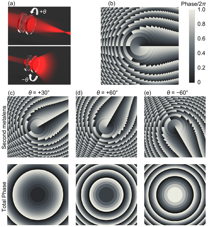
Figure1 shows a schematic drawing of moiré metalens. As shown in Fig. 1(a), moiré metalens consists of two metalenses, and their total focal length can be tuned by mutual rotation from negative to positive. Each part of a moiré metalens pair were designed to have transmission function distributions in polar coordinates [37],
| (1) |
where is a constant. The phase distribution of the first lens is shown in Fig. 1(b). With mutual rotation , the joint transmission function can be given by
| (2) |
This equation is similar to that of a spherical lens under paraxial approximation , where is the focal length and is the wavelength. So, by adjusting the constant to satisfy the equation , the optical power becomes proportional to the mutual rotation angle . Note that the round function is used to avoid the sectoring effect[37].
Figures 1(c-e) show phase distributions of the second metalens with mutual rotation angles of +30, +60, and –60 degrees, respectively, together with total phase distributions superimposed with the first metalens, shown in Fig. 1(b). As shown in Figs. 1(c) and (d), positive rotation angles create total phase distribution similar to convex Fresnel lens, and a larger rotation angle makes a higher phase gradient, which corresponds to short focal length and higher optical power. In contrast, as shown in Fig. 1(e), a negative rotation angle creates concave-like phase distribution. As shown here, by adopting moiré metalens, a wide tuning range of focal length from negative to positive can be expected.
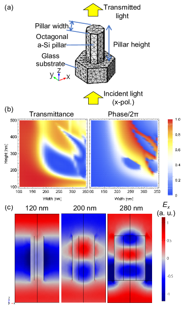
An a-Si octagonal pillar HCTAs have been adopted as polarization insensitive meta-atoms[28]. An octagonal shape was chosen in order to use CP of the EBL apparatus for the high-throughput fabrication as detailed later. An electromagnetic simulation was performed using a commercially available finite element method software COMSOL Multiphysics ver. 5.1 (COMSOL Inc., USA) as shown in Fig. 2. Figure 2(a) shows a schematic of the simulation setup. An octagonal pillar was situated on the silica glass substrate with a period of 400 nm. The surrounding medium of the pillar is air (not shown). The -polarized light at the wavelength of 900 nm incidents from the glass bottom side, then transmittance and phase delay of the pillar was evaluated at the output port (the air side). Froquet periodic boundary conditions are applied to boundaries parallel to -axis. An a-Si material parameter was used to the Si pillar[47].
Fig. 2(b) shows the parameters sweep results of transmittance and phase/2, by changing both pillar width and height with 10 nm steps. As a result, it was found that the region around height nm is able to achieve both high transmittance and full 2 phase coverage. Fig. 2(c) shows the component of electric field distribution at the pillar height of 400 nm and widths of 120, 200, 280 nm, respectively. It is clearly shown that phase difference between 200, 280 nm pillars, and 120 nm pillar at the output port (Top of the image) are corresponding to , and , respectively. Therefore, considering the fabrication process limitation for high aspect ratio structure, we adopted 400-nm-height pillars as the meta-atom.
Using these octagonal pillars as meta-atoms, moiré metalens with a diameter of 2 mm was designed. The "a" parameter was set to 0.001283 rad-1µm-2 to have maximum optical powers of at the mutual rotation angles degrees. It corresponds to the maximum numerical aperture (NA) of the moiré metalens to be 0.5. A GDSII CAD file of the moiré metalens was prepared by mapping pillars with corresponding phase delay satisfying the phase distribution described by of the equation 1 to each lattice point with a hexagonal basis with the pitch of 400 nm using a Python library gdspy[48].
A metalens was fabricated on a quartz glass substrate. The detailed fabrication process is available in Supplement 1 Section S1. An amorphous silicon film with a thickness of 400 nm was sputter-deposited. The optical properties of the deposited silicon thin film are shown in Supplement 1 Section S2. A lens pattern with a diameter of 2 mm was drawn by electron beam lithography with octagonal CP (Advantest F7000-S, Advantest, Japan) using dedicated octagonal stencil masks in order to achieve high drawing throughput. The GDSII CAD file described above was converted into CP shot data with proximity effect compensation (PEC). Octagonal CPs with the nominal width-across-flats from 120 to 280 nm with a step of 10 nm were used. Thanks to the high-throughput of CPs, a 2-cm-diameter moiré metalens, which consists of approximately meta-atoms with the GDSII file size of 1.2 GB, can be drawn less than 5 minutes exposure. After the resist development, an aluminum mask was patterned on the a-Si film through the lift-off process. Si pillars are formed by reactive ion etching. Finally, the aluminum mask was removed by a wet chemical.
3 Results and discussion
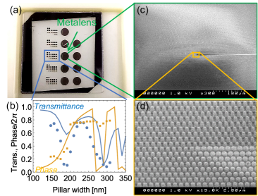
Figure 3 shows a photograph of fabricated lenses on a 2-cm-square glass substrate (a), transmission properties (b), and scanning electron microscope (SEM) images (c-d). In Fig. 3(a) Nine circles are 2-mm-diameter metalenses. Blue-indicated square patterns are pillar arrays with constant widths for transmission property measurements. Fig. 3(b) shows the transmission properties of the pillars as a function of pillar width at the wavelength of 900 nm. Dots indicate measurement results, and lines indicate COMSOL simulation. Blue and orange correspond to transmittance and phase/2, respectively. Data points in Fig. 3(b) is based on measured widths of pillars as detailed in the Supplement 1 Section S3. The phase delays of the pillars were measured by the interference method[49], using a laser diode and microspectroscopy system (Techno-Synergy, DF-1037) detailed in the Supplement 1 Section S4. Fig. 3(c) shows the SEM image of the lens, and 3(d) shows its close-up to the center, observed with 45∘ tilting angles. Width-distributed pillars are successfully fabricated. Because of fabrication limitation, pillars become not octagonal but cylindrical.
As shown in Fig. 3(b), as the width increases, phase delay rapidly increases on both simulation and experiment. Although the experimental transmittance becomes smaller than that of simulation, the position of dips is similar. The difference between experiment and simulation is considered to be attributed to fabrication error, including the rounded shape of the pillar top as shown in 3(d).
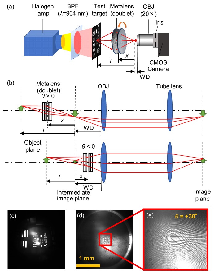
Figure 4 shows the experimental setup for focal length measurement. The optical system is shown in Fig. 4(a). A tungsten halogen white light source was used. And then the incident light passes through a band pass filter (#65-184, Edmund Optics USA, OD = 4, center wavelength = 904 nm, FWHM = 10 nm) and a test target (USAF 1951). A moiré metalens sample is prepared by assembling two metalens pieces fabricated through the above-mentioned process. The latter lens was flipped upside down along with the horizontal axis, to satisfy the phase distribution of in the equation 1. These lenses are aligned carefully under the microscope observation and adhered to using a tape with certain mutual rotation angles . The transmitted image of the USAF target was captured using a CMOS camera (DCC1545M, Thorlab Co., USA) with a 20X objective lens and an iris. The metalens and the USAF target were mounted on micrometer stages, respectively, and their position and were measured with 0.1 mm step.
Fig. 4(b) shows a detailed ray illustration for both positive (upper) and negative (lower) rotation angles.
Fig. 4(c) shows a captured image without moiré metalens and focused on the test target. The bright part which is due to the light source can be seen in the center. Figs. 4(d) shows the image focused onto the moiré metalens doublet. The lens diameter of 2 mm was almost equivalent to the iris opening. And Fig. 4(e) shows the magnified image of (d). The mutual rotation angle of 30 deg. are clearly seen. The lateral misalignment between two lenses was less than 4 µm, which corresponds to 10 pixels of meta-atom. It is considered that this misalignment does not much affect the focal length and efficiency, compared with literature on diffractive moiré lenses[37, 39].
Using the metalens position from the image plane and target position as shown in 4(a) under the certain mutual rotation angle , the focal length of the moiré metalens was calculated using the following equation,
| (3) |
Determination procedure of the focal length was summarized in Fig. 5. Fig. 5(a) shows a captured image of the group 4, number 2 of the USAF target obtained with the rotation angle and the lens position mm. The normalized gray level profile along the yellow line is shown in Fig. 5(b). In this profile, the resolution was defined as the average of the widths between the gray values of 0.1 and 0.9 with the linear interpolation between the data points. Fig. 5(c) summarizes the resolution as the function of the lens position . In this case, the focal position was determined to mm, which corresponds to the focal length mm.
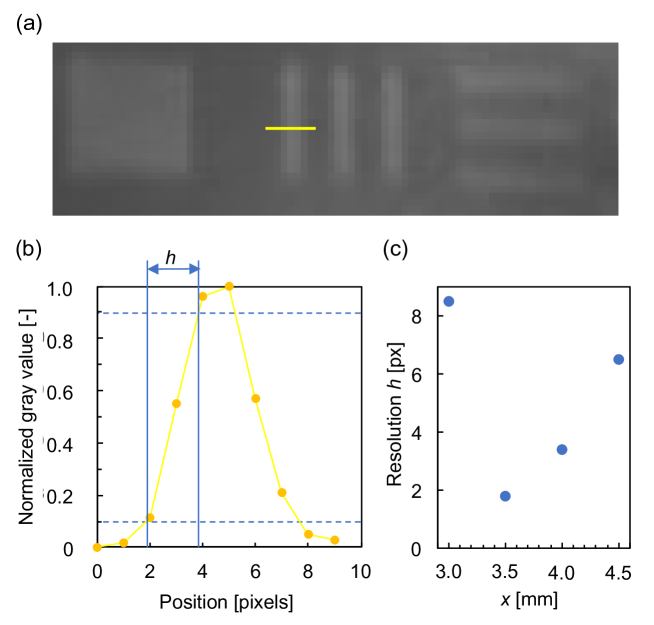
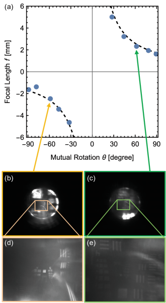
Figure 6 shows the measurement results of focal length (a) and typical imaging results (b-e). In Fig. 6(a), circle markers show experimental results obtained from the setup shown in Fig. 4. The dashed curve shows designed characteristics . Note that all standard deviations of the data points are smaller than the diameter of each marker. The experimental results agree very well with the design, and focal length tuning from negative to positive has been demonstrated at the wavelength of 900 nm. (b) and (c) show captured images at the nominal rotation angles of –60 and +60 degrees, respectively. (d) and (e) show magnified images of (b) and (c). Note that inverted real images are shown in (c) and (e), which corresponds to a positive focal length. In contrast, straight virtual images are shown in (b) and (d), which corresponds to negative focal length. However, for both negative and positive rotation angles, the contrast of the obtained images was not so high. A possible reason for this is considered as the stray light as shown in fig. 4(c).
The obtained result of this research was summarized in Table 1 in comparison with other papers related to mechanically tunable varifocal metalenses. As shown in this table, results from this paper show a wide tunable range of both the focal length and the optical power from both negative to positive. In short, metalens can be tuned as both convex and concave lenses. Furthermore, this lens achieved the largest size of 2 mm in diameter among EB-drawn metalenses ([30, 33, 36, 44]) due to the high throughput of CP exposure.
| Reference | Method | Focal Length [mm] | Optical Power [m] | Wavelength [nm] | Size [mm] |
|---|---|---|---|---|---|
| Arbabi et al. [30] | Lateral, MEMS | 0.565 – 0.629 | 1590 – 1770 | 915 | 0.5 |
| Zhang et al. [33] | Alvarez | 0.5 – 3 | 333 – 2000 | 633 | 0.15 |
| Colburn et al. [34] | Alvarez | 34 – 99 | 10 – 29 | 1550 | 10 |
| Colburn et al. [34] | Alvarez | 86 – 303 | 3 – 12 | 633 | 10 |
| Han et al. [36] | Alvarez, MEMS | +0.18 – +0.25 | +4000 – +5460 | 1550 | 0.5 |
| Wei et al. [44] | Moiré | 3 – 54 | 19 – 333 | 1550 | 1 |
| This work | Moiré | 1.73 – 5 | 200 –578 | 900 | 2 |
Although alignment and adhesion processes were used in this paper, as MEMS-actuated rotational stages have been reported, micro-rotational varifocal metalens will be realized by proper integration with actuators. And, in this case, we have tried a 2-mm-diameter lens, it would be possible to extend it to cm-scale in principle, because of the high throughput advantage of CP-based EB lithography.
4 Conclusion
In conclusion, focal length tuning by a rotational varifocal metalens, or moiré metalens, has been demonstrated in this paper at the ir-A wavelength of 900 nm. The metalens was designed using polarization-insensitive a-Si HCTAs as meta-atoms. The largest diameter of 2 mm among EBL-drawn varifocal metalenses was achieved because of the help of CP-based EB lithography apparatus with high drawing throughput. The fabricated metalens has shown focal length tuning at the ranges of 1.73 – 5 mm at the mutual rotation between degrees, which corresponding to the optical power tuning range of 200 – 578 m-1.
Funding
This work was supported by the Japan Society for the Promotion of Science (JSPS) grant-in-aid Nos. 17H02754, 19H02103, and 19H02607.
Acknowledgments
This research was supported by the Nanotechnology Platform site at the University of Tokyo, which is supported by the Ministry of Education, Culture, Sports, Science, and Technology (MEXT), Japan. The authors thank Prof. Yoshio Mita, and Dr. Eric Lebrasseur for their help with electron beam lithography and reactive ion etching, Prof. Kuniaki Konishi for his help with ellipsometry, and Prof. Lucas H. Gabrielli for the development of gdspy.
Disclosures
The authors declare no conflicts of interest.
See Supplement 1 for supporting content.
References
- [1] N. I. Zheludev and Y. S. Kivshar, “From metamaterials to metadevices,” \JournalTitleNature Materials 11, 917–924 (2012).
- [2] S. B. Glybovski, S. A. Tretyakov, P. A. Belov, Y. S. Kivshar, and C. R. Simovski, “Metasurfaces: From microwaves to visible,” \JournalTitlePhysics Reports 634, 1–72 (2016).
- [3] N. Yu and F. Capasso, “Flat optics with designer metasurfaces,” \JournalTitleNature Materials 13, 139–150 (2014).
- [4] X. Ni, S. Ishii, A. V. Kildishev, and V. M. Shalaev, “Ultra-thin, planar, Babinet-inverted plasmonic metalenses,” \JournalTitleLight: Science & Applications 2, e72 (2013).
- [5] M. Khorasaninejad, W. T. Chen, R. C. Devlin, J. Oh, A. Y. Zhu, and F. Capasso, “Metalenses at visible wavelengths: Diffraction-limited focusing and subwavelength resolution imaging,” \JournalTitleScience 352, 1190–1194 (2016).
- [6] S. Wang, P. C. Wu, V. C. Su, Y. C. Lai, M. K. Chen, H. Y. Kuo, B. H. Chen, Y. H. Chen, T. T. Huang, J. H. Wang, R. M. Lin, C. H. Kuan, T. Li, Z. Wang, S. Zhu, and D. P. Tsai, “A broadband achromatic metalens in the visible,” \JournalTitleNature Nanotechnology 13, 227–232 (2018).
- [7] T. Suzuki, K. Endo, and S. Kondoh, “Terahertz metasurface ultra-thin collimator for power enhancement,” \JournalTitleOptics Express 28, 22165–22178 (2020).
- [8] M. A. Kats, P. Genevet, G. Aoust, N. Yu, R. Blanchard, F. Aieta, Z. Gaburro, and F. Capasso, “Giant birefringence in optical antenna arrays with widely tailorable optical anisotropy,” \JournalTitleProceedings of the National Academy of Sciences of the United States of America 109, 12364–12368 (2012).
- [9] N. Yu, F. Aieta, P. Genevet, M. A. Kats, Z. Gaburro, and F. Capasso, “A Broadband, Background-Free Quarter-Wave Plate Based on Plasmonic Metasurfaces,” \JournalTitleNano Letters 12, 6328–6333 (2012).
- [10] M. Ishii, K. Iwami, and N. Umeda, “An Au nanofin array for high efficiency plasmonic optical retarders at visible wavelengths,” \JournalTitleApplied Physics Letters 106, 021115 (2015).
- [11] M. Ishii, K. Iwami, and N. Umeda, “Highly-efficient and angle-independent zero-order half waveplate at broad visible wavelength based on Au nanofin array embedded in dielectric,” \JournalTitleOptics Express 24, 7966–7976 (2016).
- [12] P. Genevet, N. Yu, F. Aieta, J. Lin, M. A. Kats, R. Blanchard, M. O. Scully, Z. Gaburro, and F. Capasso, “Ultra-thin plasmonic optical vortex plate based on phase discontinuities,” \JournalTitleApplied Physics Letters 100, 013101 (2012).
- [13] K. Iwami, M. Ishii, Y. Kuramochi, K. Ida, and N. Umeda, “Ultrasmall radial polarizer array based on patterned plasmonic nanoslits,” \JournalTitleApplied Physics Letters 101, 161119 (2012).
- [14] D. Hakobyan, H. Magallanes, G. Seniutinas, S. Juodkazis, and E. Brasselet, “Tailoring Orbital Angular Momentum of Light in the Visible Domain with Metallic Metasurfaces,” \JournalTitleAdvanced Optical Materials 4, 306–312 (2016).
- [15] N. Ikeda, Y. Sugimoto, M. Ochiai, D. Tsuya, Y. Koide, D. Inoue, A. Miura, T. Nomura, H. Fujikawa, and K. Sato, “Color Filter Based on Surface Plasmon Resonance Utilizing Sub-Micron Periodic Hole Array in Aluminum Thin Film,” \JournalTitleIEICE Transactions on Electronics E95-C, 251–254 (2012).
- [16] Y. Nagasaki, M. Suzuki, I. Hotta, and J. Takahara, “Control of Si-Based All-Dielectric Printing Color through Oxidation,” \JournalTitleACS Photonics 5, 1460–1466 (2018).
- [17] Y. Nagasaki, I. Hotta, M. Suzuki, and J. Takahara, “Metal-Masked Mie-Resonant Full-Color Printing for Achieving Free-Space Resolution Limit,” \JournalTitleACS Photonics 5, 3849–3855 (2018).
- [18] L. Huang, X. Chen, H. Mühlenbernd, H. Zhang, S. Chen, B. Bai, Q. Tan, G. Jin, K.-W. Cheah, C.-W. Qiu, J. Li, T. Zentgraf, and S. Zhang, “Three-dimensional optical holography using a plasmonic metasurface.” \JournalTitleNature communications 4, 2808 (2013).
- [19] Y. Yifat, M. Eitan, Z. Iluz, Y. Hanein, A. Boag, and J. Scheuer, “Highly Efficient and Broadband Wide-Angle Holography Using Patch-Dipole Nanoantenna Reflectarrays,” \JournalTitleNano Letters 14, 2485–2490 (2014).
- [20] Y.-W. Huang, W. T. Chen, W.-Y. Tsai, P. C. Wu, C.-M. Wang, G. Sun, and D. P. Tsai, “Aluminum Plasmonic Multicolor Meta-Hologram,” \JournalTitleNano Letters 15, 3122–3127 (2015).
- [21] W. Wan, J. Gao, and X. Yang, “Full-Color Plasmonic Metasurface Holograms,” \JournalTitleACS Nano 10, 10671–10680 (2016).
- [22] R. Izumi, S. Ikezawa, and K. Iwami, “Metasurface holographic movie: a cinematographic approach,” \JournalTitleOptics Express 28, 23761–23770 (2020).
- [23] T. Suzuki and H. Asada, “Reflectionless zero refractive index metasurface in the terahertz waveband,” \JournalTitleOptics Express 28, 21509–21521 (2020).
- [24] J. Y. Ou, E. Plum, L. Jiang, and N. I. Zheludev, “Reconfigurable Photonic Metamaterials,” \JournalTitleNano Letters 11, 2142–2144 (2011).
- [25] H. Honma, K. Takahashi, M. Ishida, and K. Sawada, “A Low-Voltage and High Uniformity Nano-Electro-Mechanical System Tunable Color Filter Based on Subwavelength Grating,” \JournalTitleJapanese Journal of Applied Physics 51, 11PA01 (2012).
- [26] K. Yamaguchi, H. Yamanaka, T. Ohtsu, and S. Ishii, “Electrically driven plasmon chip: Active plasmon lens in the visible range,” \JournalTitleApplied Physics Letters 108, 111903 (2016).
- [27] T. Shimura, T. Kinoshita, Y. Koto, N. Umeda, and K. Iwami, “Birefringent reconfigurable metasurface at visible wavelengths by MEMS nanograting,” \JournalTitleApplied Physics Letters 113, 171905 (2018).
- [28] A. Arbabi, Y. Horie, A. J. Ball, M. Bagheri, and A. Faraon, “Subwavelength-thick lenses with high numerical apertures and large efficiency based on high-contrast transmitarrays,” \JournalTitleNature Communications 6, 7069 (2015).
- [29] T. Roy, S. Zhang, I. W. Jung, M. Troccoli, F. Capasso, and D. Lopez, “Dynamic metasurface lens based on MEMS technology,” \JournalTitleAPL Photonics 3, 021302 (2018).
- [30] E. Arbabi, A. Arbabi, S. M. Kamali, Y. Horie, M. Faraji-Dana, and A. Faraon, “MEMS-tunable dielectric metasurface lens,” \JournalTitleNature Communications 9, 812 (2018).
- [31] E. S. Hung and S. D. Senturia, “Extending the travel range of analog-tuned electrostatic actuators,” \JournalTitleJournal of Microelectromechanical Systems 8, 497–505 (1999).
- [32] Y. Nemirovsky, I. Zelniker, O. Degani, and G. Sarusi, “A methodology and model for the pull-in parameters of magnetostatic actuators,” \JournalTitleJournal of Microelectromechanical Systems 14, 1253–1264 (2005).
- [33] A. Zhan, S. Colburn, C. M. Dodson, and A. Majumdar, “Metasurface Freeform Nanophotonics,” \JournalTitleScientific Reports 7, 1673 (2017).
- [34] S. Colburn, A. Zhan, and A. Majumdar, “Varifocal zoom imaging with large area focal length adjustable metalenses,” \JournalTitleOptica 5, 825–831 (2018).
- [35] S. Colburn and A. Majumdar, “Simultaneous Achromatic and Varifocal Imaging with Quartic Metasurfaces in the Visible,” \JournalTitleACS Photonics 7, 120–127 (2020).
- [36] Z. Han, S. Colburn, A. Majumdar, and K. F. Böhringer, “MEMS-actuated metasurface Alvarez lens,” \JournalTitleMicrosystems & Nanoengineering 6, 79 (2020).
- [37] S. Bernet and M. Ritsch-Marte, “Adjustable refractive power from diffractive moiré elements,” \JournalTitleApplied Optics 47, 3722–3730 (2008).
- [38] S. Bernet and M. Ritsch-Marte, “Multi-color operation of tunable diffractive lenses,” \JournalTitleOptics Express 25, 2469–2480 (2017).
- [39] S. Bernet, W. Harm, and M. Ritsch-Marte, “Demonstration of focus-tunable diffractive Moiré-lenses,” \JournalTitleOptics Express 21, 6955–6966 (2013).
- [40] F. Heide, Q. Fu, Y. Peng, and W. Heidrich, “Encoded diffractive optics for full-spectrum computational imaging,” \JournalTitleScientific Reports 6, 33543 (2016).
- [41] N. Yilmaz, A. Ozdemir, A. Ozer, and H. Kurt, “Rotationally tunable polarization-insensitive single and multifocal metasurface,” \JournalTitleJournal of Optics 21, 045105 (2019).
- [42] Z. Liu, Z. Du, B. Hu, W. Liu, J. Liu, and Y. Wang, “Wide-angle Moiré metalens with continuous zooming,” \JournalTitleJournal of the Optical Society of America B 36, 2810–2816 (2019).
- [43] Y. Guo, M. Pu, X. Ma, X. Li, R. Shi, and X. Luo, “Experimental demonstration of a continuous varifocal metalens with large zoom range and high imaging resolution,” \JournalTitleApplied Physics Letters 115, 163103 (2019).
- [44] Y. Wei, Y. Wang, X. Feng, S. Xiao, Z. Wang, T. Hu, M. Hu, J. Song, M. Wegener, M. Zhao, J. Xia, and Z. Yang, “Compact Optical Polarization-Insensitive Zoom Metalens Doublet,” \JournalTitleAdvanced Optical Materials 8, 2000142 (2020).
- [45] J.-S. Park, S. Zhang, A. She, W. T. Chen, P. Lin, K. M. A. Yousef, J.-X. Cheng, and F. Capasso, “All-Glass, Large Metalens at Visible Wavelength Using Deep-Ultraviolet Projection Lithography,” \JournalTitleNano Letters 19, 8673–8682 (2019).
- [46] A. She, S. Zhang, S. Shian, D. R. Clarke, and F. Capasso, “Large area metalenses: design, characterization, and mass manufacturing,” \JournalTitleOptics Express 26, 1573–1585 (2018).
- [47] D. T. Pierce and W. E. Spicer, “Electronic structure of amorphous Si from photoemission and optical studies,” \JournalTitlePhysical Review B 5, 3017–3029 (1972).
- [48] L. H. Gabrielli, “gdspy,” https://github.com/heitzmann/gdspy (2020).
- [49] M. Miyata, M. Nakajima, and T. Hashimoto, “Impedance-matched dielectric metasurfaces for non-discrete wavefront engineering,” \JournalTitleJournal of Applied Physics 125, 103106 (2019).