Tunable large spin Hall and spin Nernst effects in Dirac semimetals
ZrXY (X=Si, Ge; Y=S, Se, Te)
Abstract
The ZrSiS-type compounds are Dirac semimetals and thus have been attracting considerable interest in recent years due to their topological electronic properties and possible technological applications. In particular, gapped Dirac nodes can possess large spin Berry curvatures and thus give rise to large spin Hall effect (SHE) and spin Nernst effect (SNE), which may be used to generate pure spin current for spintronics and spin caloritronics without applied magnetic field or magnetic material. In this paper we study both SHE and SNE in ZrXY (X = Si, Ge; Y = S, Se, Te) based on ab initio relativistic band structure calculations. Our theoretical calculations reveal that some of these compounds exhibit large intrinsic spin Hall conductivity (SHC) and spin Nernst conductivity (SNC). For example, the calculated SHC of ZrSiTe is as large as -755 (/e)(S/cm). Since the electric conductivity of these Dirac semimetals are much smaller than that of platinum which has the largest intrinsic SHC of 2200 (/e)(S/cm), this indicates that they will have a larger spin Hall angle (and hence a more efficient charge-spin current conversion) than that of platinum. Remarkably, we find that both the magnitude and sign of the SHE and SNE in these compounds can be significantly tuned by changing either the electric field direction or spin current direction and may also be optimized by slightly varying the Fermi level via chemical doping. Analysis of the calculated band- and -resolved spin Berry curvatures show that the large SHE and SNE as well as their remarkable tunabilities originate from the presence of many slightly spin-orbit coupling-gapped Dirac nodal lines near the Fermi level in these Dirac semimetals. Our findings thus suggest that the ZrSiS-type compounds are promising candidates for spintronic and spin caloritronic devices, and will certainly stimulate further experiments on these Dirac semimetals.
I INTRODUCTION
Spintronics, a field combining the spin degree of freedom with traditional electronics, has drawn increasing attention over the past decades. The generation, detection and manipulation of spin current are the most important issues in spintronics. Several methods have already been developed to generate spin current. For example, spin current injection from ferromagnets to nonmagnetic materials, spin pumping switkes1999adiabatic , and the method using spin momentum-locking surface states of topological materialshasan2010colloquium ; liu2015spin , were demonstrated. The spin Hall effect (SHE), first predicted in 1971 d1971spin , is an unique spin current generation method without the need of applied magnetic field or a magnetic material. In a nonmagnetic sample under an applied electric field, because of the presence of spin-orbit coupling (SOC), electrons with opposite spins moving in the relativistic band structure would acquire opposite transverse velocities, and this results in a pure transverse spin current. The SHE has thus been extensively studied in recent years (see, e.g., hirsch1999spin ; Mura03 ; Sinova04 ; Kato04 ; Guo05 ; Valenzuela06 ; Hoffman13 ; sinova2015spin and references therein).
Similarly, a longitudinal temperature gradient () could play the role of the applied electric field () in driving the electrons through the nonmagnetic sample, also leading to a pure transverse spin current. This thermally driven spin transport phenomenon in nonmagnetic materials is called the spin Nernst effect (SNE) sne2008 . It has already been experimentally observed in several materials such as Pt thin film meyer2017observation and tungsten sheng2017spin . This would make the spintronic devices powered by heat (known as spin caloritronics) possible. One can expect that the materials with large SHE could also possess large SNE, since within the Berry phase formalism they all come from the spin Berry curvatures in the relativistic band structure. guo2008intrinsic ; xiao2010berry ; guo2017large
The recent studies of SHE in topological insulators (TIs) such as Bi2Se3 mellnik2014spin , have demonstrated that topological materials could have an efficient charge-spin current conversion. More recently, the search for the materials for spintronics has turned to three dimensional topological semimetals (TSMs). In the bulk band structure of the TSMs, stable nodal points and nodal lines exist burkov2011topological and their Fermi surfaces with a nontrivial topology would produce several interesting effects such as the Fermi arc on their surfacesarmitage2018weyl . As a typical category of these TSMs, the Dirac semimetals (DSMs) are three dimensional analogues to graphene, with linearly dispersed excitation described by the Dirac Hamiltonian burkov2011topological . Unlike the Dirac-like surface states in TIs, some robust Dirac points in DSMs are protected by crystalline symmetry young2015dirac ; schoop2016dirac , while unprotected ones would be gapped by the SOC. Just like the quantum spin Hall effect in graphene with the Dirac points gapped slightly by the SOC kane2005quantum ; kane2005z , the SHE in these DSMs could be also intriguing. For example, the recent studies on the SHE in the rutile oxide Dirac semimetals sun2017dirac and the TaAs Weyl semimetal family sun2016strong showed that the anticrossing of the nodal points and nodal lines in these TSMs could be the sources of large spin Berry curvatures.
Among the Dirac semimetals, the studies of the ZrSiS-type compounds have been particularly intense in the past few years. The members of the ZrSiS family share the same space group P4/nmm (No.129), and they all possess the symmetry protected Dirac nodal features in the band structures schoop2016dirac ; hu2016evidence ; hosen2018observation ; Su2018 . In addition, several exotic quantum phenomena such as highly anisotropic magnetoresistance ali2016butterfly , gapless Dirac surface states in topological crystalline insulator (TCI) phase hosen2018observation , Shubnikov-de Haas and de Haas-van Alphen oscillations hu2017quantum ; Su2018 , have been observed in some compounds of the family. Nonetheless, the spin Hall effect and spin Nernst effect in such systems have not been studied yet.
In this paper, therefore, we present the main results of our systematic ab initio density functional theory (DFT) calculations on the SHE and SNE in DSM compounds ZrSiS, ZrSiSe, ZrSiTe, ZrGeS, ZrGeSe and ZrGeTe. The rest of this paper is organized as follows. In the next section, we briefly describe the Berry phase formalism for calculating the intrinsic spin Hall and Nernst conductivities as well as the computational details. Section III consists of four subsections. We first present the calculated relativistic band structures of the six considered compounds and also analyze their topological properties in Sec. III A. We then report the calculated spin Hall conductivities, which are compared with that of some well-known spin Hall metals, in Sec. III B. To understand the origins of the large SHC, we present the band- and -resolved spin Berry curvatures especially near the Dirac nodes in the vicinity of the Fermi level in Sec. III C. We finally present the calculated spin Nernst conductivities and their temperature dependences, and also discuss the validity of the Mott relation in Sec. III D. Finally, the conclusions drawn from this work are summarized in Sec. IV.
II THEORY AND COMPUTATIONAL DETAILS
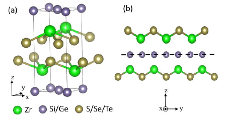
As mentioned above, the ZrXY compounds crystallize in the tetragonal structure [see Fig. 1(a)] with the P4/nmm (No. 129) nonsymmorphic space group which contains a glide mirror operation [Fig. 1(b)]. The experimental lattice constants used in the present calculations are listed in Table I. The electronic band structures are calculated based on the DFT with the generalized gradient approximation (GGA) to the exchange-correlation potential perdew1996generalized . The accurate full-potential projecter-augmented wave (PAW) methodblochl1994projector , as implemented in the Vienna ab initio simulation package (VASP) kresse1996efficient ; kresse1993ab , is used. The valence electronic configurations of Zr, Ge, Te, Si, S, Se taken into account are , , , , , and , respectively. A large plane wave cut-off energy of 400 eV is used. The self-consistent electronic band structure calculations are performed with a -centered -point mesh of 25 25 25 used in the Brillouin zone integration by the tetrahedron method jepson1971 ; Temmerman89 .
The intrinsic SHC is calculated within the Berry phase formalism guo2008intrinsic ; xiao2010berry . In this approach, the SHC () is simply given by the Brillouin zone (BZ) integration of the spin Berry curvature for all occupied bands,
| (1) |
| (2) |
where is the th component of spin current density, is the Fermi distribution, and is the spin Berry curvature for the band at k. and . is the spin direction, is the Pauli matrix, and is the velocity operator Guo05 . Similarly, the spin Nernst conductivity () can be written asxiao2010berry ; guo2017large
| (3) | ||||
In the SHC and SNC calculations, the velocity and spin velocity matrix elements are calculated from the self-consistent relativistic band structures within the PAW formalism Adolph01 , and the band summation and the BZ integration with the tetrahedron method are carried out by using a homemade program Guo14 ; guo2017large . A very fine -point mesh of 15498 k points in the IBZW is used, and this corresponds to the division of the line into intervals. Further test calculatons for ZrSiS using denser -point meshes of and 60 show that the calculated SHC and SNC converge within a few percent.
III RESULTS AND DISCUSSION
| System | ) | |||||||||
|---|---|---|---|---|---|---|---|---|---|---|
| (Å) | (Å) | (1/eV) | (/e)(S/cm-eV) | |||||||
| ZrSiS | 3.544a | 8.055a | 0.75 | 79 | -280 | -611 | -1229 | 0.60 | 0.52 | 1.51 |
| ZrSiSe | 3.623a | 8.365a | 0.47 | -26.6 | -452 | -556 | -3143 | 0.40 | 0.61 | 1.02 |
| ZrSiTe | 3.692a | 9.499a | 0.96 | -197 | -376 | -755 | 1141 | -0.80 | -0.76 | -0.60 |
| ZrGeS | 3.656a | 8.107a | 1.15 | 217 | -106 | -208 | -2624 | 0.39 | 0.29 | 0.54 |
| ZrGeSe | 3.706a | 8.271a | 0.76 | 182 | -247 | -486 | -1465 | 0.37 | 0.49 | 0.96 |
| ZrGeTe | 3.866a | 8.599a | 1.12 | 136 | -262 | -551 | -1064 | 0.53 | 0.48 | 1.17 |
| Mn3Sn (AF)b | – | – | 1.96 | 72 | – | – | -845 | 0.91 | – | – |
| Mn3Ga (FM)b | – | – | 6.82 | -678 | – | – | -10601 | 0.44 | – | – |
| fcc Pt | – | – | 1.75 | 2139c | – | – | 1214c | -1.09 (-0.91)b,-1.57d | – | – |
| TaAse | – | – | – | -781 | – | – | – | – | – | – |
aX-ray diffraction experiment Haneveld64 ; bAb initio calculation guo2017large ; cAb initio calculation guo2008intrinsic ; d Experiment at 255 K meyer2017observation ; eAb initio calculation sun2016strong .
| SHC | SNC | ||||
| x | y | z | x | y | z |
III.1 Electronic band structures
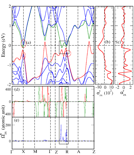
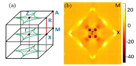
The six compounds of the ZrSiS-family studied in this paper all have a non-magnetic ground state. The calculated relativistic band structures are shown in Fig. 2(a) and Fig. 3(a) for ZrGeTe and ZrSiTe, respectively, and that of the other compounds are displayed in Figs. S1 - S6 in the Supplemental Material (SM)supp . The bands near the Fermi level, labeled in green and red, are mainly contributed by Zr -orbitals. Their semimetallic nature can be seen from the calculated low density of states (DOS) near the Fermi level, as listed in Table I. With the Kramers degeneracy given by the time-reversal symmetry together with the spatial inversion symmetry, all the compounds possess globally double degeneracy at every -point. Furthermore, two doubly degenerate bands would cross at time-reversal invariant momenta (TRIM) X and R under the protection of the glide mirror symmetry [Fig. 2(b)], thus forming a four-fold Dirac node at these -points. The Dirac nodes pinned at the TRIMs cannot be gapped by the SOC. The Dirac nodes at the X and R points are highlighted with the red circles in Figs. 2(a) and Fig. 3(a) as well as in Figs. S1-S6 in the SM supp . These are just the end points of the Dirac line-nodes along the X-R and A-M lines at the zone boundariesSu2018 ; chen2017dirac , which are protected by the glide mirror operation, as labeled by the red line in e.g., Fig. 4(a).
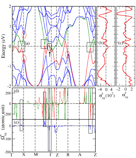
Unlike the nonsymmorphic symmetry-protected line nodes, the unprotected nodes along the -X, -M, Z-R, and Z-A would be gapped out because the symmetry has only one irreducible representation in the presence of the SOC. These gapped nodes can be seen from the calculated band structures in Fig. 2(a) and Fig. 3(a), where some of the gapped nodes are highligeted by the black boxes with the corresponding spin Berry curvature peaks displayed in Fig. 2(e) and Fig. 3(e). Interestingly, the gapped Dirac nodes along these high symmetry lines form a diamond-shaped loop on the -X-M plane and also the Z-R-A plane, as indicated by the green lines in Fig. 4(a). These nodal loop features in the band structures have been observed in the previous ARPES experimentsschoop2016dirac ; hosen2017tun ; nakamura2019evidence . Such diamond-shaped Fermi surface can also exhibit interesting properties such as large anisotropic magneto-resistance ali2016butterfly and the U-shape optical conductivity allah2019optical . In addition to the type-I Dirac nodes shared by the ZrSiS-family, ZrGeTe has interesting type-II Dirac points near the point just below the Fermi level, as indicated by the black arrow in Fig. 2(a). These type-II Dirac points become slightly gapped (the gaps are smaller than 0.0001 eV) when the SOC is taken into account.
III.2 Spin Hall effect
The SHC (; ) for a solid is a third-order tensor. However, for a highly symmetric crystal such as the ZrXY family, most of the tensor elements are zero. The nonmagnetic ZrXY family has space group P4/nmm, which corresponds to the magnetic Laue group 4/mmm1’. In Table II, the shape of the SHC tensor for the nonmagnetic ZrXY family, uncovered by a symmetry analysis seeman2015 , is displayed. Therefore, the nonmagnetic ZrXY family has only three nonzero elements, namely, , and . Note that the and here denote the [100], [010], and [001] directions, respectively, and hence the -direction is equivalent to the -direction. Consequently, and . In Table I, the calculated nonzero elements of the SHC of all six compounds are listed. The of some well studied systems such as noncollinear antiferromagnet Mn3Sn and ferromagnetic Mn3Gaguo2017large , platinum metal guo2008intrinsic ; meyer2017observation , and Weyl semimetal TaAs sun2016strong , are also listed in Table I for comparison.
In Table I, the results for the six compounds considered here are listed in the increasing order of their SOC strengths. Among them, ZrSiS has the weakest SOC strength while ZrGeTe has the strongest one. This is based on the well-known fact that the larger the atomic number of an element is, the stronger the SOC in the atoms of the element. The values of some nonzero elements of the SHC tensor in the six compounds can be large. In particular, the of ZrSiTe has the largest SHC value of -755 (/e)(S/cm). This SHC value is ten times larger than that [72 (/e)(S/cm)] of the noncollinear antiferromagnetic Mn3Sn guo2017large and also slightly larger than the SHC [72 (/e)(S/cm)] of the ferromagnetic Mn3Ga [-678 (/e)(S/cm)] guo2017large . Interestingly, this is close to the calculated value of the of TaAs sun2016strong , where the spin Hall response was found to mainly come from the anticrossing Weyl nodal lines gapped by the SOC, similar to the mechanism found here which will be illustrated below in the next subsection. Nonetheless, Table I indicates that the values of all nonzero elements of the SHC tensor in the six compounds are smaller than the SHC () of fcc platinum, which possesses the largest intrinsic SHC [2200 (/e)(S/cm)] among the transition metals guo2008intrinsic ; Guo14 . However, we expect that the members of the ZrSiS family with a large SHC would have a higher charge-spin current conversion efficiency than platinum. The spin Hall angle (), which is defined as the ratio of the SHC to the ordinary electric conductivity, is a widely used measure of this efficiency. Members of the ZrSiS family are semimetals and thus should have an electric conductivity much smaller than that of platinum. In particular, the in-plane conductivity of ZrSiTe at room temperature is about 10000 S/cm hosen2017tun , which is six times smaller than that (64000 S/cm) of platinumAndo08 . Thus, we can expect that the for ZrSiTe would be twice as large as that of platinum. Note that the conductivity along the axis (out-of-plane direction) in the ZrSiS family could be an order of magnitude smaller. Novak19
Interestingly, all six compounds exhibit a strong anisotropy in the spin Hall effect. In particular, Table I shows that the SHC of ZrSiSe could be increased by a factor of 20 if the spin polarization of the spin current is switched from the direction (perpendicular to the layers) to an in-plane direction (the or direction). Furthermore, in ZrGeY (Y = Te, Se, S), a rotation of the spin polarization direction from the axis to an in-plane direction would change the sign of the SHC (see Table I). Table I also indicates that the SHC depends strongly on the direction of the applied eiectric field. For example, the SHC of all the six compounds for the field applied along the [100] direction () is nearly two times larger than that along the [001] direction () (Table I). This large anisotropy in the SHE of the ZrSiS family could be attributed to their layered tetragonal structure with the four-fold rotational axis perpendicular to the layers (Fig. 1).
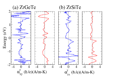
Since the SHC could be sensitive to the location of the Fermi energy (), we also calculate the SHC as a function of . In panel (b) of Fig. 2 and Fig. 3, the of ZrGeTe and of ZrSiTe are displayed as a function of , respectively, and that for the other nonzero elements are presented in Figs. S1-S6 in the SM supp . Indeed, as one can see from the figures, the SHC curves show a significant dependence on the . Interestingly, most of the SHC elements have a peak near the [see panel (b) in Figs. 2 and 3 as well as Figs. S1-S6 in the SM supp ]. As will be explained in the next subsection, this is due to the fact that there are a lot of Dirac nodal points and lines near the which are slightly gapped by the SOC in these Dirac semimetal compounds. In ZrSiTe, the prominent peak in the spectrum is located slightly below the (-0.08 eV) [see Fig. 3(b)], and thus, a small lowering of the could increase the from -755 to -850 (/e)(S/cm). This could be accomplished by hole-doping of 0.07 e/f.u via chemical substitution or electric gating.
III.3 Spin Berry curvature analysis
To understand the origin of the large SHC in some of the six compounds, let us now take a look at the band- and -resolved spin Berry curvatures for the bands near the Fermi level. According to Eq. (1), the SHC is simply given by the summation of spin Berry curvatures on the occupied bands only. Interestingly, it has been shown that when a band-crossing point such as a Dirac point becomes slightly gapped by the SOC, the spin Berry curvatures usually appear as a pair of peaks with opposite signs, respectively, on the upper and lower gapped bands in the vicinity of the -pointguo2008intrinsic . When both bands are occupied, the contributions to the SHC from these two peaks would cancel each other. However, when only one band is occupied or the falls within the gap, only one peak of spin Berry curvature would contribute to the SHC, thereby giving rise to a large SHC. Therefore, we show the calculated spin Berry curvatures and for the energy bands near the in ZrGeTe and ZrSiTe in Fig. 2(d) and Fig. 3(d), respectively. The total spin Berry curvatures which are a summation of the spin Berry curvatures of all the occupied bands below the Fermi level at each -point, are displayed in Fig. 2(e) and Fig. 3(e). The calculated spin Berry curvatures for the other cases are displayed in Figs. S1 - S12 in the SM supp .
Figure 2(a) shows that in the band structure of ZrGeTe, there are several gapped Dirac nodes near the along the symmetry lines in the Brillouin zone, as highlighted by the black boxes. These gapped nodes result in prominent spin Berry curvature peaks shown in Fig. 2(e). Interestingly, the largest negative peak near the point comes from the SOC-gapped type-II Dirac point. The relation between the large spin Berry curvatures and the Dirac nodes in the band structure can be seen more clearly from Fig. 4. Figure 4 (b) shows that the total spin Berry curvature ) positively peaks along the gapped nodal line loop in the -X-M plane [see the green diamond-shaped loop in Fig. 4 (a)]. Four large negative spin Berry curvature peaks near the from the gapped type-II Dirac points [see Fig. 2(a)] can also be seen in Fig. 4 (b). Similar situations occur in the other five considered ZrSiS-type compounds (see Figs. S1-S12 in the SMsupp ). There are many more spin Berry curvature peaks along the diamond-shaped nodal lines than on the single nodal points. Therefore, the large SHC values found in these Dirac semimetals originate mainly from the Dirac nodal lines.
Since there are many slightly gapped Dirac nodes near the Fermi level in the considered compounds [see panel (a) in Figs. 2 and 3 as well as Figs. S1-S12 in the SM supp ], one can imagine that a small variation of the Fermi level could significantly change the SHC, as demonstrated in panel (b) of Figs. 2-3 and also of Figs. S1-S6 in the SM supp . Interestingly, this woud allow one to optimize the SHE in these Dirac semimetals by, e.g., chemical doping. A surprisingly finding here is that the symmetry-protected nodes (degeneracies) can also generate large spin Berry curvatures, which would form an antisymmetric butterfly-like shape on the two sides of the crossing point [see, e.g., the inset in Figs. S7(a) and S8(a) in the SM supp ]. Here along the high -symmetry -Z line, the band crossing due to a band inversion is allowed. For example, Fig. S7(a) shows that in ZrGeTe, a symmetry-protected crossing exists along the -Z, due to the band inversion between bands and bands. The interesting shape of the peaks can be understood in terms of Eq. (2) as follows. When the order of and is inverted on either side of the crossing point, a sign change in the spin Berry curvature would occur, as can be see from Eq. (2). Nonetheless, since these symmetry-protected Dirac nodes are well below the Fermi level, they are not expected to contribute significantly to the SHC.
III.4 Spin Nernst effect
The SNC () for a solid is also a third-order tensor. Since the transverse spin currents generated by a longitudinal electric field and a longitudinal temperature gradient have the same transformation properties under the symmetry operations, the shape of the SNC is identical to that of the SHC seeman2015 , as displayed in Table II. Therefore, the SNC of the nonmagnetic ZrXY family also has only three nonzero elements of , , and . Table I shows that the calculated values of the nonzero elements of the SNC tensor of the six compounds are significant. In fact, the of ZrGeTe and ZrSiS are even larger than the of platinum (Table I). Therefore, these findings suggest that the DSMs of the ZrSiS-family can serve as promising candidate materials for spintronics and spin caloritronics due to their efficient charge-spin current conversion driven by heat.
As for the SHC, the SNC of the six compounds is significantly anisotropic. For example, Table I shows that the SNC of ZrGeTe for the spin polarization of the spin current along the axis () is about half of that for the spin polarization along the axis (). Furthermore, the SNC of ZrGeTe for the electric field applied in the [100] direction () is two times larger than that in the [001] direction (). Nevertheless, in contrast to the SHC, the SNC in ZrGeY (Y = Te, Se, S) does not change sign when the spin polarization of the spin current is rotated from the axis to the or axis (Table I).
We also calculate the SNC as a function of . In panel (c) of Fig. 2 and Fig. 3, the of ZrGeTe and of ZrSiTe are displayed as a function of , respectively. For the other compounds, the corresponding SNC curves are presented in Figs. S1-S6 in the SM supp . These figures suggest that the SNC has a stronger dependence than the SHC. For instance, the of ZrGeTe increases rapidly as the increases up to 0.06 eV where it reaches the local maximum of 1.0 (/e)(A/m-K). As the further increases, it decreases steadily and changes sign at 0.14 eV and then reaches the negative local maximum of -0.93 (/e)(A/m-K) at 0.21 eV[see Fig. 2(c) and also Fig. S1(c)]. Remarkably, as the rises, the of ZrSiS decreases steeply, changes sign at 0.05 eV, and then reaches the negative local maximum of 1.99 (/e)(A/m-K) at 0.10 eV, just slightly above the Fermi level [see Fig. S6(c) in supp ]. A similar behavior is found for the of ZrSiSe [Fig. S5(c) in supp ]. On the other hand, the of ZrSiTe would change sign and then become as large as 2.15 (/e)(A/m-K) when the is lowered to -0.23 eV [see Figs. 3(c) ánd 5(b) as well as Fig. S4(c) in supp ]. Again, these interesting phenomena could be observed in these compounds by chemical doping or electric gating.
In order to understand the origin of the prominent features in the spectrum of the SNC as a function of , we note that in the low temperature limit, Eq. (3) can be written as the Mott relation,
| (4) |
which indicates that the SNC is proportional to the energy derivative of the SHC
at the . In other words, a peak in the SNC would occur when the SHC
has a steep slope. In Table I, the energy derivatives of the at the
for the six compounds are listed, and they agree in sign
with the [note the minus sign in Eq. (4)].
In Fig. 5(a) [5(b)], the [] estimated
using the calculated []
and the Mott relation [Eq. (4)] (the blue curves) for ZrGeTe [ZrSiTe] is displayed together
with the SNC calculated from the relativistic band structure using Eq. (3) (the red curves)
(See Fig. S13 in the SM supp for the other four compounds).
Figure 5 and Fig. S13 show that most of the prominent peaks in the SNC are reproduced
by the Mott relation, suggesting that these peaks stem from the large energy-derivatives of the corresponding SHC.
Note that the rapid oscillations of the SNC derived from the Mott relation, e.g.,
around 2.0 eV in Fig. 5, are due to the uncertainties in the numerical differentiation
of the small oscillations in the SHC.
Consequently, the plateau feature in the SNC between and -1.0 eV in ZrGeSe, ZrGeS, ZrSiSe,
and ZrSiS can be understood as a result of the rather non-dispersive SHC within the same energy range,
where few gapped Dirac points exist. Similar to the SHC, the SNC values for these six compounds
can be optimized by slightly tuning the Fermi level via, e.g., chemical substitution.
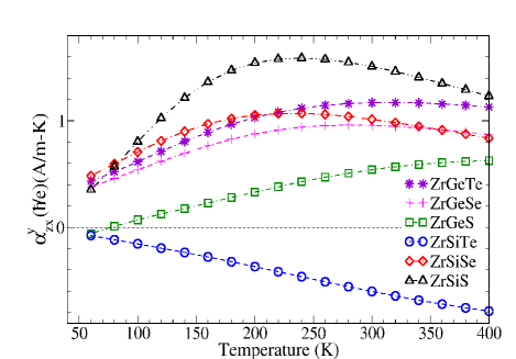
We also calculate the SNC as a function of temperature (). The -dependences of the for the six considered compounds are shown in Fig. 6 and that of the other nonzero elements are presented in Fig. S14 in the SM supp . Figure 6 shows that ZrSiS has the largest for K. The of ZrSiS reaches the maximum of 1.6 [()(A/mK)] at K and then decreases monotonically as further increases. Interestingly, the values of ZrGeTe, ZrGeSe, and ZrSiSe are very close and have a very similar behavior, i.e., they all increase monotonically as goes from 60 K, and then converge to similar values up to K (Fig. 6). In contrast, the of ZrGeS is negative at K and then changes sign at K. As further increases, it increases monotonically up to 400 K. We notice that the of ZrGeS exhibit an almost identical behavior to that of [see Fig. 6 and Figs. S14(b) in the SM supp ]. The , and of ZrSiTe are negative in the entire considered temperature range and decrease monotonically with temperature [see Fig. 6 and Figs. S14(b) in the SM supp ]. We note that the behavior of the other two nonzero SNC elements ( and ) of ZrSiTe are very similar (see Figs. S14 in the SM supp ).
IV CONCLUSIONS
In summary, we have thoroughly studied the SHE and SNE in Dirac nodal-line semimetals ZrXY (X = Si, Ge; Y = S, Se, Te) by performing systematic ab initio calculations within the Berry phase formalism. The calculated SHC and SNC of the six considered materials are large. In particular, the calculated SHC of ZrSiTe is as large as -755 [()(S/cm), being smaller but in the same order of magnitude of that of platinum, which posseses the largest intrinsic SHC among the metals. However, since the ZrSiS semimetals have a much smaller electric conductivity, they are expected to have a larger spin Hall angle than platinum. The calculated SNC of ZrSiS is = 1.51 ()(A/mK), being even larger than that of platinum. More importantly, it is found that both the amplitude and sign of the SHC and SNC of these compounds can be significantly manipulated by tuning the direction of the applied electric field or spin current, and also can be optimized by slightly varying the Fermi level via, e.g., chemical doping. This indicates that these materials can be useful materials for spintronics and spin caloritronics. Furthermore, the calculated band- and -resolved spin Berry curvatures reveal that the large SHE and SNE in these compounds and their remarkable tunabilities originate from the large number of Dirac nodal points and lines in the vicinity of the Fermi level. In the presence of the SOC, these Dirac nodes are slightly gapped, resulting in large spin Berry curvatures, and thus make major contributions to the SHC and SNC. This work is thus expected to stimulate further experimental investigations such as spin-related transport measurements on these interesting materials.
ACKNOWLEDGMENTS
The authors acknowledge the support from the Ministry of Science and Technology, the Ministry of Education, the National Center for Theoretical Sciences, and the Academia Sinica of the R. O. C. The authors also thank Dr. Tien-Ming Chuang for valuable discussion on the electronic structures of the ZrSiS-type compounds and Mr. Tzu-Cheng Wang for helpful communications on the electronic structure calculation of ZrSiS.
References
- (1) M. Switkes, C. Marcus, K. Campman, and A. Gossard, An Adiabatic Quantum Electron Pump, Science 283, 1905 (1999).
- (2) M. Z. Hasan and C. L. Kane, Colloquium: Topological insulators, Rev. Mod. Phys. 82, 3045 (2010).
- (3) L. Liu, A. Richardella, I. Garate, Y. Zhu, N. Samarth, and C.-T. Chen, Spin-polarized tunneling study of spin-momentum locking in topological insulators, Phys. Rev. B 91, 235437 (2015).
- (4) M. D’yakonov, Spin orientation of electrons associated with the interband absorption of light in semiconductors, Sov. Phys. JETP 33, 1053 (1971).
- (5) J. Hirsch, Spin Hall Effect, Phys. Rev. Lett. 83, 1834 (1999).
- (6) S. Murakami, N. Nagaosa, and S.-C. Zhang, Dissipationless quantum spin current at room temperature, Science 301, 1348 (2003).
- (7) J. Sinova, D. Culcer, Q. Niu, N. A. Sinitsyn, T. Jungwirth, and A. H. MacDonald, Universal Intrinsic Spin Hall Effect, Phys. Rev. Lett. 92, 126603 (2004).
- (8) Y. K. Kato, R. S. Myers, A. C. Gossard, and D. D. Awschalom, Observation of the spin Hall effect in semiconductors, Science 306, 1910 (2004).
- (9) G. Y. Guo, Y. Yao and Q. Niu, Ab initio Calculation of the Intrinsic Spin Hall Effect in Semiconductors, Phys. Rev. Lett. 94, 226601 (2005).
- (10) S. O. Valenzuela and M. Tinkham, Direct electronic measurement of the spin Hall effect, Nature (London) 442, 176 (2006).
- (11) A. Hoffman, Spin Hall Effects in Metals, IEEE Trans. Magn. 49, 5172 (2013).
- (12) J. Sinova, S. O. Valenzuela, J. Wunderlich, C. Back, and T. Jungwirth, Spin Hall effects, Rev. Mod. Phys. 87, 1213 (2015).
- (13) S. Cheng, Y. Xing, Q.-F. Sun, and X. C. Xie, Spin Nernst effect and Nernst effect in two-dimensional electron systems, Phys. Rev. B 78, 045302 (2008)
- (14) S. Meyer, Y.-T. Chen, S. Wimmer, M. Althammer, T. Wimmer, R. Schlitz, S. Geprägs, H. Huebl, D. Ködderitzsch, H. Ebert, G. E. W. Bauer, R. Gross, and S. T. B. Goennenwein, Observation of the spin Nernst effect, Nat. Mater. 16, 977 (2017).
- (15) P. Sheng, Y. Sakuraba, Y.-C. Lau, S. Takahashi, S. Mitani, and M. Hayashi, The spin Nernst effect in tungsten, Sci. Adv. 3, e1701503 (2017).
- (16) G.-Y. Guo, S. Murakami, T.-W. Chen, and N. Nagaosa, Intrinsic Spin Hall Effect in Platinum: First-Principles Calculations, Phys. Rev. Lett. 100, 096401 (2008).
- (17) D. Xiao, M.-C. Chang, and Q. Niu, Berry phase effects on electronic properties, Rev. Mod. Phys. 82, 1959 (2010).
- (18) G.-Y. Guo and T.-C. Wang, Large anomalous Nernst and spin Nernst effects in the noncollinear antiferromagnets Mn3X (X=Sn, Ge, Ga), Phys. Rev. B 96, 224415 (2017); Phys. Rev. B 100, 169907 (E) (2019).
- (19) A. Mellnik, J. Lee, A. Richardella, J. Grab, P. Mintun, M. H. Fischer, A. Vaezi, A. Manchon, E.-A. Kim, N. Samarth, and D.C. Ralph, Spin-transfer torque generated by a topological insulator, Nature 511, 449 (2014).
- (20) A. Burkov, M. Hook, and L. Balents, Topological nodal semimetals, Phys. Rev. B 84, 235126 (2011).
- (21) N. Armitage, E. Mele, and A. Vishwanath, Weyl and Dirac semimetals in three-dimensional solids, Rev. Mod. Phys. 90, 015001 (2018).
- (22) S. M. Young and C. L. Kane, Dirac Semimetals in Two Dimensions, Phys. Rev. Lett. 115, 126803 (2015).
- (23) L. M. Schoop, M. N. Ali, C. Straßer, A. Topp, A. Varykhalov, D. Marchenko, V. Duppel, S. S. Parkin, B. V. Lotsch, and C. R. Ast, Dirac cone protected by non-symmorphic symmetry and three-dimensional Dirac line node in ZrSiS, Nat. Commun. 7, 11696 (2016).
- (24) C. L. Kane and E. J. Mele, Quantum Spin Hall Effect in Graphene, Phys. Rev. Lett. 95, 226801 (2005).
- (25) C. L. Kane and E. J. Mele, Z2 Topological Order and the Quantum Spin Hall Effect, Phys. Rev. Lett. 95, 146802 (2005).
- (26) Y. Sun, Y. Zhang, C.-X. Liu, C. Felser, and B. Yan, Dirac nodal lines and induced spin Hall effect in metallic rutile oxides, Phys. Rev. B 95, 235104 (2017).
- (27) Y. Sun, Y. Zhang, C. Felser, and B. Yan, Strong Intrinsic Spin Hall Effect in the TaAs Family of Weyl Semimetals, Phys. Rev. Lett. 117, 146403 (2016).
- (28) J. Hu, Z. Tang, J. Liu, X. Liu, Y. Zhu, D. Graf, K. Myhro, S. Tran, C. N. Lau, J. Wei, and Z. Mao, Evidence of Topological Nodal-Line Fermions in ZrSiSe and ZrSiTe, Phys. Rev. Lett. 117, 016602 (2016).
- (29) M. M. Hosen, K. Dimitri, A. Aperis, P. Maldonado, I. Belopolski, G. Dhakal, F. Kabir, C. Sims, M. Z. Hasan, D. Kaczorowski, T. Durakiewicz, P. M. Oppeneer, M. Neupane, Observation of gapless Dirac surface states in ZrGeTe, Phys. Rev. B 97, 121103 (2018).
- (30) C.-C. Su, C.-S. Li, T.-C. Wang, S.-Y. Guan, R. Sankar, F. C. Chou, C.-S. Chang, W.-L. Lee, G.-Y. Guo, and T.-M- Chuang, Surface termination dependent quasiparticle scattering interface and magneto-transport study on ZrSiS, New J. Phys.20, 103025 (2018).
- (31) M. N. Ali, L. M. Schoop, C. Garg, J. M. Lippmann, E. Lara, B. Lotsch, and S. S. Parkin, Butterfly magnetoresistance, quasi-2D Dirac Fermi surface and topological phase transition in ZrSiS, Sci. Adv. 2, e1601742 (2016).
- (32) J. Hu, Y. Zhu, D. Graf, Z. Tang, J. Liu, and Z. Mao, Quantum oscillation studies of the topological semimetal candidate ZrGeM(M=S,Se,Te), Phys. Rev. B 95, 205134 (2017).
- (33) A. J. K. Haneveld and F. Jellinek, Zirconium silicide and germanide chalcogenides preparation and crystal structures, Recueil des Travaux Chimiques des Pays‐Bas 83, 776 (2017).
- (34) J. P. Perdew, K. Burke, and M. Ernzerhof, Generalized Gradient Approximation Made Simple, Phys. Rev. Lett. 77, 3865 (1996).
- (35) P. E. Blöchl, Projector augmented-wave method, Phys. Rev. B 50, 17953 (1994).
- (36) G. Kresse and J. Furthmüller, Efficient iterative schemes for ab initio total-energy calculations using a plane-wave basis set, Phys. Rev. B 54, 11169 (1996).
- (37) G. Kresse and J. Hafner, Ab initio molecular dynamics for liquid metals, Phys. Rev. B 47, 558 (1993).
- (38) O. Jepson and O. Anderson, The electronic structure of h.c.p. Ytterbium, Solid State Commun. 9, 1763 (1971).
- (39) W. M. Termmerman, P. A. Sterne, G. Y. Guo and Z. Szotek, Electronic Structure Calculations of High Tc Materials, Molecular Simulations 4, 153 (1989).
- (40) B. Adolph, J. Furthmüller and F. Beckstedt, Optical properties of semiconductors using projector-augmented waves, Phys. Rev. B 63, 125108 (2001).
- (41) G. Y. Guo, Q. Niu and N. Nagaosa, Anomalous Nernst and Hall effects in magnetized platinum and palladium, Phys. Rev. B 89, 214406 (2014).
- (42) See Supplemental Material at http://link.aps.org/supplemental/10.1103/PhysRevB for supplementary Figs. S1 - S14.
- (43) C. Chen, X. Xu, J. Jiang, S.-C. Wu, Y. Qi, L. Yang, M. Wang, Y. Sun, N. Schröter, H. Yang, L. M. Schoop, Y. Y. Lv, J. Zhou, Y. B. Chen, S. H. Yao, M. H. Lu, Y. F. Chen, C. Felser, B. H. Yan, Z. K. Liu, and Y. L. Chen, Dirac line nodes and effect of spin-orbit coupling in the nonsymmorphic critical semimetals MSiS (M=Hf,Zr), Phys. Rev. B 95, 125126 (2017).
- (44) M. M. Hosen, K. Dimitri, I. Belopolski, P. Maldonado, R. Sankar, N. Dhakal, G. Dhakal, T. Cole, P. M. Oppeneer, D. Kaczorowski, F.-C. Chou, and M. Z. Hasan, Tunability of the topological nodal-line semimetal phase in ZrSiX-type materials (X=S, Se, Te), Phys. Rev. B 95, 161101 (2017).
- (45) T. Nakamura, S. Souma, Z. Wang, K. Yamauchi, D. Takane, H. Oinuma, K. Nakayama, K. Horiba, H. Kumigashira, T. Oguchi, T. Takahashi, Y. Ando, and T. Sato, Evidence for bulk nodal loops and universality of Dirac-node arc surface states in ZrGeXc (Xc=S, Se, Te), Phys. Rev. B 99, 245105 (2019).
- (46) J. Ebad-Allah, J. F. Afonso, M. Krottenmüller, J. Hu, Y. L. Zhu, Z. Q. Mao, J. Kuneš, and C. A. Kuntscher, Chemical pressure effect on the optical conductivity of the nodal-line semimetals ZrSiY (Y= S, Se, Te) and ZrGeY (Y= S, Te), Phys. Rev. B 99, 125154 (2019).
- (47) M. Seemann, D. Kodderitzsch, S. Wimmer, and H. Ebert, Symmetry-imposed shape of linear response tensors, Phys. Rev. B 92, 155138 (2015).
- (48) K. Ando, S. Takahashi, K. Harii, K. Sasage, J. Ieda, S. Maekawa and E. Saitoh, Electric manipulation of spin relaxation using the spin Hall effect, Phys. Rev. Lett. 101, 036601 (2008).
- (49) M. Novak, S. N. Zhang, F. Orbanic, N. Biliskov, G. Eguchi, S. Paschen, A. Kimura, X. X. Wang, T. Osada, K. Uchida, M. Sato, Q. S. Wu, O. V. Yazyev, and I. Kokanovic, Highly anisotropic interlayer magnetoresistance in ZrSiS nodal-line Dirac semimetal, Phys. Rev. B 100, 085137 (2019).