On the Homogeneity of TiN Kinetic Inductance Detectors
Produced through Atomic Layer Deposition
Abstract
The non-homogeneity in the critical temperature of an Microwave Kinetic Inductance Detector (MKID) could be caused by non-uniformity in the deposition process of the thin superconducting film. This produces low percent yield and frequency collision in the readout of the MKIDs. Here, we show the homogeneity that offers Atomic Layer Deposition (ALD). We report an improvement of up to a factor of 50 in the fractional variation of the for TiN MKIDs fabricated with Atomic Layer Deposition in comparison with MKIDs fabricated with sputtering. We measured the critical temperature of 48 resonators. We extracted the of the MKIDs by fitting the fractional resonance frequency to the complex conductivity of their resonators. We observed uniformity on the critical temperature for MKIDs belonging to the same fabrication process, with a maximum change in the of 60 mK for MKIDs fabricated on different wafers.
I INTRODUCTION
MKIDs belongs to non-equilibrium superconducting devices, which principle of operation is based on the measurement of the electrodynamic response of the superconductor, by a change in the kinetic inductance when a photon is absorbedNon-equilibrium . The MKID has attractive features like high quantum efficiency, low theoretical noise limit, multiplex frequency domain, photon-number-resolving and energy resolvingGuo:2017ukv .
The MKID arrays designed for various instruments share many common structures. Usually, these structures include superconducting LC resonators (capacitor and inductor), transmission lines and antennas (See Figs. 2 and 3). The superconducting resonators (pixels) are the photon detectors, which active area consists of a meandered inductor that acts as the photosensor and an interdigitated capacitor (IDC).
The production process of an MKID consists of depositing a superconducting thin film on an insulating substrate and applying standard lithographic patterning techniques to produce a resonator structure. These simple single-layer structures permit the use of high-quality crystalline substrates and a wide variety of superconducting films, providing an opportunity to achieve extremely low dissipation, desirable for precision instruments.
One of the most important features of the MKIDs is their capability to multiplex into large arrays. This capability enables the MKIDs to be used as powerful new astrophysical instruments for ground and space arrays besides of an extensive variety of applications. For example, one of the first MKIDs built for a camera is found in the experiment ARCONS Arcons2024 . In SuperSpecSuperscpec , it is used as a component of a spectrograph, in the OlimpoOLIMPO_MKIDs experiment to study the Cosmic Microwave Background (CMB) and recently, the use of MKIDs has been growing as an element of readout for QubitsSQUID_1 ; SQUID_2 ; SQUID_3 ; SQUID_4 . In addition, the MKIDs have been proposed as WIMP dark matter detectors WIMPMKIDS and as devices for measuring the neutrino mass OLIMPO_MKIDs .
In spite of the advantage that the MKIDs provides to readout thousand of resonators coupled to one transmission line, in some cases, the MKIDs present problems such as non-uniformity, instability, low percent yield and frequency collisions between their resonators. These problems are usually believed to be associated with the process of depositionSzypryt:2014eua .
In this sense, we are investigating ways to increase the homogeneity in the deposition to improve the per pixel performance of our devices through new superconducting material systems and fabrication techniques. The route that we are currently exploring attempts to create more uniform films through the use of Atomic Layer Deposition rather than the more traditional sputtering method. ALD is a thin-film technique based on the sequential use of a gas phase chemical process. Some of the advantages that offer the use of ALD are the thickness and composition controlATOMIC_HYSTORY . The superconducting material selected is TiN, whose is usually below 6K TiN_6K_Tc . The critical temperature of the TiN depends on the thicknessTc_Thicknees_1 ; Thicknes_2 or the N2 concentrationTiN_6K_Tc ; Tc_by_N2_1 ; Tc_by_N2_2 . Therefore, through the measurement of the critical temperature, we will assess the uniformity of ALD.
In this paper will discuss the uniformity of ALD by measuring the critical temperature of 48 resonators coming from four identical MKIDs. All the MKIDs were fabricated with deposition of TiN through Atomic Layer Deposition under the same conditions. The is extracted fitting the fractional resonance frequency change to some analytical expressions of the complex conductivity given by the Mattis-Bardeen theory. Finally, the reproducibility of the fabrication is investigated by measuring and comparing the resonance frequency , loaded quality factor, and kinetic inductance of each resonator, where the variations are tried to explain through simulations of some fabrication processes.
II Superconducting Resonators
In a.c. current, the Cooper pairs of a superconductor are accelerated storing energy in the form of kinetic energy. The energy is stored inside the superconductor a short distance ( 50 nm) in the form of a magnetic field. This effect is added to the surface impedance of the superconducting material, where describes a.c losses at angular frequency caused by electrons that are not in Cooper pairs and is the surface inductance due to the reactive energy flow between the superconductor and the electromagnetic field BASELMANS2007708 ; CalibrationwithNqp . The in a resonant circuit is the inductive element, which is a function of the temperature-dependent kinetic inductance KineticInductance , which is inversely proportional to the critical temperature of the superconducting material .
The resonance frequencySimon_Doyle_Thesis of the resonant circuit as a function of the kinetic inductance is given by
| (1) |
where is the geometrical capacitance and is the geometrical inductance.
The critical temperature of a resonator can be obtained by fitting the fractional resonance frequency change to the imaginary part of the complex conductivity of a superconductor Aluminum . The fractional resonance frequency change can be expressed as
| (2) |
where is the ratio of the kinetic inductance and the total inductance of the resonator GAO2006585 , and is the imaginary part of the complex conductivity, which has the following analytical approximate expression according to the Mattis-Bardeen theoryAluminum ; Simon_Doyle_Thesis
| (3) |
Here is the normal conductivity, is the 0-th order modified Bessel function, is the frequency of the a.c. and is the energy gap of the superconductor.
In TiN films it has been shown that the complex conductivity increasingly deviates from conventional Mattis-Bardeen theory due to a strongly disorder of TiN DisorderedTiN . This phenomenon is observed in Fig. 10. However, the critical temperature of the superconductor is not affected by the disorderDIRTYSUPERCONDUCTORS and we can consider that the is fixed in all resonators. Therefore, we expect the same value of as a function of the temperature in all resonators.
We are using microwave techniques to obtain the resonance frequency of each resonator. The complex transmission amplitude of a resonator obtained from the network analyzer is fitted to the model of the total transmission Analysimethodgoodfunction ; Besedin2018 ; COMPLEXSACATTERINGDATTA of a notch type resonator coupled to the transmission line, given by
| (4) |
The coupling is via a Coplanar Waveguide (CPW) to covey microwave frequency signals. The geometrical dimension of the central strip and ground planes are shown in Fig. 3. The term takes impedance mismatches which are caused by an asymmetry in the transmission amplitude. and are the loaded quality factor and the coupling quality factor of a resonator, respectively (see Appendix A).
III Design, fabrication and simulation
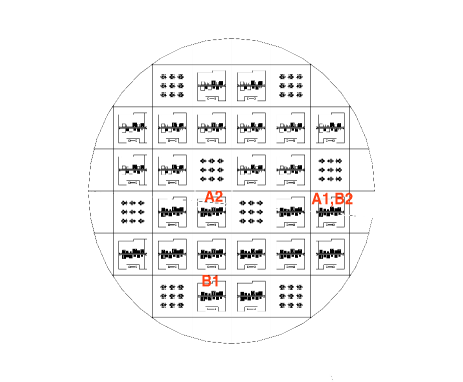
We fabricated 24 identical MKIDs, containing 12 resonators each, in two Si wafers. 12 were fabricated in one wafer and the other 12 in another wafer. The 12 MKIDs were fabricated in the bottom half of the wafers. The upper half contains other kinds of MKIDs and stuff that were not used on this work. The production yield of MKIDs was of 100% in both wafers. Whereby, all MKIDs could be mounted and useful.
We report on the comparison of four of these MKIDs, 2 from each wafer, which we will refer to A1, B1 (from wafer 1) and A2, B2 (from wafer 2). The position of these MKIDs on the wafers is shown in Fig. 1 (as they are identical, the two wafers are shown in the same figure).
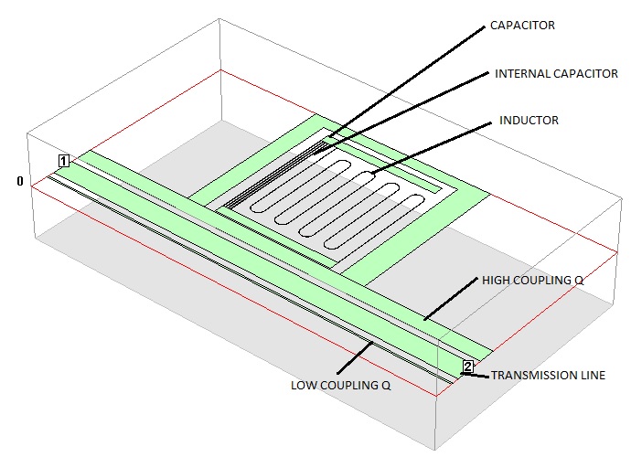
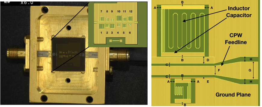
The base pixel design is shown in Figs. 2 and 3. It consists of one inductor in parallel with a capacitor that contains an internal interdigitated part. The system is surrounded by a ground plane that is part of a coplanar waveguide. One part of the capacitor is close to the CPW feedline and is thus coupled to the CPW.
Fig. 3 shows a picture of an MKID in its package. The inset shows the array of 12 pixels, with different sizes. Each of the 12 resonators on an MKID was designed to have a unique resonant frequency. Six pixels (labelled 1–6) are coupled to the CPW feedline through a thick conducting stripe, providing a high quality factor . The other six pixels (7–12) are coupled to the transmission line through a thin stripe, providing a low .
The right-hand side of Fig. 3 shows the details of the geometry of two resonators and the CPW. The separation with respect to the ground plane is identical for each pixel, and (see the labels in the figure). The CPW line is separated from the two ground planes by a distance . The separation of the capacitors to the CPW line varies according to the expected strength of the coupling, reflecting on the value of . For the resonators we have , whereas for the low ones we have . The width of the feedline across the resonators is , broadening to on the extremities, with a separation to the ground planes of .
The MKIDs fabrication was performed at University of Chicago’s Pritzker Nanofabrication Facility. The fabrication process involved three main steps: i) the deposition of 300 layers of TiN on a 125 mm Si wafer (using the Ultratech/Cambridge Fiji G2 Plasma-Enhanced ALD equipment), ii) the imprint of the circuits using maskless lithography (with the Heidelberg MLAD150 Direct Write Lithographer), and iii) the removal of the excess TiN through dry etching (employing the Plasma-Therm ICP Chlorine Etch). The chosen ratio of the TiN and Si etch rates was 1:2. The deposited layers of TiN correspond to a thickness of 25 nm, which was chosen so that the expected superconducting transition temperature is about 4.1K.
Each of the four MKIDs was packaged in a separate gold-plated copper box (see Fig. 3) with 50 SMA ports and each was mounted and tested under the same conditions. The copper box was mounted on the cold stage of a two-stage adiabatic demagnetization refrigerator (ADR). The stage was cooled to 103 mK. The input and output were connected to a vector network analyzer (VNA) which sent a -40 dB signal to the MKID. The signal is amplified by a cryogenic High Electron Mobility Transistor (HEMT) amplifier.
We simulated the 12 resonators previous to the fabrication to know their resonance frequencies, load quality factors, geometrical capacitance and geometrical inductance. The simulations of each of the 12 resonators are done separately in SONNET. Fig. 2 shows the geometry used for the simulation of one resonator. The input parameters for the 12 resonators were the same. The stackup from bottom to top, was 500 silicon (Erel = 11.7) beneath 1000 air (Erel = 1). The metallization on top of the silicon layer was TiN (surface resistance = 0, thickness = 0, and the kinetic inductance swept from 15 pH/sq to 40 pH/sq in steps of 2 pH/sq). There was a 50 port on each end of the transmission line. From the simulation, we obtain the complex transmission amplitude (Figs. 8 and 9) and by doing a fit to equation (4), extracted the resonance frequency and loaded quality factor . Using and , and were obtained by a fit to equation (1). The resonance frequency span of the 12 resonators ranged from 0.5 GHz to 4.5 GHz for kinetic inductance sweep from 15 pH/sq to 40 pH/sq. The loaded quality factors of the 12 resonators can be divided in two groups: six resonators with low and six resonators with high .
IV Measurements
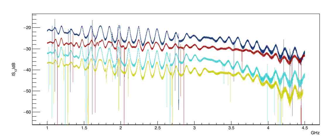
In Fig. 4 we show the transmission curves for the four MKIDs obtained at 103 mK and -40 dB. From top to bottom: A1 (blue), B1 (red), A2 (cyan), and B2 (yellow). The resonance frequencies are seen as sharp spikes in this plot. The oscillations and overall shape of the curve are due to the transmission line. The first 10 resonance frequencies are in the range 1–3 GHz and the other two from 4 GHz to 4.5 GHz. The spikes in the range from 3–4 GHz correspond to second modes of the resonance frequencies, as identified in the simulations.
Analyzing the resonance frequencies, from the four MKIDs A1, A2, B1, B2, we can identify the twelve resonance frequencies in the range 1-4.5 GHz (Fig. 4) similar to the simulation, where the MKID A2 contains the lower in all its resonators.
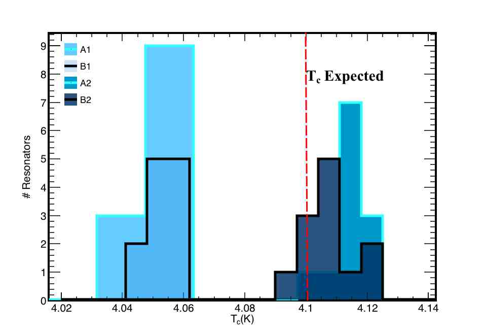
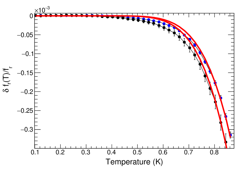
To verify the uniformity of ALD we proceed to extract the with the method proposed in Appendix B for all resonators. Fig. 5 shows a distribution of critical temperature of all resonators where we can see four distributions close to the expected critical temperature. The MKIDs from the first wafer correspond to the left-most distributions and the ones from the second wafer correspond to the right-most distributions. The critical temperature averages are 4.05 K, 4.05 K for B1, A1 and 4.11 K, 4.10 K for A2, B2, respectively.
Calculating the average differences in the critical temperature for the 4 MKIDs (taking as reference the MKID B1) and dividing between the maximum sigma error , we obtain values of of 0.76 and 0.91 for A1-B1 and A2-B2, respectively.
To investigate if the value of is constant and independent of the function used to do the fit, we considered different functionsSuperconductingTiN ; GaOthesis to fit the and obtained . We found that the distribution of the critical temperatures shown in Fig. 5 is the same for all the proposed functions, just varying in the mean , and the values of . This shows that the MKIDs from the same wafer have the same .
The percent variations in the critical temperature achieved in sputtering for MKIDs of TiNTiNCriticalMultilayers ; TcSputtering are of the order of 25% and, in our case, the percent variation of A1-B1 and A2-B2 is 0.3% and 0.5% respectively. This shows that ALD leads to a better control in the critical temperature, even with MKIDs from different wafers, where the percent variation obtained is (1.9%).
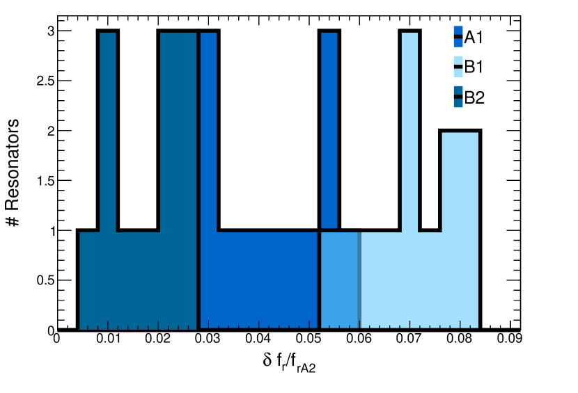
Notwithstanding this low percent variation, it is obtained a high variation in the resonance frequency (Fig. 6) and a discrepancy in the loaded quality factor (Fig. 7).
The fractional change of the resonance frequency (comparing the resonators 1,..,12 from the MKID A2 with the resonators 1,..,12 from the MKID A1, B1, B2) is plotted in a histogram (Fig. 6). The fractional differences are rather small (less than 10%), being less than 2.6% for the 2 MKIDs from wafer and less than 3.3% for those from wafer 2. The maximum change found in for A1-B1 is and for A2-B2 is . These values are higher in comparison with the value reported of for identical resonators of TiN built through sputteringV_D_F_R_0 (the resonators are on the same wafer and same MKID).
To verify if the changes of the resonance frequencies are a consequence of the variation of the critical temperature, we analyze the local kinetic inductance of all 48 resonators through the methods of Appendix C. In the case of the local kinetic inductance the values are between 18 pH/sq and 24 pH/sq (Fig. 11), where each resonator has a unique value of . Calculating the global kinetic inductance using equation (8), the values are 19.5 pH/sq, 20.4 pH/sq, 21.5 pH/sq, 22.13 pH/sq for B1, A1, B2, A2, respectively. Then, we obtained a change in of 0.5 K for A1 respect to A2 and 0.1 K for A1,B1 and A2,B2 considering that . Those values are bigger in comparison with the expected values obtained through the fit to the fractional resonance frequency change, given in table 2. Therefore, the variation in the resonance frequency could be due to other factors such as the variation in the losses of the system and in the over-etch into silicon V_D_F_R_0 .
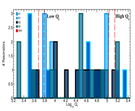
In a resonator the losses of the system are counted by the loaded quality factor . From Fig. 7 it is clear that each resonator has a different , and in the half of them its value is below the one obtained from the simulation. The fact that the loaded quality factor results lower than the simulated value indicates that there are more losses in the system. These could be by the wire bonding, the connection with the ports and other external agents. In contrast, the values above the designed value could be produced by the CPW line. If we observe the Fig. 4 the variation of the dB presented in the baseline is produced by a mismatch with the CPW line and its connections.
In order to explain any possible process involved in the fabrication stages, we performed three simulations, changing, 1) the area of the resonators by 10% (including the CPW and all the components), 2) the dielectric permeability of the substrate (from 68% to 171%) and 3) the non-homogeneity of the etch (depth from 0 to 150 ). In all the simulations the kinetic inductance used was 21 pH/sq and, in 2) and 3) the Erel was taken as 11.7.
The simulation 1) shows a change of 9% in and MHz in . In 2), varies from 128% to 76% and from 233 MHz to -213 MHz. Finally, 3) shows a decrease in of 50% for 10 and 24% for 150 , and the resonance frequency changed from 1.1 GHz to 2.24 GHz. All these simulations represent extreme cases and the changes considered are way above the specifications of all the processes involved in the fabrication. For example, the reported purity of Si is around 99.99% SiliconBOOk , which mean that the permeability can change by at most 0.001%.
V Conclusions
We have demonstrated the uniformity of Atomic Layer Deposition through measuring the critical temperature of 48 resonators of TiN. Indistinguishability in the critical temperature in resonators from the same process and a difference of 66 mK between different process are obtained. In this way, ALD significantly improves the non-uniformity issues in the critical temperature for the fabrication of the MKIDs and superconducting devices. However, in spite of the uniformity, we found a bigger variation in the resonance frequencies in comparison with sputtering. In the same way, the variations of the loaded quality factor are completely unpredictable in each resonator and complicated to control. As a future work, we will investigate the process that affects both parameters.
Acknowledgements: This work was in partial fulfillment of the requirements for the Degree of Master in Physics at Universidad de Guanajuato. We thank the Pritzker Nanofabrication Facility (PNF) at University of Chicago for access to the facility and people for their support [including Amy Tang for the dicing]. We appreciate the valuable comments of Dario Rodriguez and Brenda Cervantes. IH and MM acknowledge the hospitality of Fermilab, where this work was done.
Appendix A Fitting
In this appendix, we discuss how to obtain the resonance frequency and loaded quality factor from a resonator. Equation (4) contains 7 parameters and two terms, one associated to the environment and the other to the properties of the resonator. The environment term accounts for the contributions to the off-resonance frequencies of . This term depends on a complex constant accounting for the gain and phase shift through the system and describing the cable delay. The environment is analytically modeled as a Fourier series expansion Analysimethodgoodfunction , but, in our case, we take only the first term because we are taking data around the minimum. Terms of higher order are not necessary as they are used to model all the cable in a bigger range.
To obtain the values of the resonance frequency and loaded quality factor of each resonator we fit the measured transmission amplitude with equation (4) by minimizing the function
| (5) |
where is the associated error in each point of obtained from the network analyzer.
Equation (4) depends on the initial values of the seven parameters and . To calculate , we do a new smoothed curve where each point is defined as the mean of the nearest neighbors ( in our case). The associated error is computed as the root median square (rms) around the mean. We observe that the data fluctuations lay between the error curves.
We use different methodsDifferentsMethods to determine the initial values of the seven parameters. The values of and are obtained by doing a fit to the environment term , in ranges outside the resonance frequency. The initial value of the resonance frequency is the point in the complex plane of with maximum phase velocity. The initial values of the loaded quality factor and are obtained via the -3 dB method and the phase vs frequency method, respectively.
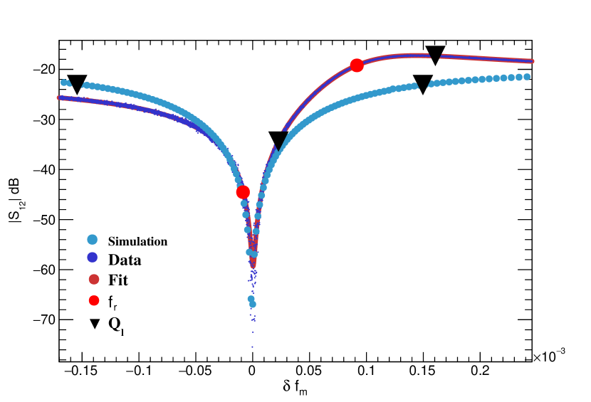
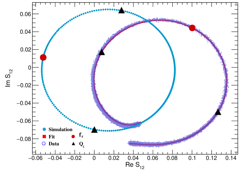
In Fig. 8 we observe that the resonance frequency of the data appears above the baseline and the same for the bandwidth . Due to our resonators have an asymmetry in the transmission amplitude dB, the resonance frequency is not in the minimum and the is not at -3 dB respect to the baseline. In Fig. 9, the is always in the point with maximum phase velocity and the bandwidth divides the circle by the half. Those properties are observed in all the resonators, independently if they are simulated or experimentally measured.
We use TMINUIT with the initial values of all parameters to obtain the resonance frequency and loaded quality factor for each resonator. Next, we define the error of the fit as
| (6) |
In this way, we can establish that two or more resonators are identical if the difference between their resonance frequencies is lower than their maximum .
| MKIDs | ||||||||
|---|---|---|---|---|---|---|---|---|
| A1 | B1 | A2 | B2 | |||||
| Resonator | (GHz) | (GHz) | (GHz) | (GHz) | ||||
| 10 | 1.0697 | 147.6 | 1.0967 | 74.8 | 1.0207 | 103.0 | 1.0376 | 44.7 |
| 1 | 1.1038 | 3.6 | 1.1408 | 10.1 | 1.0645 | 8.0 | 1.0869 | 31.7 |
| 12 | 1.2868 | 31.4 | 1.3148 | 84.8 | 1.2160 | 54.7 | 1.2275 | 155.8 |
| 3 | 1.3136 | 32.2 | 1.3495 | 4.0 | 1.2487 | 8.0 | 1.2813 | 3.2 |
| 7 | 1.5594 | 165.6 | 1.6073 | 61.0 | 1.5113 | 89.4 | 1.5516 | 46.5 |
| 5 | 1.6116 | 8.4 | 1.6532 | 10.0 | 1.5312 | 10.5 | 1.5620 | 3.5 |
| 11 | 1.9603 | 104.3 | 2.0037 | 35.0 | 1.8603 | 95.6 | 1.8872 | 232.6 |
| 2 | 1.9890 | 1.9 | 2.0482 | 16.6 | 1.9212 | 6.5 | 1.9728 | 7.0 |
| 4 | 2.7363 | 54.4 | 2.8119 | 28.0 | 2.6269 | 26.7 | 2.6826 | 70.8 |
| 8 | 2.7868 | 2.0 | 2.8559 | 4.6 | 2.6691 | 6.5 | 2.6996 | 3.5 |
| 9 | 4.2118 | 80.8 | 4.3164 | 125.7 | 4.0898 | 29.1 | 4.1386 | 55.4 |
| 6 | 4.2970 | 31.8 | 4.4136 | 42.0 | 4.1653 | 6.3 | 4.1821 | 4.6 |
Appendix B Critical Temperature
To extract the critical temperature through the fractional change of the resonance frequency we perform a chi-squared fit
| (7) |
where the error is the median absolute deviation (MAD) and is global. The data set of the MAD is obtained from the error propagation of .
| (K) | ||||
|---|---|---|---|---|
| Resonator | A1 | B1 | A2 | B2 |
| 10 | 4.05 | 4.06 | 4.12 | 4.11 |
| 1 | 4.05 | 4.06 | 4.12 | 4.11 |
| 12 | 4.05 | 4.06 | 4.12 | 4.12 |
| 3 | 4.05 | 4.06 | 4.12 | 4.10 |
| 7 | 4.05 | 4.05 | 4.12 | 4.11 |
| 5 | 4.06 | 4.06 | 4.11 | 4.10 |
| 11 | 4.05 | 4.05 | 4.12 | 4.12 |
| 2 | 4.05 | 4.05 | 4.12 | 4.11 |
| 4 | 4.05 | 4.05 | 4.11 | 4.10 |
| 8 | 4.05 | 4.05 | 4.11 | 4.10 |
| 9 | 4.04 | 4.05 | 4.10 | 4.10 |
| 6 | 4.05 | 4.05 | 4.11 | 4.09 |
Appendix C Kinetic Inductance
From equation (1), we can derive the kinetic inductance of a resonator using the values of , and . Depending on the design of the resonators, in some cases it is possible to determine the values of and by analytical methods Anlatyc_Lg . However, in our case, it is complicated due to the complexity of the design.
Running a simulation with different values of , from 15 pH/sq to 40 pH/sq in steps of 2 pH/sq, we obtained as a function of . Then, we did a fit to equation (1) and the values of the geometrical capacitance and geometrical inductance of each resonator were extracted. From the simulation we have identified the 12 resonators and the order in which they appear in the frequency space, which is independent of the value of . This allows us to identify to which resonator corresponds each resonance frequency when we analyze the spectrum of the MKID (see Fig. 4).
Fig. 11 shows a histogram of the local kinetic inductance of the 48 resonators derived from the measured value of and the simulated values of and . We can obtain a unique value of the kinetic inductance of all resonators, referred to as global kinetic inductance , through finding the value of that minimizes the next function
| (8) |
In the equation (8) the sum runs over all 12 resonance frequencies and the error is calculated with equation (6).
Fig. 11 shows the values of the global kinetic inductance derived with the previous methods.

C.1 Citations and References
References
- (1) R. Cristiano, M. Ejrnaes, E. Esposito, M. P Lisitskyi, C. Nappi, S. Pagano, and D. Perez de Lara, Nonequilibrium superconducting detectors, Superconductor Science and Technology 19 (03, 2006) S152.
- (2) W. Guo et al., Counting Near Infrared Photons with Microwave Kinetic Inductance Detectors, Appl. Phys. Lett. 110 (2017) 212601, [arXiv:1702.07993].
- (3) B. A. Mazin, S. R. Meeker, M. J. Strader, P. Szypryt, D. Marsden, J. C. van Eyken, G. E. Duggan, A. B. Walter, G. Ulbricht, M. Johnson, B. Bumble, K. O’Brien, and C. Stoughton, ARCONS: A 2024 Pixel Optical through Near-IR Cryogenic Imaging Spectrophotometer, PASP 125 (Nov., 2013) 1348, [arXiv:1306.4674].
- (4) E. Shirokoff, P. S. Barry, C. M. Bradford, G. Chattopadhyay, P. Day, S. Doyle, S. Hailey-Dunsheath, M. I. Hollister, A. Kovács, C. McKenney, H. G. Leduc, N. Llombart, D. P. Marrone, P. Mauskopf, R. O’Brient, S. Padin, T. Reck, L. J. Swenson, and J. Zmuidzinas, MKID development for SuperSpec: an on-chip, mm-wave, filter-bank spectrometer, in Millimeter, Submillimeter, and Far-Infrared Detectors and Instrumentation for Astronomy VI, vol. 8452 , p. 84520R, Sept., 2012. arXiv:1211.1652.
- (5) M. Faverzani, P. Day, A. Nucciotti, and E. Ferri, Developments of microresonators detectors for neutrino physics in milan, Journal of Low Temperature Physics 167 (Jun, 2012) 1041–1047.
- (6) M. Hofheinz, E. M. Weig, M. Ansmann, R. C. Bialczak, E. Lucero, M. Neeley, A. D. O’Connell, H. Wang, J. M. Martinis, and A. N. Cleland, Generation of fock states in a superconducting quantum circuit, Nature 454 (07, 2008) 310 EP –.
- (7) A. A. Houck, D. I. Schuster, J. M. Gambetta, J. A. Schreier, B. R. Johnson, J. M. Chow, L. Frunzio, J. Majer, M. H. Devoret, S. M. Girvin, and R. J. Schoelkopf, Generating single microwave photons in a circuit, Nature 449 (09, 2007) 328 EP –.
- (8) A. Wallraff, D. I. Schuster, A. Blais, L. Frunzio, R. S. Huang, J. Majer, S. Kumar, S. M. Girvin, and R. J. Schoelkopf, Strong coupling of a single photon to a superconducting qubit using circuit quantum electrodynamics, Nature 431 (09, 2004) 162 EP –.
- (9) R. J. Schoelkopf and S. M. Girvin, Wiring up quantum systems, Nature 451 (02, 2008) 664 EP –.
- (10) S. Golwala, J. Gao, D. Moore, B. Mazin, M. Eckart, B. Bumble, P. Day, H. G. Leduc, and J. Zmuidzinas, A WIMP Dark Matter Detector Using MKIDs, Journal of Low Temperature Physics 151 (Apr., 2008) 550–556.
- (11) P. Szypryt, B. A. Mazin, B. Bumble, H. G. Leduc, and L. Baker, Ultraviolet, Optical, and Near-IR Microwave Kinetic Inductance Detector Materials Developments, IEEE Trans. Appl. Supercond. 25 (2016) 1–4, [arXiv:1412.0724]. [IEEE Trans. Appl. Supercond.25,7598(2015)].
- (12) R. W. Johnson, A. Hultqvist, and S. F. Bent, A brief review of atomic layer deposition: from fundamentals to applications, Materials Today 17 (2014), no. 5 236 – 246.
- (13) W. Spengler, R. Kaiser, A. N. Christensen, and G. Müller-Vogt, Raman scattering, superconductivity, and phonon density of states of stoichiometric and nonstoichiometric tin, Phys. Rev. B 17 (Feb, 1978) 1095–1101.
- (14) W. Tsai, M. Delfino, J. A. Fair, and D. Hodul, Temperature dependence of the electrical resistivity of reactively sputtered tin films, Journal of Applied Physics 73 (1993), no. 9 4462–4467, [https://doi.org/10.1063/1.352785].
- (15) B. Sacépé, C. Chapelier, T. I. Baturina, V. M. Vinokur, M. R. Baklanov, and M. Sanquer, Disorder-induced inhomogeneities of the superconducting state close to the superconductor-insulator transition, Phys. Rev. Lett. 101 (Oct, 2008) 157006.
- (16) L. Toth, C. Wang, and G. Yen, Superconducting critical temperatures of nonstoichiometric transition metal carbides and nitrides, Acta Metallurgica 14 (1966), no. 11 1403 – 1408.
- (17) T. P. Thorpe, S. B. Qadri, S. A. Wolf, and J. H. Claassen, Electrical and optical properties of sputtered tinx films as a function of substrate deposition temperature, Applied Physics Letters 49 (1986), no. 19 1239–1241, [https://doi.org/10.1063/1.97425].
- (18) J. Baselmans, S. Yates, P. de Korte, H. Hoevers, R. Barends, J. Hovenier, J. Gao, and T. Klapwijk, Development of high-q superconducting resonators for use as kinetic inductance detectors, Advances in Space Research 40 (2007), no. 5 708 – 713.
- (19) P. K. Day, H. G. LeDuc, B. A. Mazin, A. Vayonakis, and J. Zmuidzinas, A broadband superconducting detector suitable for use in large arrays, Nature 425 (10, 2003) 817 EP –.
- (20) A. Dominjon, M. Sekine, K. Karatsu, T. Noguchi, Y. Sekimoto, S. Shu, S. Sekiguchi, and T. Nitta, Study of superconducting bilayer for microwave kinetic inductance detectors for astrophysics, IEEE Transactions on Applied Superconductivity 26 (April, 2016) 1–6.
- (21) S. Doyle, Lumped Element Kinetic Inductance Detectors. PhD thesis, Cardiff University, 2008.
- (22) T. Noguchi, A. Dominjon, and Y. Sekimoto, Analysis of Characteristics of Al MKID Resonators, IEEE Transactions on Applied Superconductivity 28 (June, 2018) 2809615, [arXiv:1709.10421].
- (23) J. Gao, J. Zmuidzinas, B. Mazin, P. Day, and H. Leduc, Experimental study of the kinetic inductance fraction of superconducting coplanar waveguide, Nuclear Instruments and Methods in Physics Research Section A: Accelerators, Spectrometers, Detectors and Associated Equipment 559 (2006), no. 2 585 – 587. Proceedings of the 11th International Workshop on Low Temperature Detectors.
- (24) E. F. C. Driessen, P. C. J. J. Coumou, R. R. Tromp, P. J. de Visser, and T. M. Klapwijk, Strongly disordered tin and nbtin -wave superconductors probed by microwave electrodynamics, Phys. Rev. Lett. 109 (Sep, 2012) 107003.
- (25) P. Anderson, Theory of dirty superconductors, Journal of Physics and Chemistry of Solids 11 (1959), no. 1 26 – 30.
- (26) M. S. Khalil, M. J. A. Stoutimore, F. C. Wellstood, and K. D. Osborn, An analysis method for asymmetric resonator transmission applied to superconducting devices, Journal of Applied Physics 111 (2012), no. 5 054510, [https://doi.org/10.1063/1.3692073].
- (27) I. Besedin and A. P. Menushenkov, Quality factor of a transmission line coupled coplanar waveguide resonator, EPJ Quantum Technology 5 (Jan, 2018) 2.
- (28) S. Probst, F. B. Song, P. A. Bushev, A. V. Ustinov, and M. Weides, Efficient and robust analysis of complex scattering data under noise in microwave resonators, Review of Scientific Instruments 86 (Feb, 2015) 024706, [arXiv:1410.3365].
- (29) H. M. I. Jaim, J. A. A. Aguilar, B. Sarabi, Y. J. Rosen, A. N. Ramanayaka, E. H. Lock, C. J. K. Richardson, and K. D. Osborn, Superconducting tin films sputtered over a large range of substrate dc bias, IEEE Transactions on Applied Superconductivity 25 (2015) 1–5.
- (30) H. V. Bui, The Physics of Superconducting Microwave Resonators. PhD thesis, University of Twente, Enschede, the Netherlands, 2013.
- (31) M. R. Vissers, J. Gao, M. Sandberg, S. M. Duff, D. S. Wisbey, K. D. Irwin, and D. P. Pappas, Proximity-coupled ti/tin multilayers for use in kinetic inductance detectors, Applied Physics Letters 102 (2013), no. 23 232603, [https://doi.org/10.1063/1.4804286].
- (32) G. Coiffard, K.-F. Schuster, E. F. C. Driessen, S. Pignard, M. Calvo, A. Catalano, J. Goupy, and A. Monfardini, Uniform Non-stoichiometric Titanium Nitride Thin Films for Improved Kinetic Inductance Detector Arrays, Journal of Low Temperature Physics 184 (Aug., 2016) 654–660, [arXiv:1510.01876].
- (33) C. M. McKenney et al., Tile-and-trim micro-resonator array fabrication optimized for high multiplexing factors, Rev. Sci. Instrum. 90 (2019), no. 2 023908, [arXiv:1803.04275].
- (34) R. Levy, Microelectronic Materials and Processes. Springer Netherlands, 2012.
- (35) P. J. Petersan and S. M. Anlage, Measurement of resonant frequency and quality factor of microwave resonators: Comparison of methods, Journal of Applied Physics 84 (Sept., 1998) 3392–3402, [cond-mat/9805365].
- (36) I. Besedin and A. P. Menushenkov, Quality factor of a transmission line coupled coplanar waveguide resonator, EPJ Quantum Technology 5 (Jan, 2018) 2.