Global optimization of an encapsulated Si/SiO2 L3 cavity for ultra-high quality factor
Abstract
We optimize a silica-encapsulated silicon L3 photonic crystal cavity for ultra-high quality factor by means of a global optimization strategy, where the closest holes surrounding the cavity are varied to minimize out-of-plane losses. We find an optimal value of , thus setting a new record for encapsulated low-index-contrast photonic crystal cavities. We also address the effects of structural imperfections on our optimal cavity design and predict an averaged in the 2 million regime for state-of-the-art silicon fabrication tolerances.
Photonic crystal (PC) slab cavities have been focus of intense research during the last two decades due to their unique properties to efficiently confine light at length scales close to the diffraction limit, and extremely low loss rates Vahala (2003); Akahane et al. (2003). These features have allowed to study a wide variety of classical and quantum phenomena, where the linear and non-linear interactions between light and matter are effectively enhanced in the cavity region Yoshie et al. (2004); Englund et al. (2005); Hennessy et al. (2007); Noda et al. (2007); Faraon et al. (2008); O’Brien et al. (2009); Rivoire et al. (2009); Husko et al. (2009); Nomura et al. (2010); Nozaki et al. (2010); Galli et al. (2010); Ellis et al. (2011); Reinhard et al. (2012); Nozaki et al. (2012); Volz et al. (2012); Shakoor et al. (2013); Takahashi et al. (2013); Dharanipathy et al. (2014). Broadly speaking, the strength of this enhancement grows with the local density of electromagnetic states, which is proportional to the quality factor of the cavity mode , and inversely proportional to its mode volume Yao et al. (2010); Kristensen and Hughes (2014); Vasco and Hughes (2018). Hence, massive efforts have been directed toward the optimization of these figures of merit in order to reach the desired functionality of the photonic device Chalcraft et al. (2007); Minkov and Savona (2014); Tanaka et al. (2008); Minkov et al. (2017); Asano and Noda (2018); Minkov et al. (2019). Particularly, silicon-based cavities have attracted very much attention because of their natural compatibility with CMOS technologies and negligible material losses at telecom wavelengths, allowing the integration with optoelectronic devices in a single chip Wang and Long (2018). While free-standing silicon PC slabs offer an excellent platform to build ultralow loss cavities Asano et al. (2017); Minkov et al. (2017); Simbula et al. (2017), silica (SiO2) encapsulation improves the mechanical stability and thermal dissipation of the system Bazin et al. (2014a), while mitigating additional loss channels coming from the etching of air holes in the silicon Borselli et al. (2006). Nevertheless, high quality factors are challenging in such encapsulated structures given the low refractive index contrast between the two materials.
In this letter, we employ a global optimization approach to maximize the quality factor of a Si/SiO2 L3 PC cavity. We find an optimal quality factor of which corresponds to the largest value achieved for low-index-contrast PC cavities. Our results set a new record for the L3 paradigm and open the way to a new class of highly efficient optical devices for linear and non-linear applications in classical and quantum photonics.
| Si/SiO2 – L3 cavity | (Thz) | |||||
|---|---|---|---|---|---|---|
| Non-optimized | 195.2 | 0.67 | 3.25 | |||
| Optimized | 191.2 | 1.75 | 7.47 |
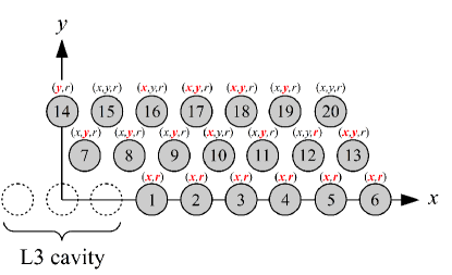
We consider a silica-encapsulated silicon PC slab with a hexagonal lattice of holes of radii nm, lattice parameter nm and thickness nm. A L3 cavity is introduced by removing three holes along the direction of the lattice. In order to optimize the quality factor of its fundamental mode, we adopt a global optimization approach in which only the closest holes surrounding the cavity are varied, in size and position , to reduce out-of-plane losses. This technique has been extremely successful during the last few years to reach record theoretical and experimental quality factors for a wide variety of different materials and cavity geometries Dharanipathy et al. (2014); Minkov and Savona (2014); Lai et al. (2014); Triviño et al. (2014); Flayac et al. (2015); Minkov et al. (2017); Vasco et al. (2019). Specifically, we employ the particles swarm (PS) algorithm to achieve this goal with as the objective function and the guided mode expansion method (GME) Andreani and Gerace (2006) as the main PC solver. We show in Fig. 1 the schematic representation of the holes to be considered in the optimization procedure, where mirror symmetry with respect to the planes and is assumed. Notice that in such a way we end up with a total of 53 optimization parameters, however, after 1400 iterations of the PS algorithm we have noticed that the most relevant parameters for increasing are those highlighted in red in Fig. 1. This preliminary analysis allowed us to reduce the dimension of the optimization parameter space from 53 to 27, thus effectively decreasing the number of function evaluations required by the algorithm to converge. We summarize in Table 1 our final results where
| (1) |
is the linear mode volume and
| (2) |
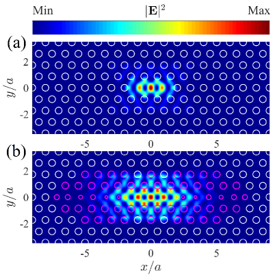
is the non-linear one Barclay et al. (2005), with representing the dielectric function of the system and the electric field of the cavity mode. A global maximum of (computed with FDTD lum ) is found after 806200 function evaluations, leading to an improvement of four orders of magnitude with respect to the non-optimized cavity. This theoretical quality factor is the largest reported for silica-encapsulated PC cavities so far Quan et al. (2010); Bazin et al. (2014b); Vasco et al. (2019), setting a new record for ultra-high cavities in low-index-contrast PCs. It is important to notice that, different from previous optimizations of the L3 cavity Minkov and Savona (2014), is optimized at the expense of the linear and non-linear mode volumes, nevertheless, we still get extremely large enhancement factors and which are in the and regimes, respectively. The increase of the mode volume is clearly seen in the Fig. 2, where we plot the near-field intensity distribution of the fundamental cavity mode in the middle of the slab, for the non-optimized cavity, Fig. 2(a), and the optimized one, Fig. 2(b). The holes which are actually varied are represented by magenta circles in Fig. 2(b). The optimal parameters of the cavity as well as the far-filed projection of the near-field components are reported in the Appendices A and B, respectively.
The same optimization strategy can be directly applied to the air-bridge silicon L3 cavity within the same parameter space of dimension 27. For this configuration, we have obtained an FDTD quality factor which is around 20 times larger than the previous record obtained with deep neural networks Asano and Noda (2019). While our optimization requires a much larger number of evaluations to find the global maximum of the objective function, it clearly shows that there is still considerable room for further improvement of these figures of merit when increasing the size of the optimization parameter space. Detailed results for the Si/Air L3 cavity are given in the Appendix C.
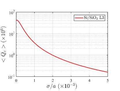
Since any realistic sample is always subject to a small amount of intrinsic disorder, coming from unavoidable imperfections introduced during the fabrication stage, we model such effect by considering random Gaussian fluctuations in all hole positions and sizes of our PC, where the standard deviation of the Gaussian probability distribution is taken as the disorder parameter Gerace and Andreani (2004); Minkov et al. (2013); Vasco and Savona (2018). Results of this analysis are shown in Fig. 3, where the averaged cavity quality factor , computed over 100 independent disorder realization of the system, is plotted as a function of . Typical tolerances in silicon state-of-the-art fabrication techniques range between and Asano et al. (2017); Mohamed et al. (2018), leading to an averaged in the 2 million regime, which still correspond to a record figure of merit for silica encapsulated PC structures.
In conclusion, we have optimized a silica-encapsulated silicon L3 cavity by means of a global optimization strategy, where the closest holes surrounding the cavity are varied to decrease out-of-plane losses. We have found a record value of which is around four times larger than the previous best obtained for Si/SiO2 structures, achieved in nanobeam geometries. To better relate our optimal design to realistic samples, we have also studied the effects of intrinsic disorder and found that when considering typical tolerances in modern fabrication techniques, the averaged quality factor of the optimized cavity remains in the 2 million regime, corresponding to an outstanding result given the low-index contrast of the Si/SiO2 configuration. Apart from setting a new record for the L3 cavity, our results clearly show that there is still a vast room for further improvement of different figures of merit in photonics when increasing the size of the optimization space, and open the way to a new class of optimized designs in low-index-contrast materias, such as AlN, GaN or Si3N4, holding great promise for nonlinear optical enhancement, sensing, and solid-state quantum optics.
Appendix A Optimal parameters of the encapsulated L3 cavity
The optimal 27 parameters of the Si/SiO2 L3 cavity with an FDTD quality factor of are reported in Table 2.
| ParameterHole | 1 | 2 | 3 | 4 | 5 | 6 | 7 | 8 | 9 | 10 |
|---|---|---|---|---|---|---|---|---|---|---|
| 0.4407 | 0.3817 | 0.3936 | 0.3352 | 0.3097 | 0.1385 | 0.0010 | ||||
| 0.0109 | 0.0107 | 0.0082 | ||||||||
| -0.1500 | -0.1500 | -0.0772 | -0.1075 | -0.0690 | -0.0672 | |||||
| ParameterHole | 11 | 12 | 13 | 14 | 15 | 16 | 17 | 18 | 19 | 20 |
| -0.0044 | 0.0010 | 0.0018 | 0.0017 | |||||||
| 0.0027 | 0.0121 | -0.0010 | -0.0044 | -0.0081 | -0.0071 | |||||
| 0.0001 |
Appendix B Fourier transform of near-field components
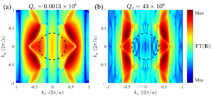
The far-field projections of the mode components for the non-optimized and optimized cavities, are shown in Figs. 4(a) and 4(b), respectively, in log scale. This projection is obtained through the Fourier transform of the near-field components Vučković et al. (2002), recorded in a plane localized at nm above the photonic crystal surface. The dashed circle represents the region where the cavity frequency crosses the light-line. The strong reduction of the field components inside the light cone (or equivalently, above the light-line) is clearly seen for the optimized design.
Appendix C Results for the Si/Air L3 cavity
The Si/Air (air-bridge) L3 cavity is considered in a silicon PC with a hexagonal lattice of holes with radii nm, lattice parameter nm and slab thickness nm. The PS optimization is carried out by considering the same 27 parameters of the Si/SiO2 case.
C.1 Optimal figures of merit
We show in Table 3 the linear and non-linear figures of merit of both, non-optimized and optimized designs. The quality factor is improved by four orders of magnitude with a final FDTD value of , which is around 20 times larger than the previous best, for the silicon L3 cavity, obtained with deep learning optimization techniques Asano and Noda (2019).
| Si/Air – L3 cavity | (Thz) | |||||
|---|---|---|---|---|---|---|
| Non-optimized | 196.3 | 0.59 | 2.48 | |||
| Optimized | 193.6 | 1.07 | 4.30 |
C.2 Optimal parameters
The optimal parameters for the Si/Air L3 cavity with are reported in Table 4
| ParameterHole | 1 | 2 | 3 | 4 | 5 | 6 | 7 | 8 | 9 | 10 |
|---|---|---|---|---|---|---|---|---|---|---|
| 0.3800 | 0.2954 | 0.2000 | 0.4032 | 0.2360 | 0.0475 | -0.0179 | ||||
| -0.0232 | -0.0157 | 0.0028 | ||||||||
| -0.0445 | -0.0174 | 0.0033 | -0.0433 | -0.1500 | -0.0805 | |||||
| ParameterHole | 11 | 12 | 13 | 14 | 15 | 16 | 17 | 18 | 19 | 20 |
| -0.0341 | 0.0040 | -0.0001 | -0.0059 | |||||||
| -0.0600 | -0.0141 | -0.0078 | 0.0083 | -0.0114 | -0.0307 | |||||
| -0.0427 |
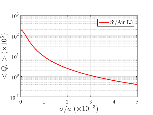
C.3 Disorder analysis
Figure 5 show the disorder analysis for the optimal air-bridge L3 cavity. An averaged in the 4 million regime is predicted for typical tolerances, ranging between and , in silicon fabrication techniques Asano et al. (2017); Mohamed et al. (2018).
References
- Vahala (2003) K. J. Vahala, Nature 424, 839 (2003).
- Akahane et al. (2003) Y. Akahane, T. Asano, B.-S. Song, and S. Noda, Nature 425, 944 (2003).
- Yoshie et al. (2004) T. Yoshie, A. Scherer, J. Hendrickson, G. Khitrova, H. M. Gibbs, G. Rupper, C. Ell, O. B. Shchekin, and D. G. Deppe, Nature 432, 200 (2004).
- Englund et al. (2005) D. Englund, D. Fattal, E. Waks, G. Solomon, B. Zhang, T. Nakaoka, Y. Arakawa, Y. Yamamoto, and J. Vučković, Phys. Rev. Lett. 95, 013904 (2005).
- Hennessy et al. (2007) K. Hennessy, A. Badolato, M. Winger, D. Gerace, M. Atatüre, S. Gulde, S. Fält, E. L. Hu, and A. Imamoğlu, Nature 445, 896 (2007).
- Noda et al. (2007) S. Noda, M. Fujita, and T. Asano, Nat. Photonics 1, 449 (2007).
- Faraon et al. (2008) A. Faraon, I. Fushman, D. Englund, N. Stoltz, P. Petroff, and J. Vučković, Nat. Phys. 4, 859 (2008).
- O’Brien et al. (2009) J. L. O’Brien, A. Furusawa, and J. Vučković, Nat. Photonics 3, 687 (2009).
- Rivoire et al. (2009) K. Rivoire, Z. Lin, F. Hatami, W. T. Masselink, and J. Vučković, Opt. Express 17, 22609 (2009).
- Husko et al. (2009) C. Husko, A. D. Rossi, S. Combrié, Q. V. Tran, F. Raineri, and C. W. Wong, Appl. Phys. Lett. 94, 021111 (2009).
- Nomura et al. (2010) M. Nomura, N. Kumagai, S. Iwamoto, Y. Ota, and Y. Arakawa, Nat. Phys. 6, 279 (2010).
- Nozaki et al. (2010) K. Nozaki, T. Tanabe, A. Shinya, S. Matsuo, T. Sato, H. Taniyama, and M. Notomi, Nat. Photonics 4, 477 (2010).
- Galli et al. (2010) M. Galli, D. Gerace, K. Welna, T. F. Krauss, L. O’Faolain, G. Guizzetti, and L. C. Andreani, Opt. Express 25, 26613 (2010).
- Ellis et al. (2011) B. Ellis, M. A. Mayer, G. Shambat, T. Sarmiento, J. Harris, E. E. Haller, and J. Vučković, Nat. Photonics 5, 297 (2011).
- Reinhard et al. (2012) A. Reinhard, T. Volz, M. Winger, A. Badolato, K. J. Hennessy, E. L. Hu, and A. Imamoğlu, Nat. Photonics 6, 93 (2012).
- Nozaki et al. (2012) K. Nozaki, A. Shinya, S. Matsuo, Y. Suzaki, T. Segawa, T. Sato, Y. Kawaguchi, R. Takahashi, and M. Notomi, Nat. Photonics 6, 248 (2012).
- Volz et al. (2012) T. Volz, A. Reinhard, M. Winger, A. Badolato, K. J. Hennessy, E. L. Hu, and A. Imamoğlu, Nat. Photonics 6, 605 (2012).
- Shakoor et al. (2013) A. Shakoor, R. L. Savio, P. Cardile, S. L. Portalupi, D. Gerace, K. Welna, S. Boninelli, G. Franzò, F. Priolo, T. F. Krauss, M. Galli, and L. O’Faolain, Laser Photonics Rev. 7, 114 (2013).
- Takahashi et al. (2013) Y. Takahashi, Y. Inui, M. Chihara, T. Asano, R. Terawaki, and S. Noda, Nature 498, 470 (2013).
- Dharanipathy et al. (2014) U. P. Dharanipathy, M. Minkov, M. Tonin, V. Savona, and R. Houdré, Appl. Phys. Lett. 105, 101101 (2014).
- Yao et al. (2010) P. Yao, V. M. Rao, and S. Hughes, Laser Photonics Rev. 4, 499 (2010).
- Kristensen and Hughes (2014) P. T. Kristensen and S. Hughes, ACS Photonics 1, 2 (2014).
- Vasco and Hughes (2018) J. Vasco and S. Hughes, ACS Photonics 5, 1262 (2018).
- Chalcraft et al. (2007) A. R. A. Chalcraft, S. Lam, D. O’Brien, T. F. Krauss, M. Sahin, D. Szymanski, D. Sanvitto, R. Oulton, M. S. Skolnick, A. M. Fox, D. M. Whittaker, H.-Y. Liu, and M. Hopkinson, Appl. Phys. Lett. 90, 241117 (2007).
- Minkov and Savona (2014) M. Minkov and V. Savona, Sci. Rep. 4, 5124 (2014).
- Tanaka et al. (2008) Y. Tanaka, T. Asano, and S. Noda, J. Light. Technol 26, 1532 (2008).
- Minkov et al. (2017) M. Minkov, V. Savona, and D. Gerace, Appl. Phys. Lett. 111, 131104 (2017).
- Asano and Noda (2018) T. Asano and S. Noda, Opt. Express 26, 32704 (2018).
- Minkov et al. (2019) M. Minkov, D. Gerace, and S. Fan, Optica 6, 1039 (2019).
- Wang and Long (2018) J. Wang and Y. Long, Sci. Bull. 63, 1267 (2018).
- Asano et al. (2017) T. Asano, Y. Ochi, Y. Takahashi, K. Kishimoto, and S. Noda, Opt. Express 25, 1769 (2017).
- Simbula et al. (2017) A. Simbula, M. Schatzl, L. Zagaglia, F. Alpeggiani, L. C. Andreani, F. Schäffler, T. Fromherz, M. Galli, and D. Gerace, APL photonics 2, 056102 (2017).
- Bazin et al. (2014a) A. Bazin, P. Monnier, X. Lafosse, G. Beaudoin, R. Braive, I. Sagnes, R. Raj, and F. Raineri, Opt. Express 22, 10570 (2014a).
- Borselli et al. (2006) M. Borselli, T. J. Johnson, and O. Painter, Appl. Phys. Lett. 88, 131114 (2006).
- Lai et al. (2014) Y. Lai, S. Pirotta, G. Urbinati, D. Gerace, M. Minkov, V. Savona, A. Badolato, and M. Galli, Appl. Phys. Lett. 104, 241101 (2014).
- Triviño et al. (2014) N. V. Triviño, M. Minkov, G. Urbinati, M. Galli, J.-F. Carlin, R. Butté, V. Savona, and N. Grandjean, Appl. Phys. Lett. 105, 231119 (2014).
- Flayac et al. (2015) H. Flayac, M. Minkov, and V. Savona, Phys. Rev. A 92, 043812 (2015).
- Vasco et al. (2019) J. Vasco, D. Gerace, and V. Savona, arXiv:1910.10647 (2019).
- Andreani and Gerace (2006) L. C. Andreani and D. Gerace, Phys. Rev. B 73, 235114 (2006).
- Barclay et al. (2005) P. E. Barclay, S. Kartik, and O. Painter, Opt. Express 13, 801 (2005).
- (41) Lumerical Solutions, Inc. , https://www.lumerical.com/tcad.
- Quan et al. (2010) Q. Quan, P. B. Deotare, and M. Loncar, Appl. Phys. Lett. 96, 203102 (2010).
- Bazin et al. (2014b) A. Bazin, R. Raj, and F. Raineri, J. Light. Technol 32, 952 (2014b).
- Asano and Noda (2019) T. Asano and S. Noda, arXiv:1908.03702 (2019).
- Gerace and Andreani (2004) D. Gerace and L. C. Andreani, Opt. Lett. 29, 1897 (2004).
- Minkov et al. (2013) M. Minkov, U. P. Dharanipathy, R. Houdré, and V. Savona, Opt. Express 21, 28233 (2013).
- Vasco and Savona (2018) J. Vasco and V. Savona, New J. Phys. 20, 075002 (2018).
- Mohamed et al. (2018) M. S. Mohamed, Y. Lai, M. Minkov, V. Savona, A. Badolato, and R. Houdré, ACS Photonics 5, 4846 (2018).
- Vučković et al. (2002) J. Vučković, M. Loncar, H. Mabuchi, and A. Scherer, IEEE J. Quantum Electron. 38, 850 (2002).