On the possibility of a terahertz light emitting diode based on a dressed quantum well
Abstract
We consider theoretically the realization of a tunable terahertz light emitting diode from a quantum well with dressed electrons placed in a highly doped p-n junction. In the considered system the strong resonant dressing field forms dynamic Stark gaps in the valence and conduction bands and the electric field inside the p-n junction makes the QW asymmetric. It is shown that the electrons transiting through the light induced Stark gaps in the conduction band emit photons with energy directly proportional to the dressing field. This scheme is tunable, compact, and shows a fair efficiency.
I Introduction
Terahertz radiation has widespread applications spanning the fields of (astro)physics, biology, medicine, and security Tonouchi_2007 . While semiconductors typically feature in the most compact optoelectronic systems, they are challenging to employ in the terahertz range at which electromagnetic transitions are usually absent. Exceptions have appeared in the use of transitions between exciton-polariton branches ISavenko_2011 ; Barachati_2015 ; Huppert_2014 , direct-indirect exciton transitions Kyriienko_2013 ; Kristinsson_2013 , and interband subband transitions Nathan_2014 , however, potential competition with larger quantum cascade lasers is undemonstrated. Cascade systems based on exciton-polaritons Liew_2013 and nanoparticles Arnardottir_2018 were considered theoretically, but only operate at a fixed frequency. Ideally, a compact semiconductor system could be controlled by an external field to vary its operation frequency.
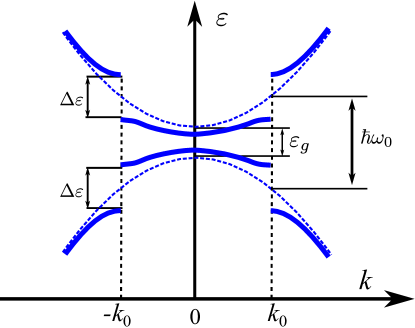
An intense enough electromagnetic field gives rise to a coupled light-matter object known as a dressed electron, which has been studied in various low dimensional systems, including: semiconductor quantum dots Koppenhofer_2016 ; Chestnov_2017 , quantum rings Kozin_2018 ; Sigurdsson_14 , quantum wells Wagner_10 ; Kibis_2012 ; Teich_13 etc. The appearance of band gaps due to the ac Stark effect in the band structure of various nanostructures was first predicted theoretically Goreslavskii_1969 and later observed experimentally Vu_2004 . The strong electromagnetic field mixes the valence and conduction bands of the system and consequently band gaps , tunable in-situ by changing the intensity of the field, appear at the resonant points. In Figure 1 a schematic diagram of the dynamic Stark gaps is shown.
It was previously shown that the dynamic Stark gaps in a quantum well with dressed electrons (dressed QW) can restrict the electron oscillation, which can be used to realize a frequency comb when excited with sub-THz frequency Mandal_2018 . As the frequency of a dynamic Stark gap can be tuned into the THz range, it is natural to ask whether it can serve in the generation of THz radiation. This is far from obvious as in a normal QW electromagnetic transitions across a dynamic Stark gap are forbidden as there is no change in the symmetry between electrons in the states at the top and bottom of the gap Liberato_2013 ; Chestnov_2017 . However, as we will show, the use of an asymmetric QW alleviates this problem. Furthermore, by considering a geometry where the QW is placed between p and n doped semiconductors, we predict that it is possible to realize a pn junction Ando_1982 ; Nag_2000 operating at terahertz frequency. By considering the band-bending diagram and the transition matrix elements in the QW, we determine the relevant transition rates, and employ a simplified rate equation model to estimate the terahertz generation efficiency.
II Band bending of a quantum well in a pn junction
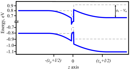
Let us consider an intrinsic QW sandwiched between a p-n junction having doping concentrations and in the p and n sides, respectively. Following Ref. Zeghbroeck_book4 ; Supp_mater the potential variation for the electrons throughout the double heterojunction can be expressed as
| (1) |
Here is the electronic charge; is the permittivity of the material; and are the widths of the depletion regions in the p and n side, respectively; is the thickness of the QW; and are the number of holes and electrons per unit area inside the QW; , is the potential difference between the p side and the n side; is the total built in potential; , , and are the built in potentials in the p side, in the QW, and in the n side, respectively and is the externally applied voltage. The electron and hole density in the QW can be expressed as
| (2) |
Here and are the effective electron and hole masses in the QW. is Boltzmann’s constant and is the temperature. and correspond to the minima and maxima of first electron and hole subbands of the QW, respectively. and are the quasi Fermi levels in the conduction band and in the valence band of the QW, respectively, which can be expressed as joyce_dixon_1977 ; Zeghbroeck_book2
| (3) | ||||
| (4) |
Here is the effective density of states at the conduction band edge of the n type semiconductor; is the effective density of states at the valence band edge of the p type semiconductor; is the minimum of the conduction band in the n side; is the maximum of the valence band in the p side. Using Eqs. (II-4) the quasi Fermi levels of the QW can be controlled. The effect of on the electron and hole potentials throughout the double heterojunction is plotted in Figure 2 where we consider GaAs and AlGaAs as appropriate materials.
III QW energy spectrum under electromagnetic dressing
We consider now that the system is subjected to a linearly polarized high frequency monochromatic electromagnetic field, , which is linearly polarized along the direction (direction perpendicular to the QW plane) with the electric field amplitude and the frequency . For simplicity, we have assumed that the electric field is spatially homogeneous. Assuming that the photon energy is greater than the light-matter interaction characteristic energy (, where d is the interband dipole moment), the corresponding Hamiltonian can be expressed asKibis_2012 ; Janes_Cummings ; Shammah_2015
| (5) |
The superscripts and correspond respectively to the conduction and valence bands; and are photon creation and annihilation operators; and are the electron interband transition operators.
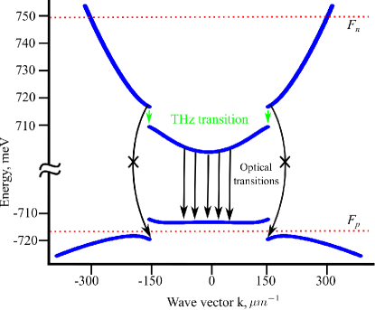
We choose the dressing field frequency such that , where is the band gap of the QW. Under this condition the dressing field strongly mixes the valence band and the conduction band of the quantum well and the stationary state of the system shows energy gaps at the resonant points of the Brillouin zone, , where the energy of the photons matches with the energy difference between the bands (see Figure 1(a)) Goreslavskii_1969 . The modified energy spectrum that arises due to the mixing of the two bands and is expressed by Kibis_2012
| (6) |
Here is the in plane electron wave vector; is the first electron sub-band; is the first hole sub-band; is the resonance detuning; is the dynamic Stark gap. It should be noted that the dressing field amplitude is chosen in such a way that it satisfies the strong light-matter coupling condition and consequently is not absorbed. This condition can be expressed as , where is the Rabi frequency of interband electron transitions and is the average lifetime of the electron states.
IV THz transition matrix element and transition rate
In order to estimate the THz rate we calculate the matrix element for the THz transition, defined as
| (7) |
Here is the wave vector of the emitted photon, and are the dressed conduction and valence band states with photon number , respectively and expressed as Kibis_2012
| (8) | ||||
| (9) |
Here and are the bare conduction and valence band states, respectively; and . In a QW, the wave functions of the conduction and valence sub-bands can be written as
| (10) | |||
| (11) |
where and are the Bloch functions of conduction and valence bands in a bulk semiconductor material; and are the envelope wave functions of the first conduction and valence sub-band arising from the quantization of transverse motion of electrons and holes in the QW. We have to take into account that the Bloch functions, , oscillate with the crystal lattice period, , whereas the characteristic scale of the wave functions is the QW thickness, . Taking the above mentioned conditions into account the interband dipole moment can be expressed as
| (12) |
Since the dipole operator will only act on the electronic part of the wave function and the photon states corresponding to different photon number are orthogonal, the THz matrix element in Eq. (7) can be approximated to
| (13) |
This corresponds to the emitted photons having linear polarization along axis. The matrix elements corresponding to photons having polarization in the other two directions (i.e. along and ) vanish. For a symmetric QW both the terms in Eq. (13) will go to zero separately, but for an asymmetric QW the wave functions and do not have a definite parity resulting in nonzero . Using our parameters we have found that nm which is similar to the one obtained in Ref. Nathan_2014 . The THz transition rate can be expressed as
| (14) |
Here, is the dielectric constant of the QW, is the free space permittivity, is the velocity of light in free space, and is the total number of electronic states in the upper conduction band participating in the THz transition with frequency . In order to realize a monolithic THz source we consider placing the system inside a THz cavity. It is possible to use metal microcavities where the light is confined at sub-wavelength scales in the THz frequency range and the dispersion of the THz photons can be flat Todorov_2010 . This also allows us to neglect THz transitions other than the one that is resonant with the cavity. The presence of the cavity modifies the three dimensional continuum of photonic modes to a two dimensional continuum of photonic modes and Eq. (14) becomes Kakazu_1994
| (15) |
Here is the length of the cavity. Due to the presence of , we choose to calculate numerically using,
| (16) |
where the summation runs over all the initial states . Each electron making the THz transition can also undergo an optical transition directly to the lowest valence band as shown with the dashed arrows in Figure 3. This undesired transition can be stopped by setting at the Stark gap (see Figure 3). It should be noted that the transition from the top conduction band to the top valence band is restricted by momentum conservation. In order to estimate the efficiency of the device we solve the rate equations for different energy bands coupled with the THz photons inside the cavity,
| (17) |
where and are the number of the electrons in the upper and lower conduction band of the QW, respectively; and are the number of THz photons inside the cavity and their lifetime, respectively; is the radiative recombination rate in usual QWs, which has the typical value cm3/s Ridley_1990 ; is the volume of the QW; is the number of holes in the QW, which is calculated from ; is the average lifetime of the electrons, which we take as ns; is the rate at which the electrons are injected into the QW. In principle, the THz transitions corresponding to can be considered, which requires the probability of occupation for each state in the conduction band, however this is beyond the scope of the present work. We limit ourselves to the THz transitions between the states that lie near the Stark gap such that . This allows us to assume that, due to the fast relaxation of the electrons, the lower energy states in the upper conduction band are filled and the higher energy states in the lower conduction band are empty. Electron-electron scattering is likely to increase with the increase in temperature, which will put the system out of the strong coupling regime. To discard any temperature effect we consider that the system is in a low temperature environment such that , which can be achieved using liquid 4He. The input intensity () is defined as
| (18) |
Here , and the first and second term in the right-hand side of Eq. (18) represent the intensity due to the electric current in the device and the dressing field intensity, respectively. The output intensity () is defined as
| (19) |
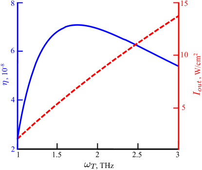
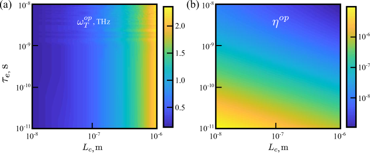
where, the term represents the rate of emission of the THz photons from the cavity. In a GaAs based QW the interband dipole moment, D, and a Stark gap of meV order corresponds to V/cm Goreslavskii_1969 . The efficiency of the device, defined as, , is calculated by finding the steady state of the rate equations in Eq. (IV), which is obtained in a self consistent way where for each THz frequency the total number of electrons in the QW (defined by the ) is kept constant by varying . In Figure 4 the efficiency and output intensity are plotted as a function of THz frequency. The efficiency shows a maximum near 1.5 THz. This corresponds to the Pauli exclusion principle. Once all the electronic states in the lower conduction band are filled the population of the THz photons does not increase even after increasing . Although increases linearly as a function of , increases quadratically resulting in a maximum in the efficiency. It should be noted that can be easily tuned by changing the intensity of the dressing field. As shown in Figure 5, the optimum frequency, , of the THz emission can be controlled mainly by varying with having very little effect on it. However, the optimum efficiency, , decreases with the increase of and . This is understandable, as from Eq. 15 it is clear that THz transition rate, , decreases with the increase of . On the other hand, the average electronic lifetime, , vary depending upon all the possible non-radiative scattering processes. Smaller creates vacancy in the lower conduction band increasing the THz transition probability, which results in higher . The typical efficiency of the device, , which is comparable to other state-of-the-art proposals for THz emission from Stark split bands Nathan_2014 . The main energy cost in the considered system derives from the second term in Eq. (18) (right-hand side), that is, the energy needed to supply the dressing field. As this energy is not absorbed by the system, one could consider that this component of the input energy can be recycled in principle. In such an idealistic case, the efficiency would become . One can also define the quantum efficiency, , which represents the number of THz photons emitted per injected electron. The typical quantum efficiency of the device, , which is very close to unity.
V Conclusion
To conclude, we have considered theoretically a THz source based on a dressed QW inside a highly doped p-n junction coupled to a THz cavity. By solving the rate equations we showed that the system subjected to a forward bias voltage can act as a THz emitting diode having energy efficiency of and quantum efficiency of 0.5. The advantages of our scheme is that it is composed of only one quantum well, making it more compact and easier to fabricate, and the device is tuneable such that it can give different THz frequencies.
VI Acknowledgments
S.M., K.D. and T.L. were supported by the Ministry of Education (Singapore), grant 2017-T2-1-001. O.K. was supported by the Russian Foundation for Basic Research (project 17-02-00053) and Ministry of Science and High Education of Russian Federation (projects 3.4573.2017/6.7 and 3.8051.2017/8.9)
References
- (1) M. Tonouchi, “Cutting-edge terahertz technology”, Nat. Photonics 1, 97 (2007).
- (2) I. G. Savenko, I. A. Shelykh, and M. A. Kaliteevski, “Nonlinear Terahertz Emission in Semiconductor Microcavities”, Phys. Rev. Lett. 107 , 027401 (2011).
- (3) F. Barachati, S. D. Liberato, and S. K. Cohen, “Generation of Rabi-frequency radiation using exciton-polaritons”, Phys. Rev. A 92, 033828 (2015).
- (4) S. Huppert, O. Lafont, E. Baudin, J. Tignon, and R. Ferreira,“Terahertz emission from multiple-microcavity exciton-polariton lasers”, Phys. Rev. B 90, 241302(R) (2014).
- (5) O. Kyriienko, A. V. Kavokin, and I. A. Shelykh, “Superradiant Terahertz Emission by Dipolaritons”, Phys. Rev. Lett. 111, 176401 (2013).
- (6) K. Kristinsson, O. Kyriienko, T. C. H. Liew, and I. A. Shelykh, “Continuous terahertz emission from dipolaritons”, Phys. Rev. B 88, 245303 (2013).
- (7) N. Shammah, C. C. Phillips, and S. D. Liberato, “Terahertz emission from ac Stark-split asymmetric intersubband transitions”, Phys. Rev. B 89, 235309 (2014).
- (8) T. C. H. Liew, M. M. Glazov, K. V. Kavokin, I. A. Shelykh, M. A. Kaliteevski, and A. V. Kavokin, “Proposal for a Bosonic Cascade Laser”, Phys. Rev. Lett. 110, 047402 (2013).
- (9) K. B. Arnardottir and T. C. H. Liew, “Terahertz cascades from nanoparticles”, Phys. Rev. B 97, 195446 (2018).
- (10) M. Koppenhofer and M. Marthaler, “Creation of a squeezed photon distribution using artificial atoms with broken inversion symmetry”, Phys. Rev. A 93, 023831 (2016).
- (11) I. Y. Chestnov, V. A. Shahnazaryan, A. P. Alodjants, I. A. Shelykh, “Terahertz Lasing in Ensemble of Asymmetric Quantum Dots”, ACS Photonics 4, 2726 (2017).
- (12) V. K. Kozin, I. V. Iorsh, O. V. Kibis, and I. A. Shelykh, “Periodic array of quantum rings strongly coupled to circularly polarized light as a topological insulator”, Phys. Rev. B 97, 035416 (2018).
- (13) H. Sigurdsson, O. V. Kibis, and I. A. Shelykh, “Optically induced Aharonov-Bohm effect in mesoscopic rings”, Phys. Rev. B 90, 235413 (2014).
- (14) M. Wagner, H. Schneider, D. Stehr, S. Winner, A. M. Andrews, S. Schartner, G. Strasser, and M. Helm, “Observation of the Intraexciton Autler-Townes Effect in GaAs/AlGaAs Semiconductor Quantum Wells”, Phys. Rev. Lett. 105, 167401 (2010).
- (15) O. V. Kibis, “Persistent current induced by quantum light”, Phys. Rev. B 86, 155108 (2012).
- (16) M. Teich, M. Wagner, H. Schneider, and M. Helm, “Semiconductor quantum well excitons in strong, narrowband terahertz fields”, New J. Phys. 15, 065007 (2013).
- (17) S. P. Goreslavskii and V. F. Elesin, “Electronic properties of a semiconductor in the field of a strong electromagnetic field”, JETP Lett. 10, 316 (1969).
- (18) Q. T. Vu, H. Haug, O. D. Mücke, T. Tritschler, M. Wegener, G. Khitrova, H. M. Gibbs, “Light-Induced Gaps in Semiconductor Band-to-Band Transitions”, Phys. Rev. Lett. 92, 217403 (2004).
- (19) S. Mandal, T. C. H. Liew, and O. V. Kibis, “Semiconductor quantum well irradiated by a two-mode electromagnetic field as a terahertz emitter”, Phys. Rev. A 97, 043860 (2018).
- (20) S. D. Liberato, C. Ciuti, and C. C. Phillips, “Terahertz lasing from intersubband polariton-polariton scattering in asymmetric quantum wells”, Phys. Rev. B 87, 241304(R) (2013).
- (21) B. R. Nag, Physics of Quantum Well Devices, (Klewer, New York, 2000).
- (22) T. Ando, A. B. Fowler, and F. Stern, “Electronic properties of two-dimensional systems”, Rev. Mod. Phys. 54, 437 (1982).
- (23) B. van Zeghbroeck, Principles of Semiconductor Devices and Heterojunctions, Eq. 4.3.9, (Prentice-Hall, Upper Saddle River, 2010).
- (24) See Supplementary Information for the derivation of Eq. (1).
- (25) B. van Zeghbroeck, Principles of Semiconductor Devices and Heterojunctions, Eq. 2.6.19, (Prentice-Hall, Upper Saddle River, 2010).
- (26) W. B. Joyce and R. W. Dixon, “Analytic approximations for the Fermi energy of an ideal Fermi gas”, Appl. Phys. Lett. 31, 354 (1977).
- (27) E.T. Jaynes, F.W. Cummings, “Comparison of quantum and semiclassical radiation theories with application to the beam maser”, Proc. IEEE, 51, 89, 1963.
- (28) N. Shammah and S. D. Liberato, “Theory of intersubband resonance fluorescence”, Phys. Rev. B 92, 201402(R) (2015).
- (29) Y. Todorov, L. Tosetto, J. Teissier, A. M. Andrews, P. Klang, R. Colombelli, I. Sagnes, G. Strasser, and C. Sirtori, “Optical properties of metal-dielectric-metal microcavities in the THz frequency range”, Opt. Express 18, 13886 (2010).
- (30) K. Kakazu and Y. S. Kim, “Quantization of electromagnetic fields in cavities and spontaneous emission”, Phys. Rev. A 50, 1830 (1994).
- (31) B. K. Ridley, “Kinetics of radiative recombination in quantum wells”, Phys. Rev. B 41, 12190 (1990).