Microscopic charging and in-gap states in superconducting granular aluminum
Abstract
Following the emergence of superconducting granular aluminum (grAl) Cohen & Abeles (1968); Deutscher et al. (1973) as a material for high-impedance quantum circuits Grünhaupt et al. (2019); Valenti et al. (2019); Hazard et al. (2019); Zhang et al. (2019), future development hinges on a microscopic understanding of its phase diagram Deutscher et al. (1973); Pracht et al. (2016); Levy-Bertrand et al. (2019), and whether the superconductor-to-insulator transition (SIT) is driven by disorder Anderson (1958); Sacépé et al. (2008, 2011); Driessen et al. (2012); Mondal et al. (2011) or charging effects Mott (1968); Dynes et al. (1984); Bachar et al. (2013, 2015); Moshe et al. (2019). Beyond fundamental relevance, these mechanisms govern noise and dissipation in microwave circuits Feigel’man & Ioffe (2018); Kuzmin et al. (2019). Although the enhancement of the critical temperature, and the SIT in granular superconductors have been studied for more than fifty years Beloborodov et al. (2007), experimental studies have so far provided incomplete information on the microscopic phenomena. Here we present scanning tunneling microscope measurements of the local electronic structure of superconducting grAl. We confirm an increased superconducting gap in individual grains both near and above the Mott resistivity Dynes & Garno (1981); Dynes et al. (1984). Above we find Coulomb charging effects, a first indication for decoupling, and in-gap states on individual grains, which could contribute to flux noise and dielectric loss in quantum devices. We also observe multiple low-energy states outside the gap, which may indicate bosonic excitations of the superconducting order parameter Sherman et al. (2015); Nakamura et al. (2019).
Superconducting granular metals are interesting from a fundamental point of view, because their micro-structure can be seen as a network of artificial atoms coupled by electron tunneling, giving rise to rich physical phenomena Beloborodov et al. (2007). Beyond this fundamental interest, they are also valuable from a quantum circuit engineering perspective thanks to their large kinetic inductance, low microwave frequency losses Grünhaupt et al. (2019); Valenti et al. (2019); Zhang et al. (2019) and amenable non-linearity Maleeva et al. (2018). Granular aluminum (grAl) is particularly appealing due to its ease of fabrication and compatibility with standard Al/AlOx/Al Josephson junction technology. Tuning the oxygen partial pressure during aluminum deposition results in a granular structure, film resistivities from , and consequently variable inter-grain coupling. As a function of , the critical temperature of grAl increases compared to pure aluminum Cohen & Abeles (1968), reaching a maximum in the vicinity of the Mott resistivity Dynes & Garno (1981); Dynes et al. (1984), after which it decreases, and the system becomes insulating at .
Although grAl has been successfully employed in fluxonium quantum bits Grünhaupt et al. (2019), the realization of superconducting quantum processors requires orders of magnitude improvement in coherence. This task is complicated by the fact that several types of imperfections, both microscopic and macroscopic, are concomitantly present, depending on system design, micro-fabrication technology, and materials Krantz et al. (2019). So far, microscopic defects have been measured rather indirectly, through their interaction with the device itself Grabovskij et al. (2012); Wang et al. (2014). It is therefore clear that a local probe, such as scanning tunneling microscopy (STM), can offer precious complementary information about the nature of the observed defects, be that localized spins, charge states, or other microscopic systems.
Charging effects due to grain decoupling have been proposed to govern the SIT in grAl, supported by evidence from tunnel junction spectroscopy, magnetoresistance measurements, and muon spin relaxation Bachar et al. (2015, 2018). Here, we employ the imaging abilities of a 30 mK STM, capable of high energy-resolution spectroscopy Balashov et al. (2018), to resolve localized charge states and to test the presence of both in-gap states and low energy excitations outside the gap.
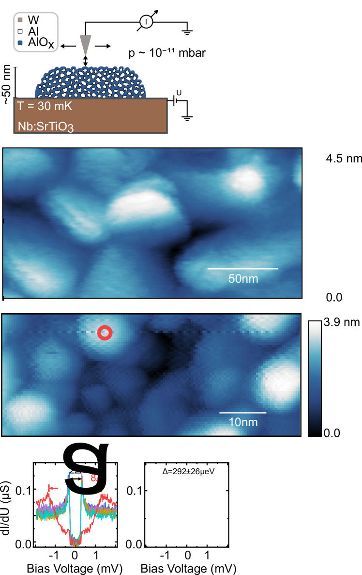
The measurement geometry of the experiment is sketched in Fig. 1a. A conducting Nb doped SrTiO3 (Nb:STO) single crystal substrate is used to apply the sample bias to the film, and the STM tip is scanned over its surface. For topographic images, the bias voltage is selected to be much above the superconducting gap and the STM is operated in the constant current mode, in which the tip is regulated in the z-direction by a feed-back loop such that the tunneling current at the chosen bias voltage is constant. To obtain information on the superconducting gap, the feed-back loop is opened, the position of the tip is fixed and the bias voltage is ramped, while the differential conductivity is measured.
As a control experiment, we start by measuring a thick pure Al film. Figure 1b shows a typical STM image of the film, which consists of crystallites of about 50 nm lateral size. The large size of the crystallites is due to the high diffusion mobility of Al, according to its relatively low melting point. Figure 1c shows the superconducting gap and the coherence peaks in the Al spectrum. The superconducting gap of about , obtained by a fit to the BCS density of states (DOS), is close to the known values for thin-film Al Douglass & Meservey (1964). In all respects, the pure Al sample behaves as expected.
In contrast, Fig. 1d shows a typical topographic image of the sample surface of a grAl film with , i.e., close to the Mott resistivity and the maximum K of the superconducting dome Levy-Bertrand et al. (2019). Superconducting grAl can be viewed as a connected 3D network of Al grains, separated by amorphous AlOx oxide (for film deposition details see Methods). As evident from Fig. 1d, the Al grains in grAl are much smaller compared to the pure Al film, as expected Deutscher et al. (1973). Note that the STM tip, etched from a W wire, cannot be made to arbitrary sharpness, and has a typical radius of curvature in the tens of nm range. Since the topographic image reflects a convolution of the grains and the tip shape, the grains may appear slightly larger in STM images. The observed distribution of grain sizes , however, agrees with the reported values and spread in the literature for similar film growth conditions Deutscher et al. (1973).
Figure 1e shows a selection of differential conductance spectra recorded on different grains. They show a practically identical superconducting gap , yielding a value for the grAl superconducting gap obtained with a BCS fit (see Fig. 1f). Note that this value is significantly larger than that of pure Al (cf. Fig. 1c). For similar grAl films, radio-frequency measurements Valenti et al. (2019) revealed a bulk value for of approximately , extracted from the measurement of the critical temperature , while direct THz spectroscopy Levy-Bertrand et al. (2019) revealed a value of . The surprisingly small difference between these values, obtained using very different methodologies, indicates that grains residing at the surface have a superconducting gap comparable to the bulk of the grAl sample. Additionally, from the fact that all measured grains show the same , we conclude that either the gap enhancement mechanism is homogeneous and robust to variations in grain size, or the grains are coupled strongly enough to even out variations.
On a larger energy scale (see Fig. 1g) the grains show a metallic behaviour, i.e. a DOS that has no conventional band gap. However, the spectra are quantitatively different from grain to grain. The fact that we do not observe a common DOS over several grains indicates that the electron wave functions are not entirely delocalized and electrons are partly reflected at the boundaries, which is expected considering the grains are oriented randomly and are separated by amorphous AlOx barriers.
Note that occasionally, individual grains show a deviating behaviour, as indicated by the red circle in Fig. 1d and the corresponding red spectrum in Fig. 1e. The low energy spectrum of the grain shows reduced coherence peaks, and a secondary gap of approximately . These are the first indications of what will be observed in grAl films with a higher oxygen concentration.
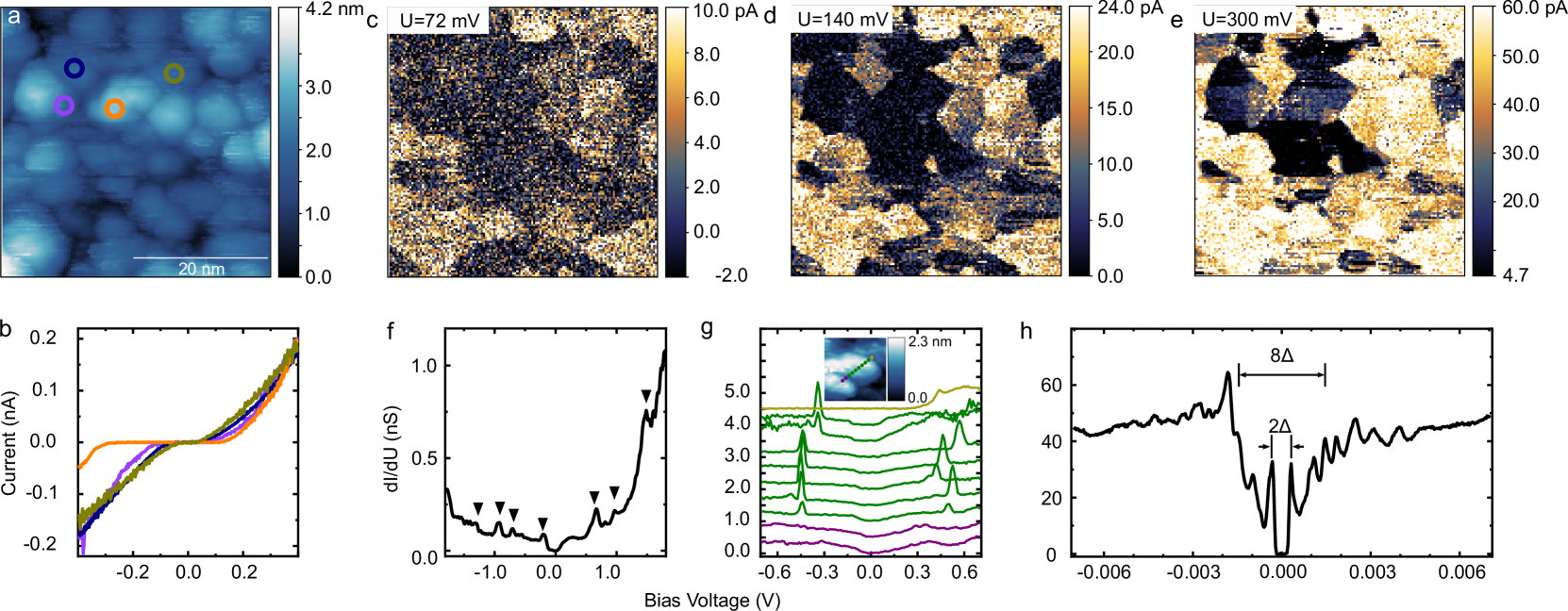
In Fig. 2, we summarize the behaviour of grains in oxygen rich films (). In topography (see Fig. 2a) we observe grains of similar size compared to the oxygen poor films. We also notice sudden jumps in the z-position when scanning some of the grains. These indicate charging effects, as also observed on a few, more insulated grains in Fig. 1d. From the large range measurements shown in Fig. 2b, taken on the individual grains highlighted in Fig. 2a, it becomes obvious that the grains do not entirely behave metallic, but only show large currents above (or below) a certain threshold voltage. The curves also vary from grain to grain. In Fig. 2, panels c-e, we plot measured maps of the tunnel current at several bias voltages (, , and ). Multiple neighbouring grains show a sudden increase in current, indicating that they form stronger electrically coupled clusters. Note that we measure the same behaviour for both polarities of the bias voltage (see Supplementary Information). Moreover, charging effects are also apparent in the differential conductance in Fig. 2f. Sudden changes in current correspond to peaks in , marked by black triangles. Such series of peaks are common in Coulomb blockade Hong et al. (2013).
We also observe charging localized on a single grain. In Fig. 2g we show a series of curves recorded on a line extending over three grains. Measurements on each grain are indicated by purple, green and yellow spectra. The features of the spectra are qualitatively similar when the STM tip probes the same grain, however, in between the grains, the spectra change discontinuously.
Since STM is only sensitive to the surface, one can speculate that grains inside the film are coupled to more neighbors, exhibiting less charging. However, for films with thickness comparable to the grain size, charging effects could be dominant. Indeed, recent measurements of a grAl transmon quantum bit, employing a thick film, also suggest that grains couple in clusters Winkel et al. (2019), comparable to the ones visible in Fig. 2c-e.
From the measured low energy spectrum in Fig. 2h, we confirm that the grains are superconducting, with a similarly enhanced superconducting gap (see Supplementary Information for spectra at higher temperatures). The current density used for the measurement of the low-energy tunneling spectra is three orders of magnitude below the bulk critical current density of similar films Friedrich et al. (2019), so we expect the measurement to be nondisruptive. Nevertheless, for oxygen rich films we observe a secondary gap (cf. Fig. 2h), and a series of peaks outside but inside the secondary gap. We can only speculate on the origin of this presumably many body effect. The energy and sharpness of the peaks are distinctly different from the charging effects shown in Fig. 2g, and resemble a repetition of the coherence peaks. This might indicate inelastic tunneling, i.e. the energy of the tunneling electron is shared between an excited boson, of defined energy, and the scattered electron ending up in the coherence peak. Possible bosonic excitations are Higgs modes in the granular superconductor Sherman et al. (2015); Nakamura et al. (2019) or plasmons Levy-Bertrand et al. (2019). As the spacing of the peaks is not regular, and they are not symmetric with respect to zero bias, this hypothesis needs to be further explored, both theoretically and experimentally.
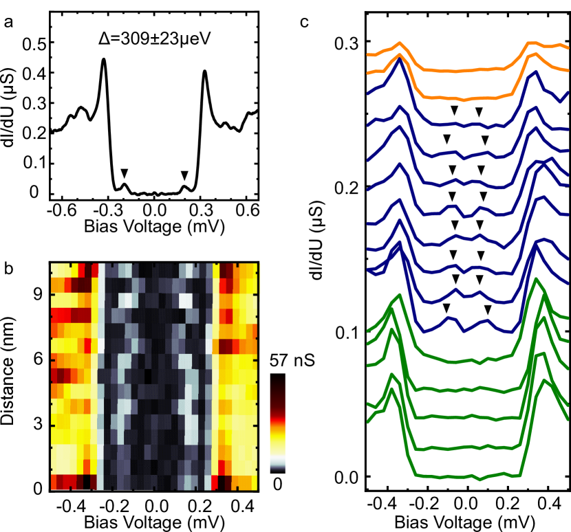
We now focus on the superconducting gap in oxygen rich samples. Figure 3a shows a high resolution spectrum of the superconducting gap with obtained from a BCS fit. The gap measured on different grains agrees within the error bar, and its value is slightly higher compared to the oxygen poor samples (cf. Fig. 1f). However, about half of the grains show in-gap states, as indicated by triangles in the spectrum of Fig. 3a. These states are of rather low intensity, but their energetic position rules out Andreev reflections of the tip electrons as their origin. Instead, the observation of the Kondo effect in grAl films above Moshe et al. (2018) suggests that unpaired electrons or magnetic moments give rise to Yu-Shiba-Rusinov (YSR) in-gap states. The energy of YSR states is a continuous function of the exchange coupling to the superconductor Farinacci et al. (2018), and of the charging energy of the grain or cluster of grains.
Similarly to Ref. Bachar et al. (2013), we consider two scenarios for the origin of the unpaired spins. First, the finite size of the grains and the fact that some are only weakly coupled to the rest of the grAl film might result in an odd number of charges on individual grains in equilibrium, as suggested by Deutscher et al. Moshe et al. (2018). The interaction of these unpaired electrons with the superconducting condensate may induce YSR states. Second, the non-stoichiometric composition of the AlOx in-between the pure Al grains may lead to unpaired electrons trapped in the insulating barriers. The interaction of these very localized states with the superconductor could be responsible for the measured YSR states.
In order to discriminate between the above scenarios, we measured the spacial dependence of the YSR states on a line crossing a single grain. While the superconducting gap remains constant, as shown in Fig. 3b, the in-gap states vary in energy as a function of the STM tip position. In the scenario of electrically decoupled grains with an odd number of electrons, the electric field of the STM tip would change the chemical potential of the grain, the coherence peaks would shift with tip position, but the energy of the YSR states with respect to the gap edge would be fixed. This is in contrast with our observations. If the unpaired spins reside in the oxide, the electric field of the tip can change their energy, and consequently the exchange coupling to the grain, as in the study of Farinacci et al. Farinacci et al. (2018). In this case the YSR state shifts with tip position, while the coherence peaks remain unaffected. This scenario agrees with our measurements. Moreover, Fig. 3c illustrates the strong localization of the YSR states on particular grains. Only the middle grain (blue spectra) shows in-gap states at (triangle markers).
In summary, using STM spectroscopy we have observed an enhanced and isotropic superconducting gap for both oxygen poor and rich grAl samples. In the oxygen rich samples the grains start to decouple, charging effects set in, eventually leading to the SIT. Hand in hand with this decoupling, we observed a secondary gap and excitations with an energy comparable to the superconducting gap, as well as YSR states in some of the grains, possibly related to unpaired electrons in the oxide barriers. For the YSR states to exist, the localized spins in the oxide need to exchange couple with the superconducting grain. If the oxide is sufficiently thin, the states in the oxide delocalize and we do not observe in-gap states. This interpretation is consistent with the fact that the YSR states appear only when the grains start to decouple, for resistivities larger than the Mott resistivity .
The existence of in-gap YSR states can be detrimental for grAl quantum devices in several ways: they can introduce additional dissipation in the microwave domain, or even alter the spectrum of the devices, if they couple sufficiently strong Grabovskij et al. (2012). The presence of spins may also contribute to the flux noise observed in grAl devices Grünhaupt et al. (2019), and more generally in pure Al devices, where these spins can form in the natural oxide at the surface and in the Josephson junction barrier. Further work should focus on measuring the density of YSR states versus resistivity in grAl, and also in native Al oxide, with the goal of reducing their impact on coherence in quantum devices.
References
- Cohen & Abeles 1968 Cohen, R. W. & Abeles, B. Superconductivity in granular aluminum films. Phys. Rev. 168, 444 (1968).
- Deutscher et al. 1973 Deutscher, G., Fenichel, H., Gershenson, M., Grünbaum, E. & Ovadyahu, Z. Transition to zero dimensionality in granular aluminum superconducting films. J. Low Temp. Phys. 10, 231 (1973).
- Grünhaupt et al. 2019 Grünhaupt, L. et al. Granular aluminium as a superconducting material for high-impedance quantum circuits. Nat. Mater. 18, 816 (2019).
- Valenti et al. 2019 Valenti, F. et al. Interplay between kinetic inductance, nonlinearity, and quasiparticle dynamics in granular aluminum microwave kinetic inductance detectors. Phys. Rev. Applied 11, 054087 (2019).
- Hazard et al. 2019 Hazard, T. et al. Nanowire superinductance fluxonium qubit. Phys. Rev. Lett. 122, 010504 (2019).
- Zhang et al. 2019 Zhang, W. et al. Microresonators fabricated from high-kinetic-inductance aluminum films. Phys. Rev. Applied 11, 011003 (2019).
- Pracht et al. 2016 Pracht, U. S. et al. Enhanced Cooper pairing versus suppressed phase coherence shaping the superconducting dome in coupled aluminum nanograins. Phys. Rev. B 93, 100503 (2016).
- Levy-Bertrand et al. 2019 Levy-Bertrand, F. et al. Electrodynamics of granular aluminum from superconductor to insulator: Observation of collective superconducting modes. Phys. Rev. B 99, 094506 (2019).
- Anderson 1958 Anderson, P. W. Absence of diffusion in certain random lattices. Phys. Rev. 109, 1492 (1958).
- Sacépé et al. 2008 Sacépé, B. et al. Disorder-induced inhomogeneities of the superconducting state close to the superconductor-insulator transition. Phys. Rev. Lett. 101, 157006 (2008).
- Sacépé et al. 2011 Sacépé, B. et al. Localization of preformed Cooper pairs in disordered superconductors. Nat. Phys. 7, 239 (2011).
- Driessen et al. 2012 Driessen, E. F. C., Coumou, P. C. J. J., Tromp, R. R., de Visser, P. J. & Klapwijk, T. M. Strongly disordered TiN and NbTiN s -wave superconductors probed by microwave electrodynamics. Phys. Rev. Lett. 109, 107003 (2012).
- Mondal et al. 2011 Mondal, M. et al. Phase fluctuations in a strongly disordered s-wave NbN superconductor close to the metal-insulator transition. Phys. Rev. Lett. 106, 047001 (2011).
- Mott 1968 Mott, N. F. Metal-insulator transition. Rev. Mod. Phys. 40, 677 (1968).
- Dynes et al. 1984 Dynes, R. C., Garno, J. P., Hertel, G. B. & Orlando, T. P. Tunneling study of superconductivity near the metal-insulator transition. Phys. Rev. Lett. 53, 2437 (1984).
- Bachar et al. 2013 Bachar, N., Lerer, S., Hacohen-Gourgy, S., Almog, B. & Deutscher, G. Kondo-like behavior near the metal-to-insulator transition of nanoscale granular aluminum. Phys. Rev. B 87, 214512 (2013).
- Bachar et al. 2015 Bachar, N. et al. Mott transition in granular aluminum. Phys. Rev. B 91, 041123 (2015).
- Moshe et al. 2019 Moshe, A. G., Farber, E. & Deutscher, G. Optical conductivity of granular aluminum films near the Mott metal-to-insulator transition. Phys. Rev. B 99, 224503 (2019).
- Feigel’man & Ioffe 2018 Feigel’man, M. V. & Ioffe, L. B. Microwave properties of superconductors close to the superconductor-insulator transition. Phys. Rev. Lett. 120, 037004 (2018).
- Kuzmin et al. 2019 Kuzmin, R. et al. Quantum electrodynamics of a superconductor–insulator phase transition. Nat. Phys. 930 (2019).
- Beloborodov et al. 2007 Beloborodov, I. S., Lopatin, A. V., Vinokur, V. M. & Efetov, K. B. Granular electronic systems. Rev. Mod. Phys. 79, 469 (2007).
- Dynes & Garno 1981 Dynes, R. C. & Garno, J. P. Metal-insulator transition in granular aluminum. Phys. Rev. Lett. 46, 137–140 (1981).
- Sherman et al. 2015 Sherman, D. et al. The Higgs mode in disordered superconductors close to a quantum phase transition. Nature Physics 11, 188 (2015).
- Nakamura et al. 2019 Nakamura, S. et al. Infrared activation of the Higgs mode by supercurrent injection in superconducting NbN. Phys. Rev. Lett. 122, 257001 (2019).
- Maleeva et al. 2018 Maleeva, N. et al. Circuit quantum electrodynamics of granular aluminum resonators. Nat. Commun. 9, 3889 (2018).
- Krantz et al. 2019 Krantz, P. et al. A quantum engineer’s guide to superconducting qubits. Appl. Phys. Rev. 6, 021318 (2019).
- Grabovskij et al. 2012 Grabovskij, G. J., Peichl, T., Lisenfeld, J., Weiss, G. & Ustinov, A. V. Strain tuning of individual atomic tunneling systems detected by a superconducting qubit. Science 338, 232 (2012).
- Wang et al. 2014 Wang, C. et al. Measurement and control of quasiparticle dynamics in a superconducting qubit. Nat. Commun. 5, 5836 (2014).
- Bachar et al. 2018 Bachar, N. et al. Kubo spins in nano-scale aluminum grains: A muon spin relaxation study. arXiv:1803.03177 (2018).
- Balashov et al. 2018 Balashov, T., Meyer, M. & Wulfhekel, W. A compact ultrahigh vacuum scanning tunneling microscope with dilution refrigeration. Rev. Sci. Instrum. 89, 113707 (2018).
- Douglass & Meservey 1964 Douglass, D. H. & Meservey, R. Energy gap measurements by tunneling between superconducting films. I. Temperature dependence. Phys. Rev. 135, A19 (1964).
- Hong et al. 2013 Hong, I.-P., Brun, C., Pivetta, M., Patthey, F. & Schneider, W.-D. Coulomb blockade phenomena observed in supported metallic nanoislands. Front. Phys. 1, 13 (2013).
- Winkel et al. 2019 Winkel, P. et al. Implementation of a transmon qubit using superconducting granular aluminum. arXiv:1911.02333 (2019).
- Friedrich et al. 2019 Friedrich, F. et al. Onset of phase diffusion in high kinetic inductance granular aluminum micro-SQUIDs. Supercond. Sci. Technol. 125008 (2019).
- Moshe et al. 2018 Moshe, A., Bachar, N., Lerer, S., Lereah, Y. & Deutscher, G. Multi-level Kondo effect and enhanced critical temperature in nanoscale granular Al. J. Supercond. Nov. Magn. 31, 733 (2018).
- Farinacci et al. 2018 Farinacci, L. et al. Tuning the coupling of an individual magnetic impurity to a superconductor: quantum phase transition and transport. Phys. Rev. Lett. 121, 196803 (2018).
- Pfeiffera & Schooleya 1969 Pfeiffera, E. R. & Schooleya, J. F. Superconducting transition temperatures of Nb-doped SrTiO3. Phys. Lett. A 29, 589 (1969).
Methods The samples consists of thick grAl films deposited by electron beam evaporation of pure Al at a rate of in an oxygen atmosphere, at a pressure in the range (c.f. Refs. 2, 3, 8). During the deposition the substrate is at room temperature. The resistivity of the films used in this work is in the to range, corresponding to a superconducting critical temperature near (c.f. SI). For these types of films, the SIT is observed for a room temperature resistivity . We used Nb doped (0.7 weight %) StTiO3 (Nb:STO) single crystals as substrates, in order to start off with a conducting, flat, and non-reactive surface. The substrate is expected to become superconducting at temperatures below 200 mK 37. Since the film thickness is much larger than the grain size of 2, the films show a bulk-like behaviour, i.e. most of the grains reside inside the film and determine the transport properties. It is therefore not surprising that the measured properties of grAl films are consistent between various substrates, such as glass, silicon or sapphire 2, 8. Immediately after deposition, in order to avoid surface oxidation of the grAl films, the samples were transferred to the ultra high vacuum of the STM using a vacuum suitcase, at a pressure in the range. STM measurements were carried out at a base temperature of 30 mK. If other temperatures were used, it is indicated in the figure captions.
Acknowledgements W.W. acknowledges funding by the Deutsche Forschungsgemeinschaft (DFG) under the grant WU 349/12-1 and INST 121384/30-1 FUGG. I.M.P and L.G. acknowledge the Alexander von Humboldt Foundation in the framework of a Sofja Kovalevskaja award endowed by the German Federal Ministry of Education and Research. F.Y. acknowledges funding from the Alexander von Humboldt foundation.
Author contribution F.Y., I.M.P. and W.W. conceived the experiments. F.Y., T.S. and T.G. carried out the STM experiments and analyzed the data. I.M.P. and L.G. grew the samples. F.Y., W.W., L.G., and I.M.P. wrote the draft. All authors contributed in discussions and finalizing the manuscript.