Infrared spectroscopic study of carrier scattering in gated CVD graphene
Abstract
We measured Drude absorption of gated CVD graphene using far-infrared transmission spectroscopy, and determined carrier scattering rate () as function of the varied carrier density (). The -dependent was obtained for a series of conditions systematically changed as (10 K, vacuum) (300 K, vacuum) (300 K, ambient pressure), which reveals that (1) at low-T, charged impurity () and short-range defect () are the major scattering sources which constitute the total scattering , (2) among various kinds of phonons populated at room-, surface polar phonon of the SiO2 substrate is the dominantly scattering source, (3) in air, the gas molecules adsorbed on graphene play a dual role in carrier scattering as charged impurity center and resonant scattering center. We present the absolute scattering strengths of those individual scattering sources, which provides the complete map of scattering mechanism of CVD graphene for the first time. This scattering map allows us find out practical measures to suppress the individual scatterings, the mobility gains accompanied by them, and finally the ultimate attainable carrier mobility for CVD graphene.
pacs:
68.65.Pq 78.30.-j 78.67.WjIntroduction
Two dimensional (2D) graphene has been extensively studied during recent years because of its fundamental interest and device applications. The latter one was highlighted with particular attention by the successful synthesis of the large scale graphene by use of the chemical vapor deposition (CVD) method.kim2009large ; bae2010roll ; lee2010wafer ; li2009large The CVD graphene with wafer-scale size, often as large as 30-inch, bae2010roll opened a route to practical application of graphene as various devices such as flexible display. However, despite the great merit in the large size, CVD graphene exhibits carrier mobility which is definitely low compared with that of the exfoliated graphene, indicating that the Dirac electron (hole) experiences more scattering in the former one. For the CVD graphene supported by substrate, the carrier is scattered by various kinds of scattering sources. To name some of them, impurity and defect are created during the growth, transfer, and device fabrication of graphene. Pseudomagnetic field due to random strain produces another scattering channel to carrier. Cuoto The acoustic- and optical-phonons are thermally populated in the graphene and also in the substrate, which scatter the carrier through the electron-phonon interaction.hwang2008acoustic ; zou2010deposition ; chen2008intrinsic Furthermore, when the graphene device is operated in ambient condition, air molecules adhere to graphene and scatter the carrier.robinson2008adsorbate ; wehling2009adsorbates
In order to improve the mobility of CVD graphene, a thorough knowledge must be gained on the carrier scattering mechanism. Specifically one should identify all the scattering sources participating in the carrier scattering, determine their precise scattering strengths in terms of well-defined quantity such as the scattering rate, find out the practical ways of removing or reducing the scattering sources, and finally, based on these investigations, should present the highest mobility value that can be achieved in the scattering-suppressed CVD graphene. To this end, extensive experimental efforts must be devoted, which has been lacking to date. To perform such experiment one should take special care to choose a measurement tool that can effectively probe the carrier scattering and mobility. In particular, because the carrier mobility is determined by the carrier density and scattering rate in graphene as , it is desirable that the tool is capable of detecting and simultaneously in a single measurement. Also, noting that various kinds of scatterings are mixed together in graphene sample, one should devise a strategy to disentangle them and measure the individual scattering strengths separately.
In this work we perform a Far-infrared (FIR) transmission experiment of CVD graphene supported on SiO2/Si substrate. The FIR spectroscopy, a remote and contactless probe of carrier dynamics, measures Drude response of the Dirac carrier. The strong merit of measuring the Drude peak is that and are measured simultaneously, allowing us figure out the relationship between them, . We show that the scattering function , obtained for a range of by electrostatically gating the device, provides the key to identify the scattering sources and determine their scattering strengths.
Experiment
A CVD-grown graphene, 5 mm by 5 mm in size, was transferred on SiO2/Si substrate li2009large and the sample was mounted in a temperature-variable (10 K 300 K) transport/optical dual purpose cryostat and treated by thermal annealing (350 oC, 1.5 h) in vacuum (10-6 Torr). The transport - curve and FIR optical transmission were measured for the same sample as gating voltage was applied to graphene for the hole-doping and then electron-doping regime. A commercial FTIR (Bomem DA8) and He-cooled bolometer were used for the FIR measurement. We used the RefFit-program to rigorously analyze FIR-data for quantitative analysiskuzmenko2005kramers .
Results and discussion
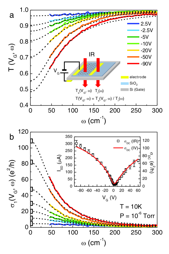
Figure 1(a) shows taken at K and Torr. Gating voltage was applied into the hole-doping regime V. The free carrier absorption becomes stronger as more carrier is induced in graphene with increasing . We calculate the optical conductivity by applying the Kramers-Kronig constrained variational method to kuzmenko2005kramers . For quantitative analysis we fit using the Drude model
| (1) |
where DC-conductivity and carrier scattering rate are the fitting parameters. The fitting curves show good agreement with data [Fig. 1(b)]. In the inset we compare the FIR- with transport where the latter is extracted from - data using the relation , = channel length and = channel width. The two results are in good agreement, confirming the consistency between our transport and optical experiments. The - curve shows that the charge neutral voltage is very low ( V), the curve is fairly symmetric for the hole- and electron-doping, and the carrier mobility is reasonably high ( at V), demonstrating high quality of our sample. FIR-data for the electron-doping regime is presented in Supplementary, Fig. S1.
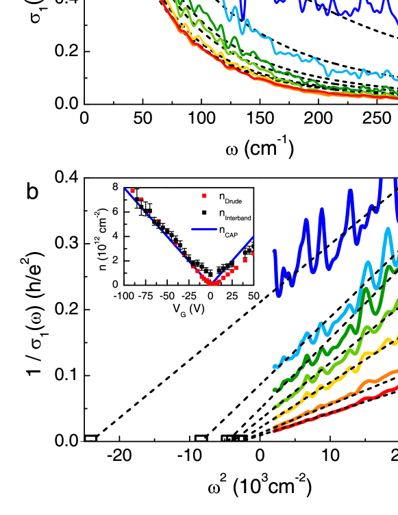
Fig. 2(a) shows how changes with . Here we plot , the normalized by . corresponds to the curve width measured at half maximum . is large at low doping and decreases as increases. To double-check this behavior of , we seek another way of data analysis: From Eq. (1), it follows that
| (2) |
where , . The linear dependence of on is confirmed in Figure 2(b). By performing linear-fit of data, we obtain the slope () and -intercept (), from which and are calculated. They reproduce the results of Fig.2(a). For later comparison of data with theory, we convert the .vs. relation into .vs.. For this end we calculate carrier density for each using the relation where , . Note that can be measured alternatively from the Drude weight and also from interband optical transition (Supplementary Fig. S3).
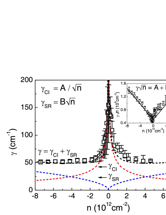
In Fig. 3 we show . The electron-doping regime is included in this plot. For graphene impurity and defect are inevitably introduced during the growth and they produce major scattering at low temperature like in other solids. For a charged-impurity (CI) decreases as increases due to screening of the Coulomb potential, = / sarma2011electronic ; hwang2007carrier . On the other hand, charge-neutral defects are often described by the short-ranged (SR) potential and the scattering for this case increases as for 2D graphene sarma2011electronic ; hwang2007carrier . We assume that they coexist
| (3) |
and use Eq. (3) to fit our . The fit agrees reasonably well with data for hole-doping regime. To double-check the data fit we multiply to Eq. (3) which leads to . The linear behavior of with respect to is confirmed in the data (inset), and the coefficients , the -intercept) and , slope) are determined. For the electron-doping regime the data deviates from the fit, which indicates small amount of air or ice inevitably adsorbed on graphene at low-T (see Supplimentary VI for details). Eq. (3) predicts that should increase when is very high due to the term. Recently we measured the FIR- up to 3 1013 using the electronic double layer (EDL) gating and found that indeed increases as predicted. In the 2D scattering theory and are given as and , where and are the density of the CI and the SR respectively, and is the potential strength of the SR. Comparison with our experimental and shows that cm-2 and (eVÅ)2. As for , the exact potential strength is not known can not be determined. However, of our sample is about 10 times stronger than the of high mobility exfoliated graphene hwang2007carrier indicating that SR is significant in CVD graphene.
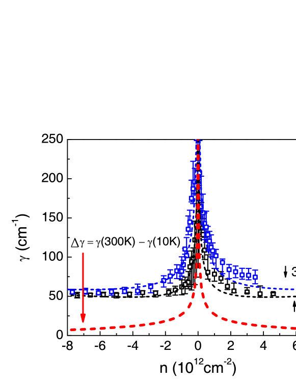
Next we increase the sample temperature to K and repeat the -controlled FIR measurement. Figure 4 shows that has increased compared with K. We calculate -driven scattering rate which decreases with increasing (red curve). At room-, phonons are populated in graphene and substrate. In graphene, acoustic phonons (AP) and optical phonons (OP) create the phonon-carrier scattering with the rates cm-1 ( is the measured in cm-2) and (independent of ) respectively hwang2008acoustic . Obviously they do not account for in terms of the -dependence. As for the SiO2 substrate, optical phonon in conjunction with the polar-discontinuity produces the surface polar phonon (SPP) scattering to graphene. Because the SPP has the nature of the long-range Coulomb interaction, it is screened by carrier in graphene and decresaes with increasing . In Ref. 16 authors calculated to plot other quantaties such as the dc-conductivity. We compared it with our which showed that they agree in their -dependent behaviors, i.e, the sharp increase of scattering with in the vicinity of =0, leading to the conclusion that SPP of the substrate is the main scattering source among other temperature-induced scatterings.
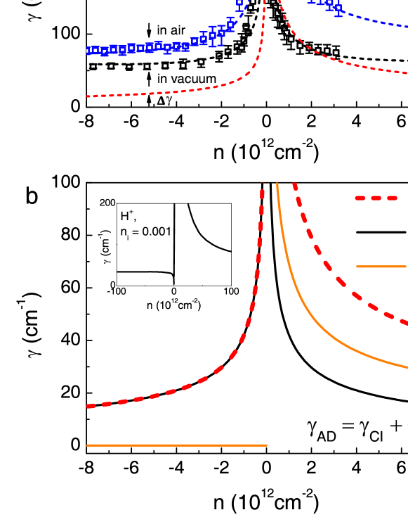
In ambient condition air molecules adhere to graphene and become a scattering sources. To study this scattering effect, we purged the sample chamber with air at K. The - curve shifts to positive along with the elapse of time, indicating that graphene is progressively doped by hole [inset of Fig. 5(a)]. After the - shift has saturated we measured FIR- and calculated the adsorbate scattering (AD) . Figure 5(a) shows that is asymmetric for the hole-doping and electron-doping. We propose that consists of two components as where is the CI-scattering as we discussed above, and is a scattering of unknown origin at this point. The - shift (or hole-doping) implies that Dirac electron in graphene moves to the adsorbed gas. The adsorbate is then negatively charged, behaving as a CI-scatterer to graphene. For hole-doping regime , can be fit with the CI-scattering alone [Fig. 5(b)], i.e, ( cm-2) and . For the electron-doping non-zero is needed in addition to to fit data. shows the -dependent shape of this scattering (black curve). Robinson et al. studied theoretically the orbital hybridization of graphene and adsorbate, revealing that carrier in graphene undergoes a resonant behavior when scattered by the hybridized orbital robinson2008adsorbate . They showed that the resonant scattering is highly asymmetric for the hole and electron carrier. For instance we reproduce one of their results in the inset of Fig. 5(b), which is almost zero for hole and strong for electron, consistent with our experimental . Based on this observation we assign to and propose that adsorbate plays the dual role as Coulomb scatterer and the resonant scatterer.
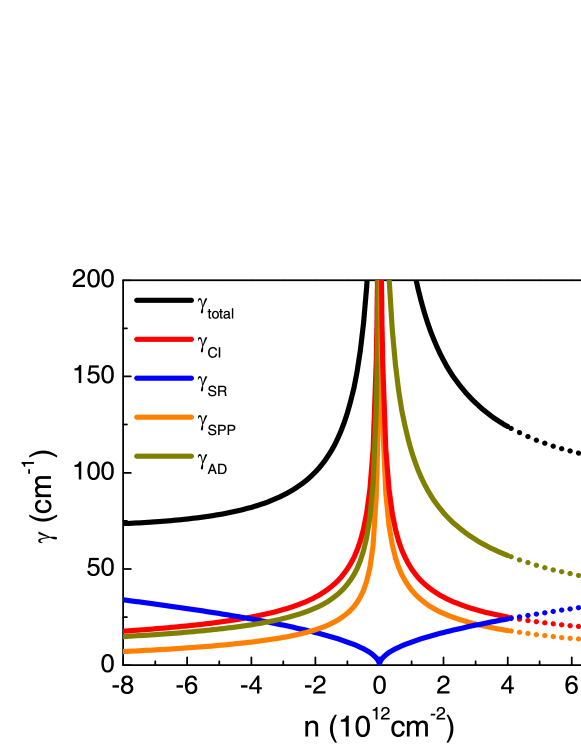
In Fig. 6 we plot all ’s determined in this work in one graph. It shows quantitatively how the total scattering is composed in terms of the individual scatterings. For example, at a moderate hole-doping cm-2, the four scatterings contribute to in ratio. For electron-side cm-2 the ratio changes to . In graphene the carrier mobility is determined from and , where the Fermi velocity is cm/s. For the FET operated at K and in air, cm-1 from Fig. 6 and we have cm2/Vs (we take cm-2 again). How can one improve the mobility to higher value? If we assume the impurity and defect could be reduced to the quality of exfoliated graphene through the advances of growth technique, the single-crystal CVD graphene being one recent example of them lee2014wafer , then can be reduced from current value 52.4 cm-1 to 17.7 cm-1 tan2007measurement . In terms of the total , is reduced from 100.5 cm-1 to 65.8 cm-1 and increases to 5340 cm2/Vs. For further improvement we note that can be reduced by employing a substrate with high energy optical phonon. For example hexagonal boron nitride (hBN) has optical phonon at meV geick1966normal , higher than meV of SiO2. As result the number of thermal populated SPP, , decreases by 1/72 of that for SiO2. If we assume is proportional to it is reduced from cm-1 (Fig. 6) to cm-1. The total scattering decreases to = 47.7 cm-1 leading to the enhanced mobility cm2/Vs. Finally, as for , the gas adsorption can be prevented by covering graphene with a proper passivation material. In fact hBN is an efficient passivator as proved for black phosphorus (BP) and MoS2doganov2015transport ; lee2015highly . If we assume that few-layer hBN is integrated with graphene it will suppress the adsorption scattering at the cost of another hBN ”substrate” scattering introduced from the top. For the hBN(top)/graphene/hBN(substrate)/Si total scattering + 2 hBN- (2 = top + bottom) is reduced to 18.3 cm-1, because hBN- (see Fig. 6), and the mobility is increased to cm2/Vs. We regard this value is probably the highest mobility one can practically achieve for room- and in-air FET operation. To make the suggested multi-stack structure, synthesis of high quality CVD hBN and integration technique of two CVD material sheets are necessary, which were demonstrated recently jang2016wafer ; kim2016chiral .
To conclude, we have obtained complete map of scattering mechanism of CVD graphene by performing FIR-transmission measurements. The four scattering sources were identified and their individual scattering strengths were measured. This quantitative and source-resolved scattering map (Fig. 6) provides insight into improved carrier mobility by (1) removing the impurity and defect in graphene and substrate, (2) inserting hBN layer between graphene and SiO2 substrate, (3) protecting graphene from air using hBN passivation, where the ultimate mobility is estimated to be cm2/Vs for practical device operation at room-T and in air. Our findings offer invaluable guide to the application of the large scale graphene as high-speed electronic device.
Acknowledgements
This work was supported by the National Research Foundation of Korea(NRF) grant funded by the Korea government(MSIP) (NRF-2014R1A2A2A01003448 and NRF-2014R1A2A 2A01006776 (E.H.H.)).
References
- (1) K. S. Kim, Y. Zhao, H. Jang, S. Y. Lee, J. M. Kim, K. S. Kim, J.-H. Ahn, P. Kim, J.-Y. Choi, and B. H. Hong, Nature 457, 706 (2009).
- (2) S. Bae, H. Kim, Y. Lee, X. Xu, J.-S. Park, Y. Zheng, J. Balakrishnan, T. Lei, H. R. Kim, Y. I. Song, Y.-J. Kim, K. S. Kim, B. Ozyilmaz, J.-H. Ahn, B. H. Hong, and S. Iijima, Nat. Nanotechnol. 5, 574 (2010).
- (3) Y. Lee, S. Bae, H. Jang, S. Jang, S.-E. Zhu, S. H. Sim, Y. I. Song, B. H. Hong, and J.-H. Ahn, Nano Lett. 10, 490 (2010).
- (4) X. Li, W. Cai, J. An, S. Kim, J. Nah, D. Yang, R. Piner, A. Velamakanni, I. Jung, E. Tutuc, S. K. Banerjee, L. Colombo, and R. S. Ruoff, Science 324, 1312 (2009).
- (5) N. J. G. Couto, D. Costanzo, S. Engels, D.-K. Ki, K. Watanabe, T. Taniguchi, C. Stampfer, F. Guinea, and A. F. Morpurgo, Phys. Rev. X 4, 041019 (2014).
- (6) E. H. Hwang and S. DasSarma, Phys. Rev. B 77, 115449 (2008).
- (7) K. Zou, X. Hong, D. Keefer, and J. Zhu, Phys. Rev. Lett. 105, 126601 (2010).
- (8) J.-H. Chen, C. Jang, S. Xiao, M. Ishigami, and M. S. Fuhrer, Nat. Nanotechnol. 3, 206 (2008).
- (9) J. P. Robinson, H. Schomerus, L. Oroszlany, and V. I. Falko, Phys. Rev. Lett. 101, 196803 (2008).
- (10) T. Wehling, M. Katsnelson, and A. Lichtenstein, Chem. Phys. Lett. 476, 125 (2009).
- (11) A. Kuzmenko, Rev. Sci. Instrum. 76, 083108 (2005).
- (12) S. DasSarma, S. Adam, E. H. Hwang, and E. Rossi, Rev. Mod. Phys. 83, 407 (2011).
- (13) E. H. Hwang, S. Adam, and S. DasSarma, Phys. Rev. Lett. 98, 186806 (2007).
- (14) E. H. Hwang and S. DasSarma, Phys. Rev. B 87, 115432 (2013).
- (15) J.-H. Lee, E. K. Lee, W.-J. Joo, Y. Jang, B.-S. Kim, J. Y. Lim, S.-H. Choi, S. J. Ahn, J. R. Ahn, M.-H. Park, C.-W. Yang, B. L. Choi, S.-W. Hwang, and D. W. Whang, Science 344, 286 (2014).
- (16) Y.-W. Tan, Y. Zhang, K. Bolotin, Y. Zhao, S. Adam, E. H. Hwang, S. DasSarma, H. L. Stormer, and P. Kim, Phys. Rev. Lett. 99, 246803 (2007).
- (17) R. Geick, C. Perry, and G. Rupprecht, Phys. Rev. 146, 543 (1966).
- (18) R. A. Doganov, E. C. OFarrell, S. P. Koenig, Y. Yeo, A. Ziletti, A. Carvalho, D. K. Campbell, D. F. Coker, K. Watanabe, T. Taniguchi, A. H. Castro Neto, and B. Ozyilmaz, Nat. Commun. 6, 6647 (2015).
- (19) G.-H. Lee, X. Cui, Y. D. Kim, G. Arefe, X. Zhang, C.-H. Lee, F. Ye, K. Watanabe, T. Taniguchi, P. Kim, and J. Hone, ACS nano 9, 7019 (2015).
- (20) A.-R. Jang, S. Hong, C. Hyun, S. I. Yoon, G. Kim, H. Y. Jeong, T. J. Shin, S. O. Park, K. Wong, S. K. Kwak, N. Park, K. Yu, E. Choi, A. Mishchenko, F. Withers, K. S. Novoselov, H. Lim, and H. S. Shin, Nano Lett. 16, 3360 (2016).
- (21) C.-J. Kim, A. Sanchez-Castillo, Z. Ziegler, Y. Ogawa, C. Noguez, and J. Park, Nat. Nanotechnol. 11, 520 (2016).