Topologically Enabled Ultralarge Purcell Enhancement Robust to Photon Scattering
Abstract
Micro/nanoscale single photon source is a building block of on-chip quantum information devices. Owing to possessing ultrasmall optical mode volume, plasmon structures can provide large Purcell enhancement, however scattering and absorption are two barriers to prevent them from being used in practice. To overcome these barriers, we propose the topological photonic structure containing resonant plasmon nanoantenna, where nanoantenna provides large Purcell enhancement while topological photonic crystal guides all scattering light into its edge state. Through the optical mode design, the rate of single photons emitted into the edge state reaches more than simultaneously accompanied with an obvious reduction of absorption. This kind of nonscattering large Purcell enhancement will provide new sight for on-chip quantum light sources such as a single photon source and nanolaser.
- Keywords
-
Topological photonic structrue; Plasmon nanoantenna; Purcell enhancement
I 1. Introduction
Micro/nanoscale single photon source is an indispensable building block of on-chip quantum information processing single-photon-1 ; single-photon-2 . Utilizing local field enhancement or high density of optical modes of photonic structures to improve the spontaneous emission of single emitter is one of key principles of realizing a single photon emission. Typical micro/nanostructures include whispering guided resonantors WGM1 , photonic crystals (PCs)CQED_PC1 ; CQED_PC2 ; CQED_PC3 , and plasmon nanostructures CQED_MNP4 ; CQED_MNP5 ; CQED_MNP6 . Though achieving large Purcell enhancement, the volume of whispering guided resonantor itself is at the microscale WGM1 , which to some extent prevents compact integration of on-chip. PC cavities can effectively increase the photon emission, but the emission rate is generally low CQED_PC1 ; CQED_PC2 ; CQED_PC3 . Owing to possessing ultrasmall optical mode volume, plasmon nanostructures can provide large Purcell enhancement CQED_MNP4 ; CQED_MNP5 ; CQED_MNP6 . However, their scattering and absorption are two barriers when guiding these single photons into other devices. To solve the problem of scattering, the gap surface plasmon structures are proposed by combining the advantages of effectively collecting scattering light by a nanowire or nanofilm and inducing large Purcell enhancement by plasmon nanoparticles Gu-1 ; Gu-2 ; Gu-3 . However, their collecting efficiency is not very high and it is almost impossible to reach 100 collecting of photons. Thus, the final part guided into other on-chip devices is very low and those stray light will severely affect the performance of neighbouring devices, which prevent them from being a good candidate to realize a high quality single photon source.
By introducing quantum Hall effect into optics, topological photonics becomes an important branch in micro/nano photonics 1 ; 2 ; 4 . Topological states are some specific optical modes existing between the optical bands, characterized as topological invariants in the reciprocal space chan-1 ; 3 ; 5 , such as Berry curvature, Berry phase, and Chern number. So those micro/nano structures with energy bands and gaps, such as photonic crystals 6 , coupled-resonator arrays 7 , and synthetic dimensions spatial-modal lattices 8 , are good candidates to realize the topological properties. Topological states, generally referring to edge states or interface states, are characterized as nonscattering propagation of photons and immunity to a wide class of impurities and defects, i.e., topological protection 3 ; 5 . These features allows to fabricate various micro/nano photonic devices, including topological lasers 9 ; 10 ; 11 , nonscattering sharp bent waveguides 12 ; 13 , and topological quantum light 14 . Recently, topological protection is utilized in on-chip quantum information processing, such as robust transport of entangled photons 15 , protection of biphoton states 16 , and topological phase transition in single-photon dynamics 17 . However, using topological protection into the Purcell enhancement has not been reported yet. Though overcoming the scattering problem in the propagation process, if only depending on edge states to improve Purcell enhancement, its emission rate can not be very high.
To the end of obtaining nonscattering Large Purcell enhancement, we propose a specific topological photonic structure, i.e., 1D topological PC containing a resonant nanoantenna [Fig. 1(a)]. By embedding an antenna into the topological PC, strong local field near antenna leads to a large Purcell enhancement while nonscattering edge state can make all scattering photons propagate along some specific direction. In condition of topological protection, through the frequency matching between resonant antenna and edge state, total Purcell factor can reach more than ( is the spontaneous emission rate in vacuum), among which the propagating part along the edge state channel is more than . Interestingly, there is an obvious absorption reduction in total Purcell enhancement due to the deformation of nearfield of nanoantenna caused by the edge state. Moreover, the Purcell factors are very sensitive to the nanoantenna size, relative position of nanoantenna and quantum emitter in topological PC. Through propagating those single photons along the edge state, scattering problem is solved, which will be directly used to on-chip quantum devices. This kind of nonscattering ultralarge Purcell enhancement will provide new sight for on-chip quantum light sources such as a single photon source and nanolaser.
II 2. Optical modes of topological photonic structures
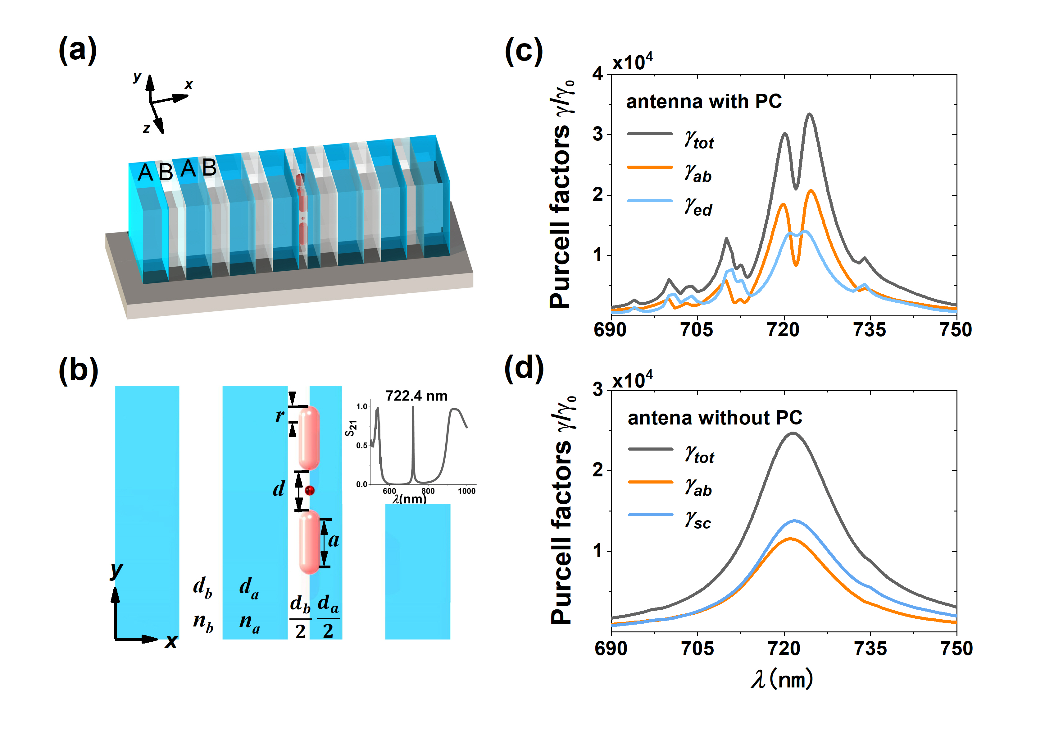
We choose 1D topological photonic structure composed of two semi-infinite PCs with layers A and B [Fig. 1(a)]. This kind of topological PC, characterized as Zak phase, was proposed by Chan et al. chan-1 . And then the concept of Zak phase was extended to various 2D photonic structures chan-2 ; chan-3 ; chan-4 ; chan-5 and applicated in topological light-trapping NC-trapping and nanolaser CP . However, nonscattering propagation in edge state has not been brought into the Purcell enhancement. The edge state in a dielectric PC is a bulk mode, so its Purcell factor can not be very large, generally dozens of supple . While resonant metallic nanopartice with strong local field can take great Purcell enhancement CQED_MNP4 ; CQED_MNP5 ; CQED_MNP6 . However, due to the loss of absorption and scattering, the single photons dispersing around the nanoparticle is difficult to be utilized. Therefore, by combining the advantages of the topological PC and plasmon nanoparticle, we design the topological photonic structure containing 1D PC and metallic nanoantenna [Fig. 1(a)]. With this structure, we obtained large Purcell factors, among which all scattering part of single photons is guided into the edge state. Owing to the small size of nanoantenna, in the following computation, the topological protection of whole structure is conserved supple .
If now putting a quantum emitter into the near field region of nanoparticle, total Purcell enhancement can be divided into three parts, i.e., , where is the absorption part, the decay rate into the edge state, and radiative part into free space. It is different from that the metallic nanoparticle is embedded in the dielectric, where , among which is the scattering part into the free space and can not be effectively collected CQED_MNP4 ; CQED_MNP5 ; CQED_MNP6 . In topological PC, if the metallic nanoparticle is small enough, can be neglected due to topological protection from impurities. For our designed topological photonic structure, the part of is totally suppressed while the part of collects all the scattering photons supple , i.e., is validated. Thus single photons from the part can be used in the on-chip photonic devices with nonscattering.
As shown in Fig. 1(b), the topological 1D PC consists of two semi-infinite PCs of two layers A and B with the thickness of =120 nm and =100 nm and the refractive index of =2 and =1. With these parameters, the edge state appears at the wavelength of 722.4 nm shown as the inset of (b). The nanoantenna with the resonant wavelength of 722.4 nm is horizontally placed into the interface of two semi-infinite PCs. The spectral linewidth of edge state and surface plasmon of nanoantenna are 2.7 nm and 18.8 nm respectively. A quantum emitter is set at the nanoscale gap of antenna. To compute the Purcell factors of above topological structure, 3D finite-element simulations were performed using COMSOL Multiphysics software, through which we have simulated optical modes, Purcell enhancement, photon collection, and photon-emitter coupling strength for various photonic structures Gu-NN ; Gu-1 ; Gu-2 ; Gu-3 ; Gu-4 ; Gu-5 . To simulate the infinite 1D PC, periodic boundary condition is applied for the vertically directional boundary of propagation. In the direction of photonic propagation, 5 periods for both sides of semi-infinite photonic crystal are enough to perform infinite-like behavior. The emitter is represented by a polarized dipole point source. Computation details of , , , and are shown in Ref. supple . In the supplementary materials, we have proved no scattering part through the four boundary of propagation because of the topological protection as well as the correctness and validity of above module.
III 3. Results and discussions
III.1 3.1 Nonscattering ultralarge Purcell enhancement at edge state
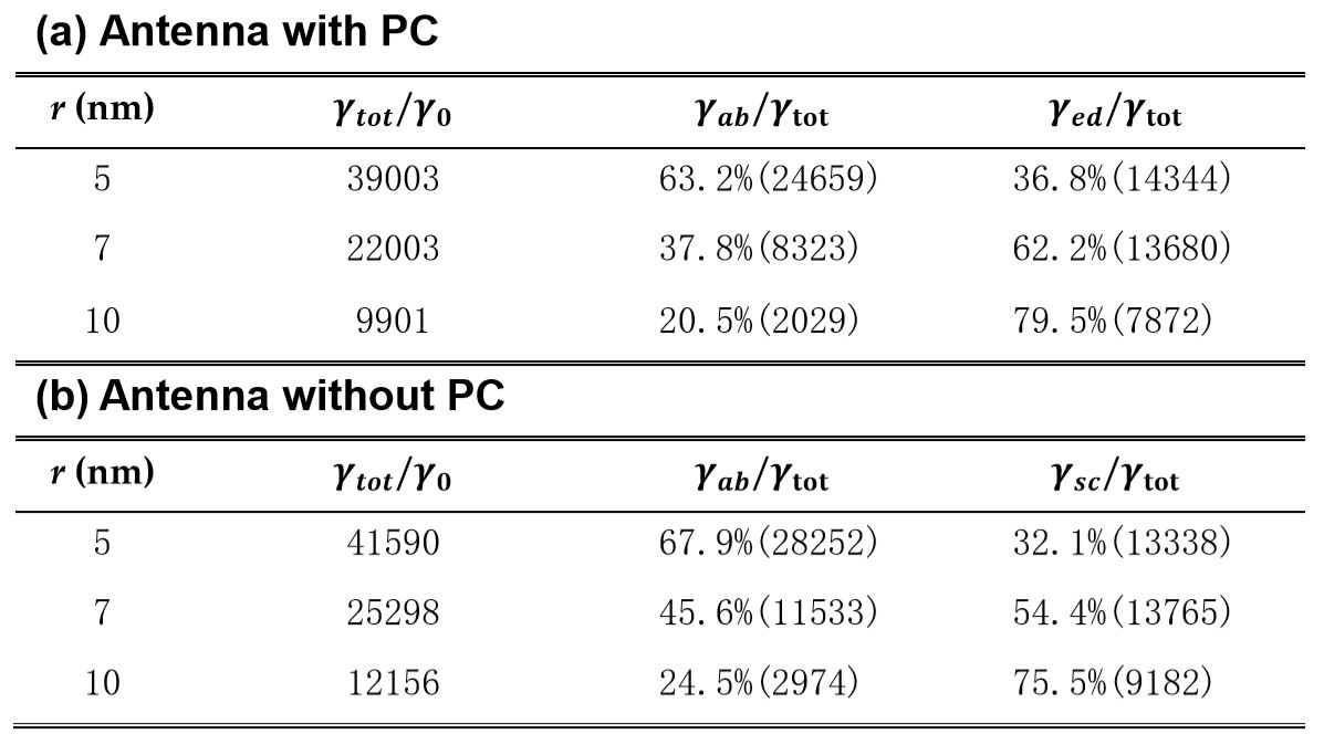
Nonscattering Purcell enhancement of topological PC containing the Ag nanoantenna is investigated. As shown in Fig. 1(c), total Purcell factor can reach more than , among which the part guided into the edge state is . Here, the parameters of silver nanoantenna are 7 nm, 24.45 nm, and 10 nm. Owing to the topological protection, there is almost not any photon scattering. At the edge state of =722.4 nm, which is also corresponding to the resonant wavelength of Ag nanoantenna, there is a dip in the spectra of and , and is in its minimum while the reaches its maximum. This ultralarge nonscattering enhancement is superior to that of gap surface plasmon structures, where the Purcell factor is also very large, but the guided part is relatively small and the stray light exists Gu-1 ; Gu-2 ; Gu-3 . The linewidth of is greatly less than that of due to the decoupling bewteen the 1D PC and Ag nanorod. It is also found that, at the edge state, the ratio of (37.8) in topological structure is less than that of (45.6) in dielectric [Figs. 1(c, d)], which means an obvious absorption reduction due to the existence of edge state.
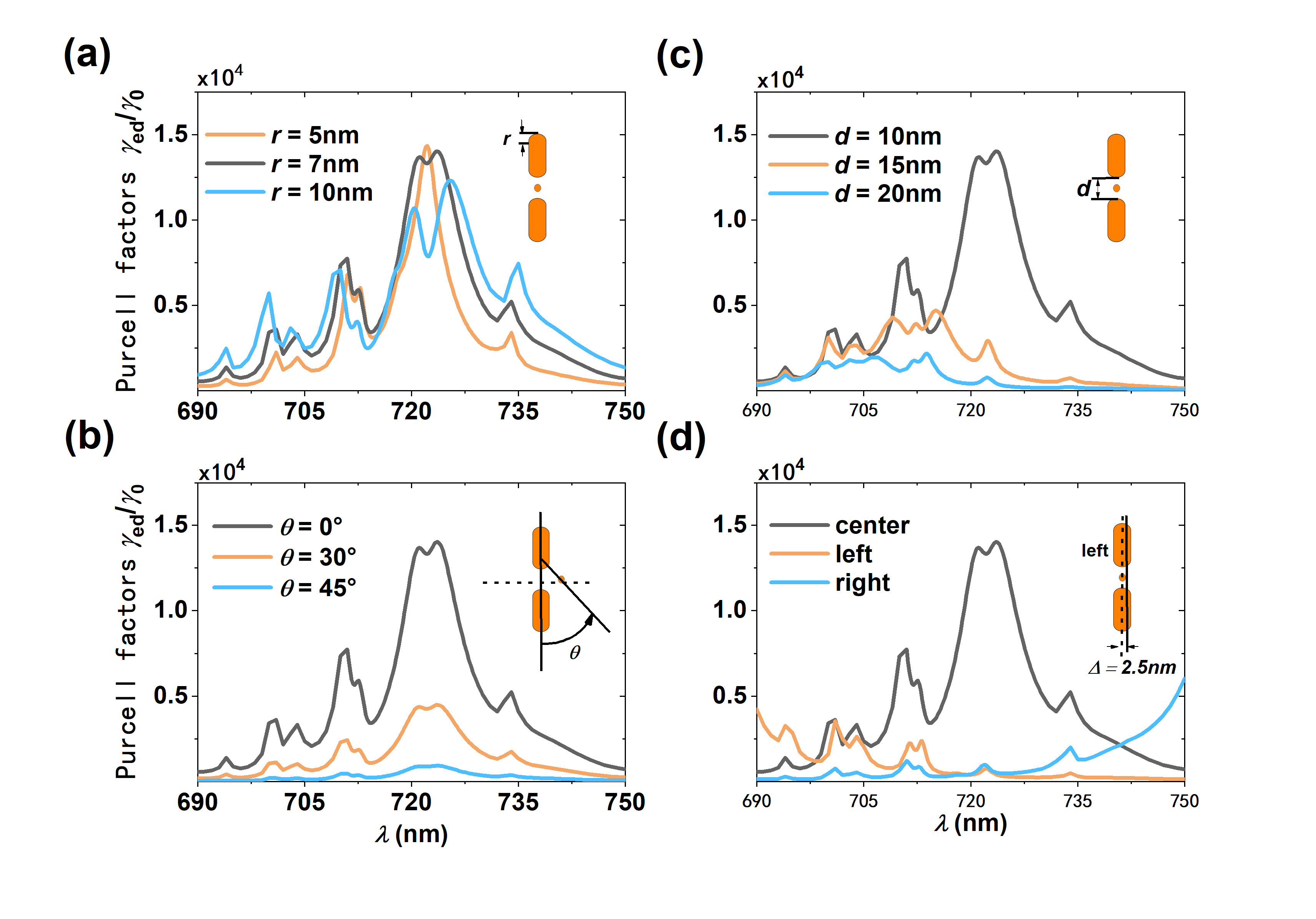
Then, we focus our attention on the nonscattering Purcell factors for various parameters of nanoantenna embedded in topological PC. While keeping the resonance matching between the edge state and resonant antenna, let us explore the effect of varying nanorod radius and emitter position on . When the radius is smaller, both and become larger due to more localized electric field [Fig. (2a)]. We also changed the relative angle between the emitter and nanoantenna [Fig. (2b)]. It is found that away from near field region, such as , decreases abruptly. This is similar to the case of resonant metallic nanorod embedded in the dielectric medium, where the position of the emitter is very sensitive to the scattering part CQED_MNP4 ; CQED_MNP5 ; CQED_MNP6 . In the near field region, the ratios of in topological structure and in dielectric medium keep almost as a constant respectively. But away from the near field region, these ratios as well as descend abruptly. More computation details are shown in the Ref. supple . Therefore, by changing the structure parameters of nanoantenna or the position of emitter, the magnitude of nonscattering part as well as can be well modulated.
Owing to narrow linewidth of the edge state, Purcell enhancement is very sensitive to resonance matching between the nanorod and edge state. When the gap distance of nanoantenna is changed from 10 nm to 15 nm, decreases greatly due to off resonance condition [Fig. 2(c)]. If we slightly move the position of nanoantenna away from the the center of two PC layers, there is a great decrease in due to the red and blue shift of resonance wavelength [Fig. 2(d)]. Thus, Purcell enhancement in this topological photonic structure is in a large extent determined by the resonance matching.
With the resonance matching condition, we also study the Purcell enhancement in this topological PC containing other kinds of nanoparticles, such as a single nanorod lying parallel to the interface, a single nanorod being vertical to the interface, and the antenna being vertical to the interface supple . It turns out that as long as the topological protection is conserved, the equation =+ is satisfied and large nonscattering Purcell enhancement is maintained. Overall, structures of antenna have a larger Purcell enhancement than those of single nanorod, and structures that lies parallel to the interface have larger ratio of /. It means that the edge state can greatly change the local field of nanoparticle and then changed local field further influences the Purcell factors , and . These results are helpful to experimental realization of this protocol.
III.2 3.2 Absorption reduction induced by edge state
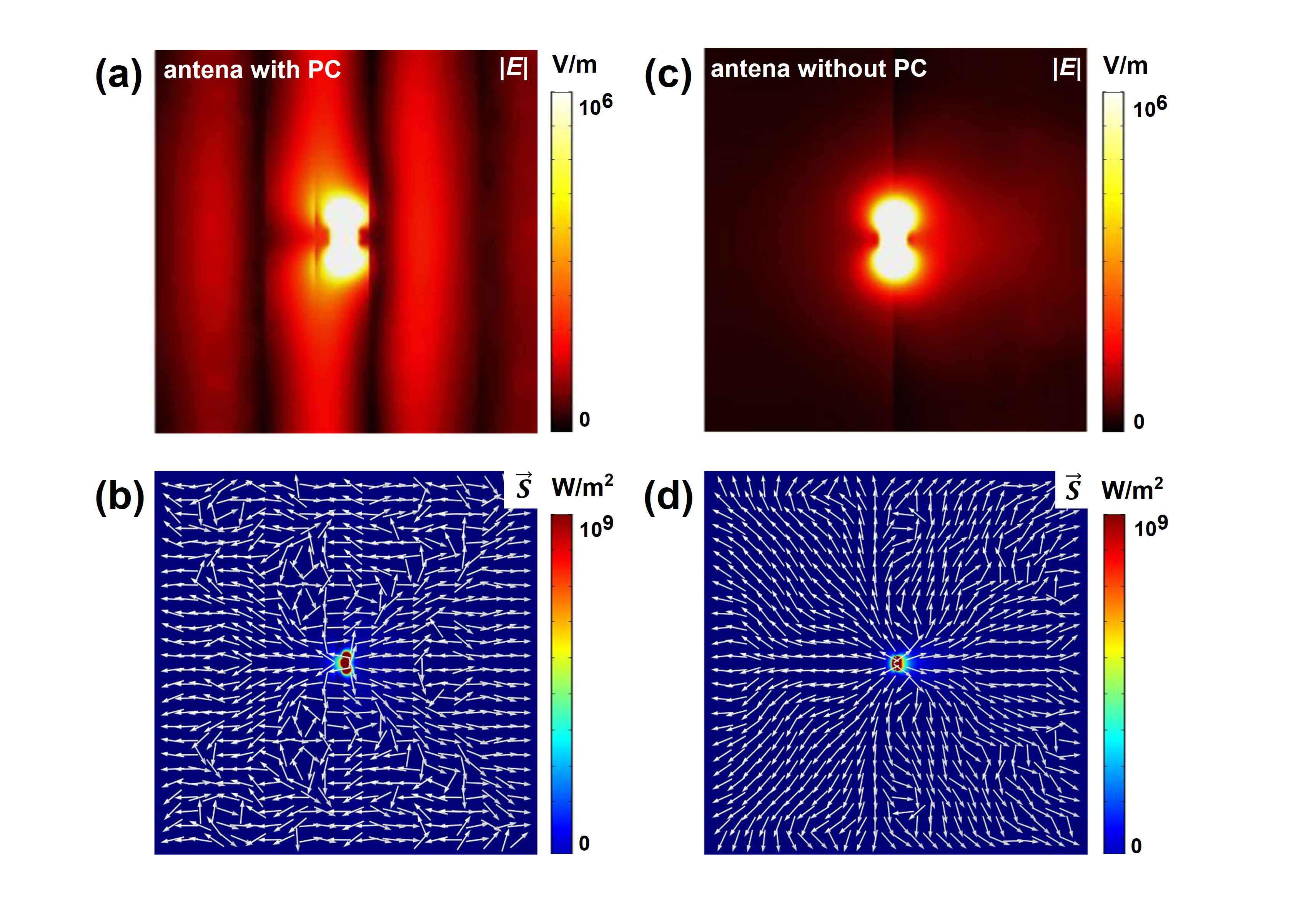
Let us look back to the dip (corresponding to edge state) in the spectra of Purcell factors and in Fig. 1(c). As shown in Figs. 3(a, b), both the electric field and energy flux for the nanoantenna in the topological structure are drawn away by the edge state comparing with the case of the nanoantenna in the dielectric [Figs. 3(c, d)]. In topological structures, the near field is not localized as that without PC, thus a little decreased is obtained. According to the electromagnetic boundary condition, in this case the electric field of nanoantenna becomes weaker than that in dielectric medium, leading to the reduction of absorption. Simultaneously, the energy flux in topological structure is flowing along the PC directionally [Figs. 3(b)], while the energy flux in dielectric medium scatters into all directions [Figs. 3(d)].
Next we pay attention to the radios of and at the edge state. As shown in Tab. 1, the radio of (37.8 for nm ) in topological structure becomes smaller, and correspondingly, its edge state part (62.2) gets larger, comparing with the same size antenna in the dielectric where and separately. So this is an obvious absorption reduction in Purcell enhancement.
Moreover, absorption reduction with other size of nanoantenna is also investigated [Tab. 1]. Here the distance between two nanorods is fixed at nm and resonance matching condition is kept. First, whether there is a topological structure or not, the ratio of is smaller when becomes larger due to less localized field (or larger optical mode volume). However, for the same , this ratio in topological structure is smaller than that in dielectric medium, namely, it is an obvious absorption reduction in Purcell enhancement. Especially, with enlarging the nanoantenna, this ratio decreases rapidly [Tab. 1(a)], because the larger deformation of near field caused by the edge state leads to the less energy absorption. Therefore, putting the resonant metallic structure into topological structure can effectively reduce the absorption of metallic nanoparticle. The energy loss is always a drawback in applications of surface plasmon, using the edge state of tolological structure, it can be effectively overcome. So this idea can be extended to other topological applications, such as nanolaser and quantum light sources.
Finally, we address fabrication possibility of our scheme. Nowadays, nanoantenna exp-1 and topological PC exp-2 can be fabricated by state-of-the-art nanotechnology. The single emitter can be realized in many forms, such as classical atoms exp-3 , Rydberg atoms exp-4 , and quantum dots exp-5 . Single emitters embedded in PC waveguide have been realized through scanning tunneling microcopy exp-6 . The main challenge is to precisely control the nanoantenna at the interface of two PC, which may be solved by atom force microscopy. Thus, it is possible to realize our proposal experimentally in near future.
IV 4. Summary
We have proposed a specific topological photonic structure containing a resonant nanoantenna. Under topological protection, extra-large Purcell factors at the edge state as well as the absorption reduction of Purcell enhancement have been achieved. Owing to without any scattering, these single photons propagating along the edge state can directly be used in on-chip single photon sources and nanolaser. It is also promising to extend present 1D topological structure to 2D topological structures for studying the interaction between photons and quantum emitter. Nanocavities hiden inside the topological channel pave the way of utilizing topological photonic structures to realize the behaviors of cavity quantum electrodynamics and quantum information at the micro/nanoscale.
Acknowledgements.
We thank Xiaoyong Hu for helpful discussions. This work is supported by the National Key RD Program of China under Grant No. 2018YFB1107200, by the National Natural Science Foundation of China under Grants No. 11525414, No. 11974032, and No. 11734001, and by the Key RD Program of Guangdong Province under Grant No. 2018B030329001.References
- (1) B. Lounis, and M. Orrit, Single-photon sources, Rep. Prog. Phys. 68, 1129 (2005).
- (2) I. Aharonovich, D. Englund, and M. Toth, Solid-state single-photon emitters, Nature Photon., 10, 631-641 (2016).
- (3) K. J. Vahala, Optical microcavities, Nature (London). 424, 839 (2003).
- (4) E. Yablonovitch, Inhibited Spontaneous Emission in Solid- State Physics and Electronics, Phys. Rev. Lett. 58, 2059 (1987).
- (5) P. Lodahl, A. F. van Driel, I. S. Nikolaev, A. Irman, K. Overgaag, D. Vanmaekelbergh, and W. L. Vos, Controlling the dynamics of spontaneous emission from quantum dots by photonic crystals, Nature (London). 430, 654 (2004).
- (6) W. H. Chang, W. Y. Chen, H. S. Chang, T. P. Hsieh, J. I. Chyi, and T. M. Hsu, Efficient Single-Photon Sources Based on Low-Density Quantum Dots in Photonic-Crystal Nanocavities, Phys. Rev. Lett. 96, 117401 (2006).
- (7) C. Sauvan, J. P. Hugonin, I. S. Maksymov, and P. Lalanne, Theory of the spontaneous optical emission of nanosize photonic and plasmon resonators, Phys. Rev. Lett. 110, 237401 (2013).
- (8) G. M. Akselrod, C. Argyropoulos, T. B. Hoang, C. Ciracì, C. Fang, J. Huang, D. R. Smith, and M. H. Mikkelsen, Probing the mechanisms of large Purcell enhancement in plasmonic nanoantennas, Nature Photon. 8, 835 (2014).
- (9) K. J. Russell, T. L. Liu, S. Cui, and E. L. Hu, Large spontaneous emission enhancement in plasmonic nanocavities, Nature Photon. 6, 459 (2012).
- (10) H. Lian, Y. Gu, J. Ren, F. Zhang, L. Wang, and Q. Gong, Efficient single photon emission and collection based on excitation of gap surface plasmons, Phys. Rev. Lett. 114, 193002 (2015).
- (11) H. Hao, J. Ren, X. Duan, G. Lu, I. C. Khoo, Q. Gong, and Y. Gu, High-contrast switching and high-efficiency extracting for spontaneous emission based on tunable gap surface plasmon, Sci. Rep. 8, 11244 (2018).
- (12) X. Duan, J. Ren, F. Zhang, H. Hao, G. Lu, Q. Gong, and Y. Gu, Large Purcell enhancement with efficient one-dimensional collection via coupled nanowire-nanorod system, Nanotechnology. 29, 045203 (2018).
- (13) F. D. M. Haldane, and S. Raghu, Possible realization of directional optical waveguides in photonic crystals with broken time-reversal symmetry, Phys. Rev. Lett. 100, 013904 (2008).
- (14) S. Raghu, and F. D. M. Haldane, Analogs of quantum-hall-effect edge states in photonic crystals, Phys. Rev. A. 78, 033834 (2008).
- (15) L. Lu, J. D. Joannopoulos, and M. Soljačić, Topological states in photonic systems, Nature Phys. 12, 626 (2016).
- (16) M. Xiao, Z. Q. Zhang, and C. T. Chan, Surface Impedance and Bulk Band Geometric Phases in One-Dimensional Systems, Phys. Rev. X. 4, 021017 (2014).
- (17) L. Lu, J. D. Joannopoulos, and M. Soljačić, Topological photonics, Nature Photon. 8, 821 (2014).
- (18) A. B. Khanikaev, and G. Shvets, Two-dimensional topological photonics, Nature Photon. 11, 763 (2017).
- (19) M. I. Shalaev, W. Walasik, A. Tsukernik, Y. Xu, and N. M. Litchinitser, Robust topologically protected transport in photonic crystals at telecom- munication wavelengths, Nature Nanotech. 14, 31 (2019).
- (20) M. Hafezi, S. Mittal, J. Fan, A. Migdall, and J. Taylor, Imaging topological edge states in silicon photonics, Nature Photon. 7, 1001 (2013).
- (21) E. Lustig, S. Weimann, Y. Plotnik, Y. Lumer, M. A. Bandres, A. Szameit, and M. Segev, Photonic topological insulator in synthetic dimensions, Nature. 567, 356 (2019).
- (22) G. Harari, M. A. Bandres, Y. Lumer, M. C. Rechtsman, Y. D. Chong, M. Khajavikhan, D. N. Christodoulides, and M. Segev, Topological insulator laser: Theory, Science. 359, eaar4003 (2018).
- (23) M. A. Bandres, S. Wittek, G. Harari, M. Parto, J. Ren, M. Segev, D. N. Christodoulides, and M. Khajavikhan, Topological insulator laser: Experiments, Science. 359, eaar4005 (2018).
- (24) P. St-Jean, V. Goblot, E. Galopin, A. Lemaître, T. Ozawa, L. L. Gratiet, I. Sagnes, J. Bloch, and A. Amo, Lasing in topological edge states of a one-dimensional lattice, Nature Photon. 11, 651 (2017) .
- (25) S. Barik, A. Karasahin, C. Flower, T. Cai, H. Miyake, W. DeGottardi, M. Hafezi, and E. Waks, A topological quantum optics interface, Science. 359, 666 (2018).
- (26) A. Amo, When quantum optics meets topology, Science. 359, 638 (2018).
- (27) S. Mittal, E. A. Goldschmidt, and M. Hafezi, A topological source of quantum light, Nature. 561, 502 (2018).
- (28) S. Mittal, V. V. Orre, and M. Hafezi, Topologically robust transport of entangled photons in a 2D photonic system, Opt. Express. 24, 15631 (2016).
- (29) A. Blanco-Redondo, B. Bell, D. Oren, B. J. Eggleton, M. Segev, Topological protection of biphoton states, Science. 362, 568 (2018).
- (30) Y. Wang, Y. H. Lu, F. Mei, J. Gao, Z. M. Li, H. Tang, S. L. Zhu, S. Jia, and X. M. Jin, Direct observation of topology from single-photon dynamics, Phys. Rev. Lett. 122, 193903 (2019).
- (31) Supplemental Material
- (32) X. Huang, M. Xiao, Z. Zhang, and C. T. Chan, Sufficient condition for the existence of interface states in some two-dimensional photonic crystals, Phys. Rev. B. 90, 075423 (2014).
- (33) Q. Wang, M. Xiao, H. Liu, S. Zhu, and C. T. Chan, Measurement of the Zak phase of photonic bands through the interface states of a metasurface/photonic crystal, Phys. Rev. B. 93, 041415(R) (2016).
- (34) Y. Yang, X. Huang, and Z. H. Hang, Experimental Characterization of the Deterministic Interface States in Two-Dimensional Photonic Crystals, Phys. Rev. Appl. 5, 034009 (2016).
- (35) X. Huang, Y. Yang, Z. H. Hang, Z. Zhang, and C. T. Chan, Geometric phase induced interface states in mutually inverted two-dimensional photonic crystals, Phys. Rev. B. 93, 085415 (2016).
- (36) F. Li, H. Wang, Z. Xiong, Q. Lou, P. Chen, R. Wu, Y. Poo, J. Jiang, S. John, Topological light-trapping on a dislocation, Nat. Commun. 9, 2462 (2018).
- (37) Y. Ota, R. Katsumi, K. Watanabe, S. Iwamoto, Y. Arakawa, Topological photonic crystal nanocavity laser, Commun. Phys. 1, 86 (2018).
- (38) X. Shan, I. Díez-Pérez, L. Wang, P. Wiktor, Y. Gu, L. Zhang, W. Wang, J. Lu, S. Wang, Q. Gong, J. Li, and N. Tao, Imaging the electrocatalytic activity of single nanoparticles, Nature Nanotech. 7, 668 (2012).
- (39) J. Ren, Y. Gu, D. Zhao, F. Zhang, T. Zhang, and Q. Gong, Evanescent-Vacuum-Enhanced Photon-Exciton Coupling and Fluorescence Collection, Phys. Rev. Lett. 118, 073604 (2017).
- (40) F. Zhang and Y. Gu el al, PRA, accepted.
- (41) A. Kinkhabwala, Z. Yu, S. Fan, Y. Avlasevich, K. Müllen, and W. E. Moerner, Large single-molecule fluorescence enhancements produced by a bowtie nanoantenna, Nature Photon. 3, 654 (2009).
- (42) T. Ozawa, H. M. Price, A. Amo, N. Goldman, M. Hafezi, L. Lu, M. C. Rechtsman, D. Schuster, J. Simon, O. Zilberberg, and I. Carusotto, Topological photonics, Rev. Mod. Phys. 91, 015006 (2019).
- (43) K. Patil, R. Pawar, and P. Talap, Self-aggregation of methylene blue in aqueous medium and aqueous solutions of Bu4NBr and urea, Phys. Chem. Chem. Phys. 2, 4313 (2000).
- (44) S. S. Zhang, H. Cheng, P. P. Xin, H. M. Wang, Z. S. Xu, H. P. Liu, A sensitive detection of high Rydberg atom with large dipole moment, Chin. Phys. B. 27, 074207 (2018).
- (45) A. Ridolfo, O. Di Stefano, N. Fina, R. Saija, and S. Savasta, Quantum plasmonics with quantum dot-metal nanoparticle molecules: influence of the Fano effect on photon statistics, Phys. Rev. Lett. 105, 263601 (2010).
- (46) P. Lodahl, S. Mahmoodian, and S. Stobbe, Interfacing single photons and single quantum dots with photonic nanostructures, Rev. Mod. Phys. 87, 347 (2015).