Superconductivity in Sn1-xInxTe thin films grown by molecular beam epitaxy
Abstract
The superconductor Sn1-xInxTe is derived from the topological crystalline insulator SnTe and is a candidate topological superconductor. So far, high-quality thin films of this material have not been available, even though such samples would be useful for addressing the nature of its superconductivity. Here we report the successful molecular beam epitaxy growth of superconducting Sn1-xInxTe films by using Bi2Te3 as a buffer layer. The data obtained from tunnel junctions made on such films show the appearance of two superconducting gaps, which points to the coexistence of bulk and surface superconductivity. Given the spin-momentum locking of the surface states, the surface superconductivity is expected to be topological with an effective -wave character. Since the topological surface states of SnTe consist of four Dirac cones, this platform offers an interesting playground for studying topological surface superconductivity with additional degrees of freedom.
I Introduction
Recently, topological superconductors (TSCs) Qi and Zhang (2011); Sato and Ando (2017) have aroused significant interest as an important class of topological materials. Due to the bulk-edge correspondence Ando (2013), a gapped topological bulk is always accompanied by a gapless boundary, which may harbor emergent Majorana states in the case of TSCs Sato and Ando (2017). The Majorana states are peculiar in that their creation and annihilation operators are identical, which means in the quantum field theory that particles are their own antiparticles Wilczek (2009). When localized, the Majorana states become Majorana zero modes and obey non-Abelian statistics, allowing for topological quantum computation Alicea (2012). This is one of the reasons why TSCs attract so much attention. Nevertheless, concrete materials that have been established to be TSCs are rare Sato and Ando (2017), and the search for TSCs is forming a major trend in the materials-oriented research in current condensed matter physics.
Among the candidate TSC materials, \ceSn1-xInxTe Erickson et al. (2009), which is derived from the topological crystalline insulator SnTe Tanaka et al. (2012), is peculiar because it has been proposed that its bulk superconducting (SC) state can be both an odd-parity -wave state or an even-parity -wave state, depending on the disorder Novak et al. (2013); namely, it was speculated that only when the sample is clean enough, the bulk presents the -wave SC states which gives rise to a pronounced zero-bias conductance peak (ZBCP) in the point-contact spectroscopy Sasaki et al. (2012), while the pairing loses the unconventional nature when the sample is disordered Novak et al. (2013); Maeda et al. (2017). Nonetheless, even in the latter case, the topological surface states stemming from the topological-crystalline-insulator nature of SnTe remain intact after In doping to induce superconductivity Sato et al. (2013); through the proximity effect from the bulk superconductivity, these surface states will obtain a superconducting gap Hosur et al. (2011), presenting an effective -wave two-dimensional (2D) superconductivity on the surface in a similar manner to that in the proposal by Fu and Kane Fu and Kane (2008).
Therefore, \ceSn1-xInxTe is a very interesting system in the context of TSCs and its detailed studies involving various types of devices (such as Josephson junctions, tunnel junctions, superconducting quantum interference device etc.) would be useful. In this regard, \ceSn1-xInxTe has a rock-salt structure and is difficult to be exfoliated into thin flakes, making high-quality thin film samples to have particular importance for device fabrications. To the best of our knowledge, it has not been possible to grow superconducting epitaxial \ceSn1-xInxTe thin films using the molecular beam epitaxy (MBE) method. In this Rapid Communication, we report the successful growth of such thin films, which became possible by the use of a suitable buffer layer and employing in-situ annealing. Furthermore, we report the results of tunnel junction devices. The tunneling spectroscopy data present two gaps without any ZBCP, pointing to the scenario that the bulk is a conventional superconductor which proximitizes the topological surface states to also become superconducting.
II Experiment
II.1 Thin film growth
The \ceSn1-xInxTe films were grown on epi-ready sapphire (0001) substrates using the MBE method in an ultrahigh vacuum chamber with the background pressure better than 1 10-7 Pa. As the first step, 15-nm-thick \ceBi2Te3 was grown as a buffer layer while ramping the sample temperature from to . In the second step, a layer of \ceSn1-xInxTe was grown on top of \ceBi2Te3 at , and the grown film was annealed at in-situ in the presence of Te vapor; as we explain later, this in-situ annealing in the MBE chamber immediately after the growth was necessary for obtaining superconducting films.
The growth rate of the \ceBi2Te3 buffer layer was approximately 1.25 nm/min, while it was 0.5 nm/min for the \ceSn1-xInxTe layer. The use of \ceBi2Te3 as the buffer layer for SnTe-MBE was invented by Taskin et al. Taskin et al. (2014) based on the recognition that the (111) plane of \ceSnTe fits the final hexagonal \ceTe-plane of the \ceBi2Te3 quintuple layer [see Fig. 1(d)].
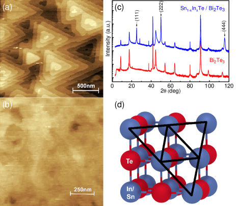
The composition of the grown and annealed films, in particular the concentration of the In dopant , was analyzed by using the energy-dispersive x-ray spectroscopy (EDX) in a scanning electron microscope. Note that the coexistence of the \ceBi2Te3 buffer layer made the determination of the Sn/Te ratio in the \ceSn1-xInxTe layer through the EDX analysis impossible. The crystal structure of the grown films as well as the epitaxial nature of the growth were confirmed by using x-ray diffraction (XRD).
II.2 Device fabrication
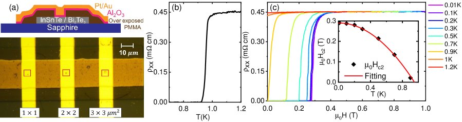
After the growth of Sn1-xInxTe/Bi2Te3 films, photolithography and Ar dry etching were employed to define strips with 20 m width. Then, over-exposed PMMA with small windows written by electron-beam lithography (EBL) was used to cover a part of the strip and define the tunnel-junction area. After using O2 reactive-ion etching and weak Ar etching to clean the surface of the area exposed for tunnel junctions, a thin (0.27 nm) Al2O3 layer was deposited as the tunnel barrier with the atomic layer deposition technique using Ultratec Savannah S200. Finally, the tunnel-junction electrodes were defined with another step of EBL, with sputtering and lift-off of a Pt/Au layer (2 nm/120 nm). Throughout the device fabrication, the samples were never heated to above , so that the properties of the films were not affected by the process.
II.3 Measurements
Transport measurements were performed either in a dry dilution refrigerator (Oxford Instruments Triton 200) with a base temperature of 8 mK or in a helium-3 insert (Oxford Instruments Heliox) in a 14-T superconducting magnet. The ac lock-in technique was used for measuring the resistance and the Hall resistance. In the tunneling spectroscopy experiments, the bias voltage was generated by a Keithley 2450 source meter together with a voltage divider. The tunneling current was measured by a Keithley 2182A nanovoltmeter after amplified by a FEMTO DLCPA-200 current amplifier.
III Results
III.1 Sample characterizations
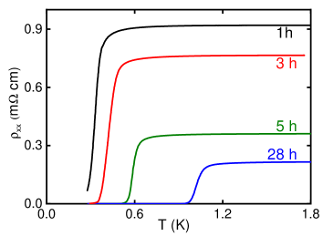
Generally, the \ceSn1-xInxTe films are not superconducting in the as-grown state. The crucial step for successfully obtaining superconducting Sn1-xInxTe films is the in-situ annealing in the MBE chamber immediately after the growth. In our experiments, many samples were grown and annealed under various conditions, resulting in the critical temperature (defined as the mid-point in the resistive transition) ranging from 0.3 to 2.0 K. The depends also on the In content , with the highest observed for 0.12 (see Supplemental Material). The error in is within the last significant digit. Interestingly, the superconducting properties of the films change with the annealing time and temperature, which suggests that some thermal activation process is involved in turning non-superconducting films into superconducting films.
Figure 2 shows the resistive transitions of a series of samples annealed at for different annealing times. The tends to become higher with longer annealing time (a plot of vs annealing time is shown in Supplemental Material for two series of samples). At the same time, although the hole carrier density in the \ceSn1-xInxTe layer of our films cannot be reliably extracted from the Hall resistivity due to the coexisting \ceBi2Te3 layer which contributes electron carriers not , one can infer from the effective Hall carrier density = with the Hall coefficient at low fields] that tends to increase with annealing time.
This observation suggests that the In atoms in as-grown films contribute little to the carrier doping in SnTe and that the annealing promotes the doping of hole carriers. The exact chemistry of the annealing process is beyond the scope of the present work, but we speculate that due to the low growth temperature, In atoms in as-grown films sit at some non-equilibrium positions where they are inactive; after moving to the equilibrium position upon annealing, they become able to provide hole carriers and contribute to the superconductivity. In this regard, it is useful to note that the vapor-transport growth of \ceSn1-xInxTe single crystals in Ref. Novak et al., 2013 was done at , while the present MBE growth was done at . Note also that the of our \ceSn1-xInxTe films are generally lower than that of single crystals with the same values Novak et al. (2013); Zhong et al. (2013), suggesting that some In atoms always remain at non-equilibrium positions.
The structural quality of the as-grown films was checked with atomic force microscopy (AFM) and XRD measurements. Figure 1(a) shows a topographic AFM image of a \ceBi2Te3 film grown with the same conditions as the buffer layer used for the heterostructures. Triangular terraces are clearly visible on the surface of the film, indicating high quality. In Fig. 1(b) one can see that the top surface of the \ceSn1-xInxTe layer is essentially flat without any holes. The XRD pattern taken on a typical \ceSn1-xInxTe/\ceBi2Te3 heterostructure is shown in Fig. 1(c), which demonstrates that only the (LLL) peaks of \ceSn1-xInxTe shows up on top of the \ceBi2Te3 peaks in the data, affirming an epitaxial growth. The lattice constant extracted from the XRD data was 0.63100.0002 nm, which is essentially the same as that of the bulk SnTe (0.632 nm).
The tunnel junctions were fabricated to examine the superconducting properties of \ceSn1-xInxTe. Tunneling spectroscopy probes the density of states (DOS) at the surface, which allows us to infer the energy gap in the SC state. A picture of the device, which is made from a 170-nm-thick = 0.14 film and is reported in the following, is shown in Fig. 3(a). The data of the strip on which the tunnel junctions are made is shown in Fig. 3(b). The observed mid-point of 0.96 K is typical for the films grown in this work. The Hall measurements of this film gave 5 1020 cm-3, which is expected to give a reasonably good approximation of (because the \ceSn1-xInxTe layer was ten times thicker than the \ceBi2Te3 layer) and is comparable to that of superconducting \ceSn1-xInxTe single crystals with 0.04 Novak et al. (2013).
Figure 3(c) shows the magnetic-field dependence of in this device, from which we extract the upper critical field (defined as the mid-point in the resistive transition). From its temperature dependence [Fig. 3(c) inset], we obtain the zero-temperature-limit value, , of 0.28 T, which is in line with the result on single crystals with similar ’s Sasaki et al. (2012). The behavior can be fitted well with the Werthamer-Helfand-Hohenberg (WHH) theory Werthamer et al. (1966) with , suggesting a conventional nature of the bulk superconductivity.
III.2 Tunneling spectroscopy
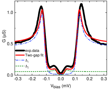
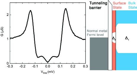
A tunneling spectrum measured at 8 mK in zero field is shown in Fig. 4. Interestingly, this spectrum exhibits two gaps. Given the fact that the parent material SnTe has topological surface states which are preserved after In doping Sato et al. (2013), it is possible that the spectrum reflects the coexistence of bulk and surface superconductivity with different gaps. In fact, the experimental data can be fitted with two individual BCS gaps (blue and green dashed lines) using the following Dynes formula Dynes et al. (1978),
| (1) |
where is the normal-state conductance, is the Fermi function, and is the density of states in the BCS theory given by
| (2) |
Here, is the superconducting gap and is the non-dimensional broadening parameter due to a finite quasi-particle lifetime. By considering two gaps and tuning the parameters of Eqs. (1) and (2), we obtained the red curve in Fig. 4 which describes the observed spectrum reasonably well. The magnitudes of the gaps thus derived are = 0.12000.0003 meV and = 0.03240.0032 meV. It is fair to say that the calculated curve does not match the experimental data perfectly; this may partly be due to the fact that the topological surface states of SnTe on the (111) surface consist of two different kinds of Dirac cones Taskin et al. (2014); Tanaka et al. (2013), which may lead to a total of three different SC gaps.
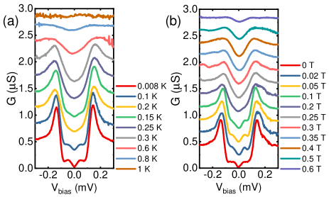
The evolution of the tunneling spectra with temperature and magnetic field is shown in Fig. 5. With increasing temperature from 8 mK [Fig. 5(a)], the smaller gap disappears first at 0.2 K, and then the larger gap vanishes across (= 0.95 K); in the normal state at 1.0 K, the spectrum shows no gap. When the magnetic field is applied perpendicular to the film at 8 mK [Fig. 5(b)], the small-gap feature disappears at 0.2 T, which is below the of 0.28 T at this temperature. Intriguingly, the larger gap remains visible above even in 0.6 T, which suggests that the destruction of superconductivity in magnetic field occurs through the loss of phase coherence.
IV Discussions
Now we discuss the implications of the observed two-gap structure in the tunneling spectra. First, the absence of ZBCP points to the conventional -wave nature of the bulk superconductivity in our \ceSn1-xInxTe thin films. This is reasonable, because it has been discussed that the unconventional odd-parity superconductivity is realized in \ceSn1-xInxTe only when the sample is very clean Novak et al. (2013); in fact, the ZBCP in the point-contact spectroscopy, which is a signature of the surface Andreev boundstates and hence points to unconventional superconductivity, has been observed only in samples with the residual resistivity of 0.15 mcm Sasaki et al. (2012). Given that our thin film used for the tunnel junction device shows the residual resistivity of 0.45 mcm, one would not expect the unconventional bulk SC state to be realized here.
It is also important to notice that SnTe retains its topological surface states even after sufficient In-doping to induce superconductivity, as has been shown by angle-resolved photoemission spectroscopy experiments Sato et al. (2013). It was already discussed for CuxBi2Se3 Hosur et al. (2011) that, when the bulk states become superconducting, Cooper pairing will also occur in the surface states due to the proximity effect. In this case, the corresponding surface SC gap is naturally smaller than that of the bulk. This situation is depicted in Fig. 6. The advantage of this situation is that the bulk states and the surface states coexist in the same material and hence there is no interface barrier to disturb the proximity effect. It is useful to mention that a similar situation has been reported to be realized in the iron-based superconductor \ceFeTe1-xSex Zhang et al. (2018), for which the Majorana bound states have been claimed to be observed in the vortex core Wang et al. (2018).
It is prudent to mention that it was rather difficult to observe the clear two-gap feature in the tunneling spectra, although we have seen it in more than one device. To be specific, we measured a total of 13 junctions, among which 3 showed a clear double gap feature and 6 showed a V-shaped gap suggestive of the two gaps; the other 4 showed the usual U-shaped gap. It appears either that the surface SC gap can be easily smeared due to disorder or that the wave functions of the 2D surface states are much more difficult to be accessed through a tunnel barrier. This in turn supports the surface origin of the small gap and provides evidence against the possibility that \ceSn1-xInxTe is a bulk two-band superconductor and that the smaller gap is associated with a minor bulk band.
From the materials perspective, it is useful to clarify the possible impact of Sn vacancies, because they are the main source of hole doping in pristine SnTe. In this regard, we have extensively studied pristine SnTe films grown on Bi2Te3 buffer layer Taskin et al. (2014), and the typical hole density in pristine SnTe layers grown at (the annealing temperature of this study) was 2 1020 cm-3, which is at the lower border for superconductivity Novak et al. (2013). Since the hole density of our superconducting samples was generally larger (e.g., it was 5 1020 cm-3 in the sample shown in Fig. 3), it would be reasonable to conclude that the Sn vacancies are not playing a dominant role in the occurrence of superconductivity.
One should note that the proximity-induced surface superconductivity in our system is bound to have the effective -wave character, because the four Dirac cones forming the topological surface states are characterized by spin-momentum locking and the resulting pairing is effectively spinless Fu and Kane (2008). An important difference from the case of the topological insulators is that there is more than one Dirac cone; in the case of the (111) surface of SnTe, there is one Dirac cone at the center of the Brillouin zone ( point) plus three additional Dirac cones at the Brillouin zone boundary ( points) Tanaka et al. (2013). It is an interesting future topic to elucidate whether/how the Majorana zero modes associated with such a band structure hybridize when they are created in a vortex core. Also, the effect of uniaxial strain, which will break mirror symmetry and gap out some of the surface Dirac cones, would be interesting to study in this platform.
V Summary
By employing \ceBi2Te3 as a buffer layer, we have been able to grow superconducting \ceSn1-xInxTe epitaxial thin films with the MBE method; however, in-situ annealing of the film for a long time is necessary for observing superconductivity, and is generally lower than that in single crystals. We observed that the hole carrier density inferred from the Hall resistivity tends to increase with longer annealing time, and so is . The residual resistivity of our superconducting films is larger than the cleanest single crystals, which probably causes the bulk SC state to have conventional -wave nature. Nevertheless, our tunneling spectroscopy data strongly suggests that the topological surface states consisting of four Dirac cones are proximitized and obtain a SC gap, which is bound to result in a topological surface superconductivity due to the spin-momentum locking of the surface Dirac cones. It will be important to elucidate the Majorana physics in such a situation with additional valley degrees of freedom.
Acknowledgements.
We thank Fan Yang for his support in the experiments at the initial stage. This project has received funding from the European Research Council (ERC) under the European Union’s Horizon 2020 research and innovation program (Grant Agreement No. 741121) and was also funded by the Deutsche Forschungsgemeinschaft (DFG, German Research Foundation) under CRC 1238 - 277146847 (Subprojects A04 and B01) as well as under Germany’s Excellence Strategy - Cluster of Excellence Matter and Light for Quantum Computing (ML4Q) EXC 2004/1 - 390534769.References
- Qi and Zhang (2011) X.-L. Qi and S.-C. Zhang, Reviews of Modern Physics 83, 1057 (2011).
- Sato and Ando (2017) M. Sato and Y. Ando, Reports on Progress in Physics 80, 076501 (2017).
- Ando (2013) Y. Ando, Journal of the Physical Society of Japan 82, 102001 (2013).
- Wilczek (2009) F. Wilczek, Nature Physics 5, 614 (2009).
- Alicea (2012) J. Alicea, Reports on Progress in Physics 75, 076501 (2012).
- Erickson et al. (2009) A. S. Erickson, J.-H. Chu, M. F. Toney, T. H. Geballe, and I. R. Fisher, Physical Review B 79, 024520 (2009).
- Tanaka et al. (2012) Y. Tanaka, Z. Ren, T. Sato, K. Nakayama, S. Souma, T. Takahashi, K. Segawa, and Y. Ando, Nature Physics 8, 800 (2012).
- Novak et al. (2013) M. Novak, S. Sasaki, M. Kriener, K. Segawa, and Y. Ando, Physical Review B 88, 140502 (2013).
- Sasaki et al. (2012) S. Sasaki, Z. Ren, A. A. Taskin, K. Segawa, L. Fu, and Y. Ando, Physical Review Letters 109, 217004 (2012).
- Maeda et al. (2017) S. Maeda, R. Hirose, K. Matano, M. Novak, Y. Ando, and G.-q. Zheng, Physical Review B 96, 104502 (2017).
- Sato et al. (2013) T. Sato, Y. Tanaka, K. Nakayama, S. Souma, T. Takahashi, S. Sasaki, Z. Ren, A. A. Taskin, K. Segawa, and Y. Ando, Physical Review Letters 110, 206804 (2013).
- Hosur et al. (2011) P. Hosur, P. Ghaemi, R. S. K. Mong, and A. Vishwanath, Physical Review Letters 107, 097001 (2011).
- Fu and Kane (2008) L. Fu and C. L. Kane, Physical Review Letters 100, 096407 (2008).
- Taskin et al. (2014) A. A. Taskin, F. Yang, S. Sasaki, K. Segawa, and Y. Ando, Physical Review B 89, 121302 (2014).
- (15) When a heterostructure gives rise to parallel channels of electron and hole carriers, the Hall effects from the two channels cancel each other and result in a small effective Hall coefficient, which corresponds to an unrealistically large effective carrier density.
- Zhong et al. (2013) R. D. Zhong, J. A. Schneeloch, X. Y. Shi, Z. J. Xu, C. Zhang, J. M. Tranquada, Q. Li, and G. D. Gu, Physical Review B 88, 020505 (2013).
- Werthamer et al. (1966) N. R. Werthamer, E. Helfand, and P. C. Hohenberg, Physical Review 147, 295 (1966).
- Dynes et al. (1978) R. C. Dynes, V. Narayanamurti, and J. P. Garno, Physical Review Letters 41, 1509 (1978).
- Tanaka et al. (2013) Y. Tanaka, T. Shoman, K. Nakayama, S. Souma, T. Sato, T. Takahashi, M. Novak, K. Segawa, and Y. Ando, Physical Review B 88, 235126 (2013).
- Zhang et al. (2018) P. Zhang, K. Yaji, T. Hashimoto, Y. Ota, T. Kondo, K. Okazaki, Z. Wang, J. Wen, G. D. Gu, H. Ding, and S. Shin, Science 360, 182 (2018).
- Wang et al. (2018) D. Wang, L. Kong, P. Fan, H. Chen, S. Zhu, W. Liu, L. Cao, Y. Sun, S. Du, J. Schneeloch, R. Zhong, G. Gu, L. Fu, H. Ding, and H.-J. Gao, Science 362, 333 (2018).