Controlled DC Monitoring of a Superconducting Qubit
Abstract
Creating a transmon qubit using semiconductor-superconductor hybrid materials not only provides electrostatic control of the qubit frequency, it also allows parts of the circuit to be electrically connected and disconnected in situ by operating a semiconductor region of the device as a field-effect transistor (FET). Here, we exploit this feature to compare in the same device characteristics of the qubit, such as frequency and relaxation time, with related transport properties such as critical supercurrent and normal-state resistance. Gradually opening the FET to the monitoring circuit allows the influence of weak-to-strong DC monitoring of a “live” qubit to be measured. A model of this influence yields excellent agreement with experiment, demonstrating a relaxation rate mediated by a gate-controlled environmental coupling.
Josephson junctions (JJs) serve as key elements in a wide range of quantum systems of interest for fundamental explorations and technological applications. JJs, which provide the nonlinearity essential for superconducting qubits Devoret and Schoelkopf (2013), are typically fabricated using insulating tunnel junctions between superconducting metals Paik et al. (2011). Alternative realizations using atomic contacts Bretheau et al. (2013) or superconductor-semiconductor-superconductor (S-Sm-S) junctions Doh et al. (2005); Larsen et al. (2015); de Lange et al. (2015) are receiving growing attention. Hybrid S-Sm-S JJs host a rich spectrum of new phenomena, including a modified current-phase relation (CPR) Golubov et al. (2004); Spanton et al. (2017) different from the sinusoidal CPR of metal-insulator-metal tunnel junctions. Other electrostatically tunable parameters include the sub-gap density of states (DOS), shunt resistance Tinkham (2004), spin-orbit coupling Tosi et al. (2019), and critical current Zuo et al. (2017).
Recent work on S-Sm-S JJs in various platforms relies on either DC (direct current) transport Spanton et al. (2017); Goffman et al. (2017) or cQED (circuit quantum electrodynamics) measurements Kringhøj et al. (2018); Hays et al. (2018); Casparis et al. (2018); Wang et al. (2019). Common to these experiments is that valuable device information is only accessible in one of the two measurement techniques. For instance, measurements estimating individual transmission eigenvalues Riquelme et al. (2005) or measurements probing the local DOS are directly accessible with DC transport but not with cQED. The prospect of combining these techniques potentially allows a deeper understanding of JJ-based quantum systems.
In this Letter, we investigate a modified S-Sm-S JJ design of a gatemon qubit that combines DC transport and coherent cQED qubit measurements. The device is realized in an InAs nanowire with a fully surrounding epitaxial Al shell by removing the Al layer in a second region (besides the JJ itself) allowing that region to function as a field-effect transistor (FET). By switching the FET between being conducting (“on”) or depleted (“off”) using a gate voltage, we are able to implement a controlled transition between the transport and cQED measurement configurations. We demonstrate that the additional tunability does not compromise the quality of the qubit in the cQED configuration, where the FET is off. We further demonstrate control of the qubit relaxation as the FET is turned on, continuously increasing the coupling of the junction to the environment, in agreement with a simple circuit model. Finally, we demonstrate strong correlation between cQED and transport data by comparing the measured qubit frequency spectrum with the switching current directly measured in situ.
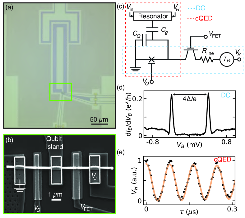
Devices were fabricated on a high resistivity silicon substrate covered with a 20 nm NbTiN film. The nanowire region, qubit-capacitor island, electrostatic gates, on-chip gate-filters, readout resonator, and transmission line were patterned by electron-beam lithography and defined by reactive-ion etching techniques, see Fig. 1(a). The full-shell InAs/Al epitaxial hybrid nanowire is placed at the bottom of the qubit island, see Fig. 1(b) Krogstrup et al. (2015). Two gateable regions are formed by selective wet-etching of the Al in two nm segments defined by electron-beam lithography, aligned with two independent bottom gates, which are separated from the nanowire by a 15 nm thick HfO2 dielectric. The three superconducting segments—ground, qubit island with capacitance , and DC bias —are then contacted with nm sputtered NbTiN, see Fig. 1(b). In this circuit, when the FET is on, DC current/voltage measurements are available [blue box in Fig. 1(c)]. Depleting the FET allows the device to operate as a qubit, where measurements of the heterodyne demodulated transmission allow qubit state determination and allows tuning the qubit frequency over several GHz [red box in Fig. 1(c)].
Setting the voltage on the FET gate to V, which turned the FET fully conducting, and the voltage on the qubit JJ to V makes the voltage drop predominantly across the qubit JJ. In this configuration, the differential conductance dd, probes the convolution of the DOS on each side of the JJ, see Fig. 1(d). Keeping in mind a simple model of JJ spectroscopy Tinkham (2004), we interpret the distance between the two peaks in dd as 4/e = V, where is the induced superconducting gap. In the cQED configuration, with V and V, coherent Rabi oscillations are observed by varying the duration of the qubit drive tone at the qubit frequency GHz. Following the drive tone, a second tone was applied at the readout resonator frequency, GHz, to perform dispersive readout where is measured, see Fig. 1(e). These experiments are carried out in a dilution refrigerator with a base temperature of mK using standard lock-in and DC techniques for the transport measurements and using heterodyne readout and demodulation techniques for the cQED measurements 111See Supplementary Material for additional details on the experimental setup..
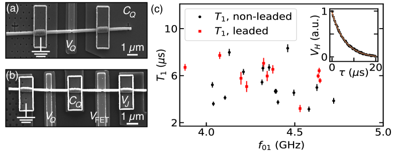
Having demonstrated the ability to probe the qubit JJ with both transport and cQED techniques, we next compare performance to a nominally identical gatemon without the FET and extra DC lead. Scanning electron micrographs of the two devices are shown in Figs. 2(a,b). The measured relaxation time, , is shown for a range of qubit frequencies, , controlled by , in Fig. 2(c). The -measurements were carried out by applying a -pulse, calibrated by a Rabi experiment at , followed by a variable wait time before readout, see Fig. 2(c) inset. Values for were then extracted by fitting to an exponential. We observe no systematic difference between the devices, demonstrating that the addition of a transport lead does not compromise the performance in the cQED configuration.
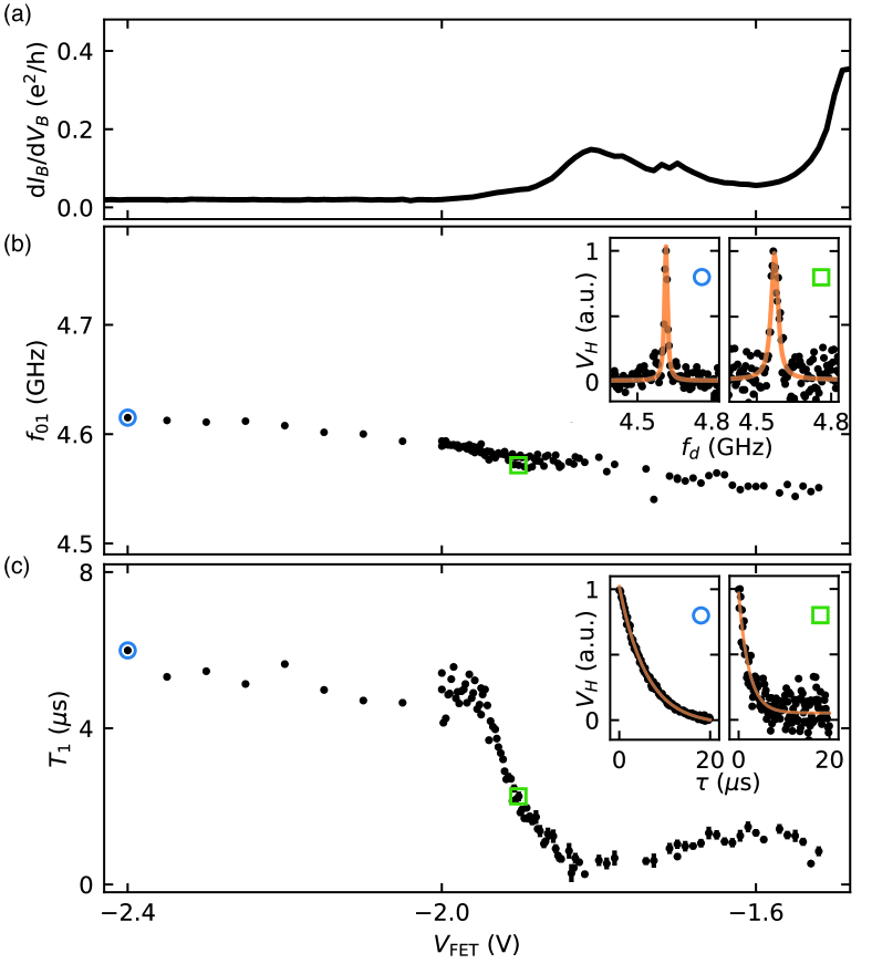
We next monitored dd, and as was varied from off (cQED regime) to on (transport regime). The dd-measurement shown in Fig. 3(a) illustrates how the FET was turned conducting as was increased. Qubit frequency was measured by two-tone spectroscopy, where a drive tone with varying frequency was applied for s, followed by a readout tone at . A Lorentzian fit is used for each value of to extract , see Fig. 3(b) insets. We attribute the weak dependence of on to crosstalk between the two gates.
Following each spectroscopy measurement, a measurement was immediately carried out, see Fig. 3(c), yielding a nearly gate-independent value s for V. At V, we observe a sudden drop in , followed by a short revival at V. We associate the revival in with the corresponding drop in dd observed in Fig. 3(a). For V, and can no longer be resolved, consistent with the increasing dd-values. We note that the dd-curve in Fig. 3(a) was shifted horizontally by a small amount (0.1 V) to align features in dd with corresponding features in . This was done to account for hysteresis in the gate sweep, as the cQED and transport measurements were performed sequentially with a large voltage swing on of V between the two measurements.
We develop a circuit model of qubit relaxation in the leaded device. Within the model, the qubit circuit is coupled through the FET to a series resistance and a parallel capacitance representing an on-chip filter on the lead Mi et al. (2017). The coupling to the environment via the (superconducting) FET junction is modelled as a gate tuneable Josephson inductance , giving a total environment impedance . This impedance can be viewed as a single dissipative element with resistance given by
| (1) |
with admittance Houck et al. (2008). The relaxation rate associated with the lead is given by yielding a total decay rate where is the decay rate associated with relaxation unrelated to the lead.
We estimate Girvin (2014), where is the critical current of the FET, which we in turn relate to the normal-state resistance via the relation Ambegaokar and Baratoff (1963), yielding
| (2) |
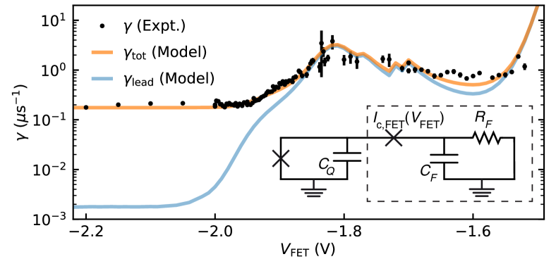
can be found from dd in Fig. 3(a) by subtracting the voltage drop across the line resistance, k, found by fully opening both the qubit JJ and the FET. To associate this value with , we assume no voltage drop across the qubit JJ, justified by , where is the critical current of the qubit JJ. From electrostatic simulations we estimate fF com . We take , where GHz is the average in Fig. 3(b), and eV from Fig. 1(d). Combining Eqs. 1 and 2 with the measured -data, yields the -result in Fig. 4 using and pF as the best fit parameter. We note that electrostatic simulations give pF, in reasonable agreement with the best fit value. We define , where s is the mean value of the at V. Using this estimate for , we calculate the total relaxation time based on the transport data (orange line in Fig. 4) showing excellent agreement with the measured values. The -limit based on the contribution of the lead saturates at ms, indicating that leaded gatemon devices can accommodate large improvements in gatemon relaxation times.
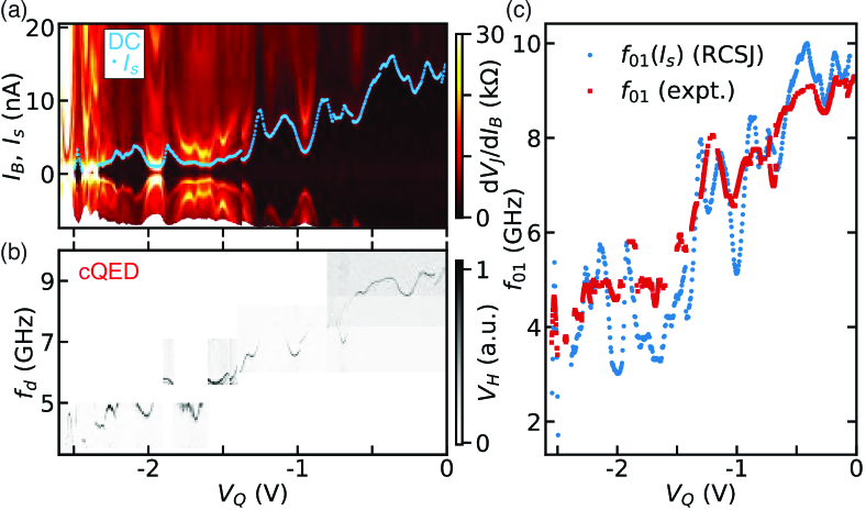
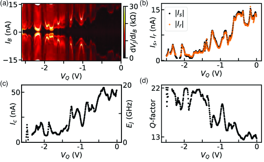
Combining transport and cQED measurements allows for the correlation between critical current and to be observed directly. The critical current is extracted from dd and while sweeping and . We extract the voltage drop and differential resistance across the qubit junction, and dd, by inverting d/d and subtracting . In doing this we assume that there is no voltage drop across the FET junction, since . The qubit resonance is measured over the same range using two-tone spectroscopy, see Fig. 5(b). We note that the two-photon transition to the next harmonic is also observed for some -values, visible at a slightly lower frequency than , given by the anharmonicity.
The relation between the two measurements is shown in Fig. 5(c). In order to estimate we first extract the switching current from the data, taken as the -value at which dd is maximal, while sweeping from negative to positive values [blue dots in Fig. 5(a)]. Bright features at high bias () are likely associated with multiple Andreev reflection (MAR) Klapwijk et al. (1982). To extract from the measured , we model the qubit JJ as an underdamped RCSJ junction with a sinusoidal current-phase relation . Furthermore, we note the small difference between the return current (same definition as at negative ) is slightly smaller than for additional details on the critical current analysis. . In this case, corresponds to the current of equal stability between the resistive and non-resistive state Kautz and Martinis (1990). Under this condition, and for large quality factors, , the ratio depends on quality factor as
| (3) |
where and is the shunt resistance Kautz and Martinis (1990). For simplicity, we take to be equal to the normal state resistance of the junction, . We then apply the Ambegaokar-Baratoff relation Ambegaokar and Baratoff (1963), which allows us to extract by inverting Eq. 3 numerically 222Numerical code and data accompanying the analysis of Fig. 5(c) is found at: https://github.com/anderskringhoej/dc_qubit.. The extracted values of , in turn, yield values for in the range 10-20, consistent with our initial assumptions. For these values of , the RCSJ model takes the electron temperature to be mK to account for the weak asymmetry in and for additional details on the critical current analysis. . Finally, we relate to by using the numerical solution of the standard transmon Hamiltonian, Koch et al. (2007), with and MHz, at the charge degeneracy point with offset charge .
A comparison of the measured and estimated is shown in Fig. 5(c). The model (RCSJ) curve is shifted horizontally by 0.05 V to align the features at V and can be attributed to small gate hysteresis. A clear correlation is observed between the two measurement techniques, especially evident from the matching of local minima and maxima of both spectra and the overall agreement of the absolute values. We attribute the residual quantitative discrepancy to the simplifying assumptions used to determine the shunt resistance of the RCSJ model, which likely do not capture the possible gate dependence of the subgap DOS of the qubit JJ. In addition, the assumption of sinusoidal CPR will break down as the qubit JJ is opened due to increasing mode transmission in the semiconductor junction, leading to small overshoots of the model as perhaps seen around V.
In summary, we have demonstrated the compatibility of DC transport and cQED measurement techniques in gatemon qubits. This method may extend to other material platforms such as two-dimensional electron gases Casparis et al. (2018) or graphene Wang et al. (2019); Kroll et al. (2018). Furthermore, we achieve a controllable relaxation rate potentially relevant for a range of qubit applications such as tunable coupling schemes Chen et al. (2014); Casparis et al. (2019), and controlled qubit relaxation and reset protocols Jones et al. (2013); Ma et al. (2019). In addition, we have demonstrated clear correlation between DC transport and cQED measurements motivating future extensions, such as studying CPRs Spanton et al. (2017) or probing channel transmissions by studying multiple Andreev reflections Goffman et al. (2017) combined with cQED experiments Kringhøj et al. (2018); Hays et al. (2018); Tosi et al. (2019). Combining well-established transport techniques in quantum dot physics with qubit geometries may also be an interesting research direction De Franceschi et al. (2010). Potentially this geometry is also a promising platform to coherently probe Majorana zero modes in cQED measurements Ginossar and Grosfeld (2014), as transport signatures have been demonstrated, both in half-shell nanowires Mourik et al. (2012) and full-shell wires Lutchyn et al. (2018); Vaitiekėnas et al. (2018).
Acknowledgements.
This work was supported by Microsoft and the Danish National Research Foundation. We acknowledge Robert McNeil, Marina Hesselberg, Agnieszka Telecka, Sachin Yadav, Karolis Parfeniukas, Karthik Jambunathan and Shivendra Upadhyay for the device fabrication. We thank Lucas Casparis and Roman Lutchyn for useful discussions, as well as Ruben Grigoryan for input on the electronic setup. BvH would like to thank the Center of Quantum Devices, Niels Bohr Institute for the hospitality during the time in which this study was carried out.References
- Devoret and Schoelkopf (2013) M. H. Devoret and R. J. Schoelkopf, Science 339, 1169 (2013).
- Paik et al. (2011) H. Paik, D. I. Schuster, L. S. Bishop, G. Kirchmair, G. Catelani, A. P. Sears, B. R. Johnson, M. J. Reagor, L. Frunzio, L. I. Glazman, S. M. Girvin, M. H. Devoret, and R. J. Schoelkopf, Phys. Rev. Lett. 107, 240501 (2011).
- Bretheau et al. (2013) L. Bretheau, Ç. Ö. Girit, H. Pothier, D. Esteve, and C. Urbina, Nature 499, 312 (2013).
- Doh et al. (2005) Y.-J. Doh, J. A. van Dam, A. L. Roest, E. P. A. M. Bakkers, L. P. Kouwenhoven, and S. De Franceschi, Science 309, 272 (2005).
- Larsen et al. (2015) T. W. Larsen, K. D. Petersson, F. Kuemmeth, T. S. Jespersen, P. Krogstrup, J. Nygard, and C. M. Marcus, Phys. Rev. Lett. 115, 127001 (2015).
- de Lange et al. (2015) G. de Lange, B. van Heck, A. Bruno, D. J. van Woerkom, A. Geresdi, S. R. Plissard, E. P. A. M. Bakkers, A. R. Akhmerov, and L. DiCarlo, Phys. Rev. Lett. 115, 127002 (2015).
- Golubov et al. (2004) A. A. Golubov, M. Y. Kupriyanov, and E. Il’ichev, Rev. Mod. Phys. 76, 411 (2004).
- Spanton et al. (2017) E. M. Spanton, M. T. Deng, S. Vaitiekėnas, P. Krogstrup, J. Nygård, C. M. Marcus, and K. A. Moler, Nat. Phys. 13, 1177 (2017).
- Tinkham (2004) M. Tinkham, Introduction to superconductivity (Courier Corporation, 2004).
- Tosi et al. (2019) L. Tosi, C. Metzger, M. F. Goffman, C. Urbina, H. Pothier, S. Park, A. L. Yeyati, J. Nygård, and P. Krogstrup, Phys. Rev. X 9, 011010 (2019).
- Zuo et al. (2017) K. Zuo, V. Mourik, D. B. Szombati, B. Nijholt, D. J. van Woerkom, A. Geresdi, J. Chen, V. P. Ostroukh, A. R. Akhmerov, S. R. Plissard, D. Car, E. P. A. M. Bakkers, D. I. Pikulin, L. P. Kouwenhoven, and S. M. Frolov, Phys. Rev. Lett. 119, 187704 (2017).
- Goffman et al. (2017) M. F. Goffman, C. Urbina, H. Pothier, J. Nygård, C. M. Marcus, and P. Krogstrup, New Journal of Physics 19, 092002 (2017).
- Kringhøj et al. (2018) A. Kringhøj, L. Casparis, M. Hell, T. W. Larsen, F. Kuemmeth, M. Leijnse, K. Flensberg, P. Krogstrup, J. Nygård, K. D. Petersson, and C. M. Marcus, Phys. Rev. B 97, 060508 (2018).
- Hays et al. (2018) M. Hays, G. de Lange, K. Serniak, D. J. van Woerkom, D. Bouman, P. Krogstrup, J. Nygård, A. Geresdi, and M. H. Devoret, Phys. Rev. Lett. 121, 047001 (2018).
- Casparis et al. (2018) L. Casparis, M. R. Connolly, M. Kjaergaard, N. J. Pearson, A. Kringhøj, T. W. Larsen, F. Kuemmeth, T. Wang, C. Thomas, S. Gronin, G. C. Gardner, M. J. Manfra, C. M. Marcus, and K. D. Petersson, Nat. Nanotechnol. 13, 915 (2018).
- Wang et al. (2019) J. I.-J. Wang, D. Rodan-Legrain, L. Bretheau, D. L. Campbell, B. Kannan, D. Kim, M. Kjaergaard, P. Krantz, G. O. Samach, et al., Nat. Nanotechnol. 14, 120 (2019).
- Riquelme et al. (2005) J. J. Riquelme, L. de la Vega, A. L. Yeyati, N. Agraït, A. Martin-Rodero, and G. Rubio-Bollinger, Europhysics Letters (EPL) 70, 663 (2005).
- Krogstrup et al. (2015) P. Krogstrup, N. L. B. Ziino, W. Chang, S. M. Albrecht, M. H. Madsen, E. Johnson, J. Nygård, C. M. Marcus, and T. S. Jespersen, Nat. Mater. 14, 400 (2015).
- Note (1) See Supplementary Material for additional details on the experimental setup.
- Mi et al. (2017) X. Mi, J. Cady, D. Zajac, J. Stehlik, L. Edge, and J. R. Petta, Applied Physics Letters 110, 043502 (2017).
- Houck et al. (2008) A. A. Houck, J. A. Schreier, B. R. Johnson, J. M. Chow, J. Koch, J. M. Gambetta, D. I. Schuster, L. Frunzio, M. H. Devoret, S. M. Girvin, and R. J. Schoelkopf, Phys. Rev. Lett. 101, 080502 (2008).
- Girvin (2014) S. M. Girvin, in Quantum Machines: Measurement and Control of Engineered Quantum Systems, Lecture Notes of the Les Houches Summer School: Volume 96, July 2011 (Oxford University Press, 2014).
- Ambegaokar and Baratoff (1963) V. Ambegaokar and A. Baratoff, Phys. Rev. Lett. 11, 104 (1963).
- (24) COMSOL, Inc. [www.comsol.com].
- Klapwijk et al. (1982) T. Klapwijk, G. Blonder, and M. Tinkham, Physica B+ C 109, 1657 (1982).
- (26) See Supplementary Material for additional details on the critical current analysis .
- Kautz and Martinis (1990) R. L. Kautz and J. M. Martinis, Phys. Rev. B 42, 9903 (1990).
- Note (2) Numerical code and data accompanying the analysis of Fig. 5(c) is found at: https://github.com/anderskringhoej/dc_qubit.
- Koch et al. (2007) J. Koch, T. M. Yu, J. M. Gambetta, A. A. Houck, D. I. Schuster, J. Majer, A. Blais, M. H. Devoret, S. M. Girvin, and R. J. Schoelkopf, Phys. Rev. A 76, 042319 (2007).
- Kroll et al. (2018) J. Kroll, W. Uilhoorn, K. van der Enden, D. de Jong, K. Watanabe, T. Taniguchi, S. Goswami, M. Cassidy, and L. Kouwenhoven, Nat. Commun. 9, 4615 (2018).
- Chen et al. (2014) Y. Chen, C. Neill, P. Roushan, N. Leung, M. Fang, R. Barends, J. Kelly, B. Campbell, Z. Chen, B. Chiaro, A. Dunsworth, E. Jeffrey, A. Megrant, J. Y. Mutus, P. J. J. O’Malley, C. M. Quintana, D. Sank, A. Vainsencher, J. Wenner, T. C. White, M. R. Geller, A. N. Cleland, and J. M. Martinis, Phys. Rev. Lett. 113, 220502 (2014).
- Casparis et al. (2019) L. Casparis, N. J. Pearson, A. Kringhøj, T. W. Larsen, F. Kuemmeth, J. Nygård, P. Krogstrup, K. D. Petersson, and C. M. Marcus, Phys. Rev. B 99, 085434 (2019).
- Jones et al. (2013) P. J. Jones, J. A. M. Huhtamäki, J. Salmilehto, K. Y. Tan, and M. Möttönen, Scientific Reports 3, 1987 EP (2013).
- Ma et al. (2019) R. Ma, B. Saxberg, C. Owens, N. Leung, Y. Lu, J. Simon, and D. I. Schuster, Nature 566, 51 (2019).
- De Franceschi et al. (2010) S. De Franceschi, L. Kouwenhoven, C. Schönenberger, and W. Wernsdorfer, Nat. Nanotechnol. 5, 703 (2010).
- Ginossar and Grosfeld (2014) E. Ginossar and E. Grosfeld, Nat. Commun. 5, 4772 EP (2014).
- Mourik et al. (2012) V. Mourik, K. Zuo, S. M. Frolov, S. R. Plissard, E. P. A. M. Bakkers, and L. P. Kouwenhoven, Science 336, 1003 (2012).
- Lutchyn et al. (2018) R. M. Lutchyn, G. W. Winkler, B. Van Heck, T. Karzig, K. Flensberg, L. I. Glazman, and C. Nayak, arXiv preprint arXiv:1809.05512 (2018).
- Vaitiekėnas et al. (2018) S. Vaitiekėnas, M.-T. Deng, P. Krogstrup, and C. M. Marcus, arXiv preprint arXiv:1809.05513 (2018).
I Supplementary Material
I.1 Experimental setup
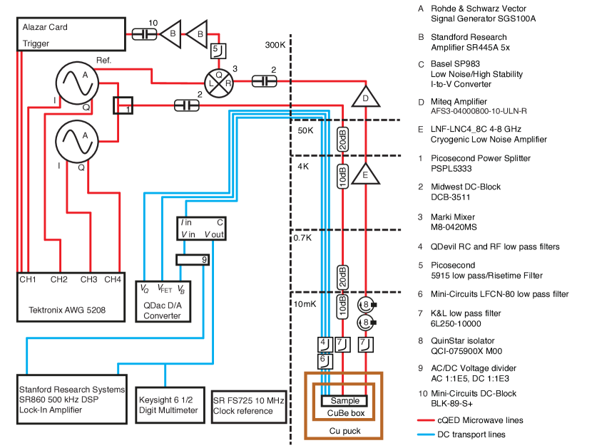
The measurements presented in the paper are conducted in a cryogen-free dilution refrigerator with a base temperature of mK. A detailed schematic of the electronic setup is shown in Fig. S1. The sample is mounted to a Cu circuit board located in a indium sealed CuBe box mounted inside another Cu box, which is thermally attached to the mixing chamber plate. DC lines (blue lines in Fig. S1) connect to the sample through a loom heavily filtered at frequencies above 80 MHz via both the QDevil and the LFCN-80 low pass filters. For transport measurements we measure a small AC current using the SR860 lock-in amplifier while also measuring the DC current to ground with the Keysight multimeter. Both current signals are amplified and converted to a voltage by the Basel SP983 I-to-V converter.
Two microwave coaxial drive lines connect to the sample (red lines in Fig. S1). The combined input signal is generated by two RF sources and is heavily attenuated and filtered above 10 GHz with a KL low pass filter. These two signals are used for qubit drive and readout drive, respectively. The output signal is again filtered and amplified at the 4 K stage with a cryogenic low noise amplifier with a bandwidth of 4–8 GHz with further amplification at room temperature using the Miteq amplifier. The output signal is down converted to an intermediate frequency by mixing with a local oscillator and filtering of the high frequency component. After another amplification stage using the SR445A amplifier, the intermediate frequency signal is digitized and digitally down converted in order to extract the in-phase and quadrature components of the readout signal.
The SR FS725 10 MHz clock reference is connected to the Alazar card, signal generators and the AWG for synchronisation of the microwave signals.
I.2 RCSJ modelling details and data
To supplement the data and the analysis presented in Fig. 5, we measured dd as a function of and for a -range where we were able to extract both and for the entire -range, see Fig. S2(a). This dataset shows quantitatively almost the same features as the dataset in the main text. However, due to a larger amount of drift, possibly due to longer acquisition time, we use the dataset in Fig. 5(a) to perform the modelling in the main text. From the measurement shown in Fig. S2(a) we are able to extract both and , see Fig. S2(b). Here we observe a weak asymmetry between and for the full -range, which justifies the use of the RCSJ model applied in the analysis of Fig. 5(c).
In addition, we compute the extracted critical current and used in our RCSJ analysis, as shown in Fig. S2(c). Based on these -values we estimate the electron temperature to be 50mK, such that the -ratios account for the weak asymmetry between and Kautz and Martinis (1990). To further justify the application of the limit, we numerically extract the -values, as shown in Fig. S2(d).