Influence of Edge Functionalization on Electronic and Optical Properties of Armchair Phosphorene Nanoribbons: a First-Principles Study
Abstract
In this work, we present a systematic first-principles density-functional theory based study of geometry, electronic structure, and optical properties of armchair phosphorene nanoribbons (APNRs), with the aim of understanding the influence of edge passivation. Ribbons of width ranging from 0.33 nm to 3.8 nm were considered, with their edges functionalized with the groups H, OH, F, Cl, S, and Se. The geometries of various APNRs were optimized, and the stability was checked by calculating their formation energies. Using the relaxed geometries, calculations of their band structure and optical properties were performed. Pristine APNRs, as expected, exhibit significant edge reconstruction, rendering them indirect band gap semiconductors, except for one width (, where is the width parameter) for which a direct band gap is observed. The edge passivated APNRs are found to be direct band gap semiconductors, with the band gap at the -point, for all the functional groups considered in this work. To obtain accurate estimates of band gaps, calculations were also performed using HSE06 hybrid functional for several APNRs. Our calculations reveal that functional groups have significant influence on the band gaps and optical properties of narrower APNRs. For wider passivated ribbons, with the increasing ribbon widths, the gaps converge to almost the same value, irrespective of the group. We also performed calculations including the spin-orbit coupling (SOC) for hydrogen passivated APNRs with and 11. We found that SOC has no significant influence on the band structure of the studied APNRs. However, for the broader APNR, a lowering of peak intensities was observed in the optical absorption spectrum beyond 5 eV.
I Introduction
For the past few decades, there has been tremendous amount of interest in reduced-dimensional systems, in general, and two-dimensional (2D) materials, in particular.(Cui et al., 2018; Carvalho et al., 2016; Qiu et al., 2018; Batmunkh et al., 2016; Geng and Yang, 2018) Not only are 2D materials interesting from the basic science point of view, they also offer easier tuning of their electronic properties, as compared to their bulk counterparts. The tailoring of their electronic properties is crucial to make them suitable for applications in electronics and optics. Phosphorene not only has a finite direct band gap, but also has high carrier mobility, and in-plane anisotropy. This 2D-material offers many potential applications not only in transport-based electronic and spintronic devices, but also in sensors, information storage, and optoelectronic devices.(Akhtar et al., 2017) After the successful exfoliation of phosphorene from bulk black phosphorus,(Li et al., 2014a; Liu et al., 2014; Woomer et al., 2015; Brent et al., 2014; Zhinan et al., 2015; Adriano et al., 2017) it has been a subject of extensive experimental as well as theoretical research.(Liu et al., 2014; Li et al., 2014b; Koenig et al., 2014; Dai and Zeng, 2014; Zhu et al., 2015, 2016) The band gap of phosphorene can be further tailored by manipulating the number of layers, in-layer strain,(Liu et al., 2014) forming heterostructures such as nanoribbons and quantum dots, as well as by chemical means such as edge passivation.
In this work, we present a systematic first-principles density functional theory (DFT) based study of the geometry, electronic structure, and optical properties of armchair-type phosphorene nanoribbons (APNRs), with the aim of understanding the influence of edge-passivation on them. Numerous theoretical studies of phosphorene and its heterostructures have been performed over last few years, therefore, it is difficult to cite all of them. However, below we review the most relevant theoretical studies of the electronic structure and related properties of APNRs, which have been studied mainly using two methodologies: (a) semi-empirical tight-binding model, and (b) first-principles DFT.
Using the tight-binding model Sisakht and coworkers(Taghizadeh Sisakht et al., 2015) studied the scaling laws in phosphorene nanoribbons (PNRs), Soleimanikahnoj and Knezevic(Soleimanikahnoj and Knezevic, 2017) and Forte et al.(Forte et al., 2019) studied the effect of vertical electric field on electronic and transport properties of multilayer APNRs , while Yuan and Cheng(Yuan and Cheng, 2017) investigated the influence of strain on the transport properties of APNRs.
Guo et al.(Guo et al., 2014) studied the electronic structure and geometries of bare and H-passivated APNRs using a first-principles DFT based approach. Using the DFT(Tran and Yang, 2014) Tran and Yang studied the electronic structure and optical absorption of H-passivated APNRs, and also reported scaling laws for their band gaps. Carvalho and coworkers(Carvalho et al., 2014) computed the formation energies of APNRs, and also examined the edge-induced gap states in them, employing DFT and analytical models. The influence of edge-passivation by chemical groups such as H, F, Cl, O, S, Se, and OH, on the electronic properties of APNRs was studied by Peng et al.(Peng et al., 2014), using the DFT. Maity and coworkers(Maity et al., 2014) studied edge reconstruction and Peierls transition in PNRs, using a DFT based approach. Wu et al.(Wu et al., 2015) computed the electronic and transport properties of H-passivated APNRs using a methodology combining DFT and nonequilibrium Green’s functions (NEGF.). The electronic structure and the Seeback coefficients of H-passivated PNRs, with possible thermo-electric applications, were studied by Zhang et al.(Zhang et al., 2014) also using the first-principles DFT. Hu, Lin, and Yang(Hu et al., 2015) studied the edge reconstruction in unpassivated PNRs, including a few thousands to ten thousand atoms in their calculations, by means of Discontinuous Galerkin DFT (DGDFT) methodology. The optical properties of relatively narrow APNRs were studied by Nourbakhsh and Asgari(Nourbakhsh and Asgari, 2016) , by going beyond the first-principles DFT approach, by including electron-correlation and particle-hole effects within G0W0 and Bethe-Salpeter equation (BSE) methodology. including excitonic effects. Shekarforoush, Shiri and Khoeini(Shekarforoush et al., 2018) computed the linear and non-linear optical properties of H-passivated APNRs of moderate widths, using first-principles DFT. Kaur et al.(Kaur et al., 2018) also employed the first-principles DFT to study the electronic, structural, and mechanical properties of PNRs of several allotropes of phosphorene. Electronic structure of pristine and APNRs passivated by H, O, and OH wwas studied by Ding and coworkers(Ding et al., 2016) using first-principles DFT. Possibility of using bilayer PNRs as pressure sensors was explored by Lv et al.(Lv et al., 2017) theoretically, using the first-principles DFT. Li and coworkers(Li et al., 2014c) also studied the electronic structure of both pristine and H-passivated PNRs of moderate widths, using the first-principles DFT. Using a similar computational approach, Gueorguiev and coworkers have studied other lower-dimensional systems, such as bismuth sheets, and carbon chains.(dos Santos et al., 2011; Freitas et al., 2016)
In this work, we have studied both the pristine and the passivated APNRs ranging from very narrow ribbons of width 0.32 nm to very broad ones of width 3.85 nm, using the PBE functional. The widths of nanoribbons can also be denoted using an integer parameter (see Fig. 1(a)), in terms of which the APNRs studied in this work are in the range . The novel aspects of this work are: (a) the maximum width of ribbons studied in this work is more than the earlier first-princples DFT based studies, such as H-passivated APNRs of maximum width 2.50 nm by Tran et al.(Tran and Yang, 2014), and pristine and passivated APNRs by Peng et al.(Peng et al., 2014), on selective widths up to 3.50 nm, (b) narrow pristine APNRs of widths have been studied, for which no earlier work has been reported, (c) the optical absorption spectra of pristine and all edge-passivated APNRs, whereas the earlier calculations employing the same approach exist only for H-passivated ribbons,(Tran and Yang, 2014) (d) the bands involved in the transitions leading to a few important peaks in the absorption spectrum have been identified, (e) for obtaining more accurate estimates of the band gaps, we also performed the band structure calculations using the HSE06 hybrid functional for ribbons of medium width, with several passivating groups, whereas earlier calculations were performed only for -H, and -OH passivated ribbons.(Ding et al., 2016) Additionally, we also analyzed the calculated data of formation energies and concluded that: (i) the smaller ribbons are more stable than the wider APNRs, (ii) F- and OH-saturated structures are comparatively much more stable, as compared to the H-passivated ones. Furthermore, we also performed a detailed analysis of the contributions of various atoms to the the orbitals in the frontier regions of valence and conduction bands. To the best of our knowledge, none of the previous works has presented calculations on electronic and optical properties of APNRs over such a large range of width, for a variety of passivating groups.
II Theoretical approach and Computational details
The nanoribbons investigated in this work were taken to be periodic along the -direction, with at least 15 Å vacuum included in the supercell along both the - and - directions to minimize the spurious interactions. First, geometry optimization for each ribbon was performed, followed by the calculations of quantities such as formation energies, the band gaps, the band structure, and the optical absorption spectra. The calculations were carried out by employing the first principles ab initio comprehensive density functional theory (DFT),(Kohn and Sham, 1965) as implemented in the computer program Vienna Ab-initio Simulation Package (VASP).(Kresse and Furthmüller, 1996a, b) For the purpose, we used projector-augmented wave (PAW) pseudo-potentials(Blöchl, 1994; Kresse and Joubert, 1999) and Perdew-Burke-Ernzerhof (PBE) exchange-correlation functional(Perdew et al., 1996) for geometry optimization.
The kinetic energy cut-off of 500 eV was used for the plain wave basis set. For geometry optimization, a k-point grid of 1141 were chosen in the reciprocal space by employing Monkhorst-Pack centered at the point. During geometry optimization, the convergence cutoff for the electronic energy was eV, while that for Hellmann-Feynman force was set to eV/Å. For subsequent total energy and density of states calculations, a tighter energy cutoff of eV, along with a denser k-mesh grid of 1451, were employed. For band structure calculations of the optimized APNRs, 100 k-points were included for the path from to Y. Both the PBE and Heyd-Scuseria-Ernzerhof (HSE06)(Heyd et al., 2003a) hybrid functionals ware employed for self-consistent electronic structure calculations.
III Results and Discussion
In this section we present and discuss the results of our calculations on the geometry, stability, electronic structure, and optical properties of APNRs, with edges passivated by different functional groups.
III.1 Geometry
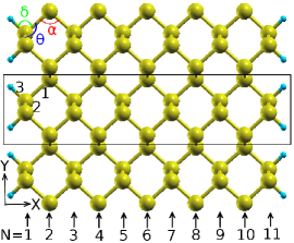
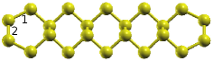
Henceforth, we denote a given ribbon by its width (see Fig. 1(a)), thus an APNR of width will be denoted as -APNR. Additionally, edge bond angles and bond lengths relevant for both passivated and pristine nanoribbons are also defined in Fig. 1. We performed geometry optimization for -APNRs, with , for all functional groups except OH and F, for which we performed calculations only for . Optimized geometries for all functional groups as well for the pristine case are presented in Table 1, for . Using the same methodology we performed geometry optimization on phosphorene monolayer for reference, and the corresponding relaxed geometry parameters are also presented in Table 1. We note that our optimized geometries both for APNRs and phosphorene monolayer are in excellent agreement with results reported by Peng et al.(Peng et al., 2014), also based upon first-principles DFT.
For the pristine APNRs, the P-P bond length, l2 has been reduced significantly as compared to the other structures in order to stabilize the dangling bonds at the edges, and, because of that, the bond angles and have also increased considerably. Generally, one observes the tendency that larger the edge passivating atom/group, the longer the corresponding bond length. In the present case also the tendency holds true in that when selenium (Se) passivates the edge, l3 is the longest as compared to its values for other edge atoms. As far as interior bond lengths and angles are concerned, they differ from their edge counterparts by small amounts.

| Structure | l1 | l2 | l3 | |||||||||
|---|---|---|---|---|---|---|---|---|---|---|---|---|
| (Å) | (Å) | (Å) | (∘) | (∘) | (∘) | |||||||
| Mono-layer | 2.22 | 2.26 | NA | 95.9 | 104.1 | NA | ||||||
| Pristine | 2.23 | 2.07 | NA | 110.8 | 119.4 | NA | ||||||
| H | 2.22 | 2.25 | 1.44 | 95.9 | 103.3 | 93.0 | ||||||
| OH | 2.25 | 2.26 | 1.64 | 96.9 | 99.9 | 103.2 | ||||||
| F | 2.23 | 2.25 | 1.64 | 94.7 | 97.8 | 98.6 | ||||||
| Cl | 2.24 | 2.26 | 2.07 | 92.1 | 96.1 | 101.7 | ||||||
| S | 2.23 | 2.25 | 2.12 | 97.1 | 104.9 | 99.5 | ||||||
| Se | 2.23 | 2.24 | 2.28 | 95.3 | 102.9 | 100.0 |
III.2 Formation energy and relative stability
To quantify the energetic stability of an APNR, we define its formation energy () as follows
| (1) |
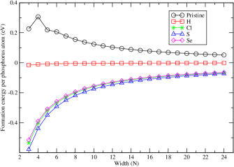
where and , respectively, are the formation energy and total energy of a pure or edge-passivated APNR within a super-cell containing phosphorus atoms, and passivation atoms/groups at the edge. Furthermore, is the energy per phosphorus atom of an infinite phosphorene sheet, and is the energy of a edge-passivating foreign atom which we calculated as . For the case of edge passivation by OH group, we used . Thus, the formation energy measures energetic stability of an edge-passivated APNR, with respect to an infinite phosphorene sheet. Negative value of clearly implies that the formation of a given APNR from phosphorene sheet is energetically possible. In our calculations, =4 for all APNRs considered in this work (see Fig. 1), while depends on the width of the nanoribbon. For example, for 11-APNR, =22. Energies of all the molecules considered as functional group are presented in the Table S1 of the supporting information. In the pristine case, the third term on the right hand side of Eq. 1 is absent. In Fig. 2a, we present the plot of the width dependence of the formation energy per phophorus (P) atom ( for all the pristine and edge-saturated APNR structures considered in this work, while the formation energies of pristine as well as edge-passivated 11-APNRs are plotted in Fig. 2b. The following trends emerge from these figures: (a) with positive values of , pristine APNRs are energetically unstable, however, their values of are decreasing with the width, i.e., they are reaching the limit of infinite sheet, (b) for H-passivated ribbons, the formation energies are negative, but much smaller than those for APNRs passivated by other groups, (c) for all edge-passivated APNRs, the formation energy per P-atom is gradulally increasing with the ribbon-width, and saturating for larger widths, implying that the narrower saturated ribbons are more stable than the broader ones. For the specific case of 11-APNR (see Fig. 2b), we note that the F-passivated APNR is most stable, closely followed by the OH passivated ribbon. These results of ours are consistent with those reported by Ding et al.(Ding et al., 2016).

III.3 Band gaps
In this section we discuss the band gaps of APNRs as functions of their width, and edge-passivating groups.
| Passivating | |||||||
|---|---|---|---|---|---|---|---|
| Atom | 3 | 4 | 5 | 6 | 7 | 8 | 9 |
| H | 1.97 | 1.53 | 1.30 | 1.19 | 1.10 | 1.05 | 1.02 |
| Cl | 1.66 | 1.28 | 1.29 | 1.22 | 1.09 | 1.04 | 1.04 |
| S | 1.28 | 1.25 | 1.18 | 1.10 | 1.04 | 1.03 | 1.01 |
| Se | 1.17 | 1.16 | 1.07 | 0.99 | 0.95 | 0.96 | 0.95 |
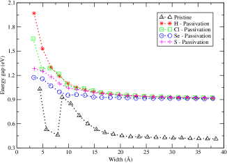
In Fig.3, we present the band gaps of APNRs as functions of their widths, and our results are in good agreement with those reported in earlier studies.(Peng et al., 2014; Tran and Yang, 2014) An examination of the figure reveals the following general trends: (a) with the increasing width, the band gaps show a decreasing trend approaching saturation around 2.5 nm, (b) for a given width, the band gap of a pristine nanoribbon is smaller than that of a passivated one, and the difference grows with the increasing width, before eventually saturating, (c) for a given width, H-passivated ribbons have the largest band gaps, while those passivated with Se have the smallest. But for the pristine ribbons a peculiar behavior is observed in that the band gaps do not exhibit a monotonic decrease with increasing width, for narrower ribbons. At first, the band-gap decreases and reaches close to the final saturation value, then suddenly increases again, eventually exhibiting a normal decreasing trend with respect to the width. and follows the regular trend. This is mainly due to the huge distortion in the smaller structures to stabilize the dangling bonds which make changes in the symmetry of wave function of the edge states. To the best of our knowledge, so far there is no literature on on the electronic structure of pristine APNRs, with widths in the range .
It is also instructive to compare our obtained band gaps with that of infinite phosphorene monolayer. Using the PBE functional, and the geometry parameters listed in Table 1, for the monolayer phosphorene we obtained the band gap to be 0.91 eV. This compares well with our saturated values of 0.92 eV for the H-passivated APNRs, and 0.91 for the selenium passivated ribbons. However, it is significantly larger than the saturated band gap value of 0.40 eV obtained for the pristine APNRs, thereby implying that pristine APNRs, due to their distorted edges, do not correctly evolve into monolayer phosphorene, with the increasing width. To examine the effect of spin-orbit coupling, we carried out calculations for hydrogen saturated 5- and 11-APNRs, but no significant changes were observed.
| Structure | Band-gap (eV) | Band-gap | |||||
|---|---|---|---|---|---|---|---|
|
type | ||||||
| Pristine |
|
Indirect | |||||
| H |
|
direct | |||||
| OH |
|
direct | |||||
| F |
|
direct | |||||
| Cl |
|
direct | |||||
| S |
|
direct | |||||
| Se |
|
direct |
It is well-known that DFT-PBE based approaches generally underestimate the bang gaps significantly, therefore, one can wonder as to how reliable are our PBE functional based calculations, both quantitatively, and qualitatively. To verify that, we performed band gap calculations on 11-APNRs for pristine as well as various edge-passivated configurations using the HSE06 functional, and the results are presented in Table 3, along with the corresponding values obtained using the PBE functional. HSE06 functional belongs to the class of hybrid functionals,(Heyd et al., 2003b; Schimka et al., 2011) whose predicted band gap values are normally fairly accurate, and compare well with the experiments.(Pela et al., 2015; Garza and Scuseria, 2016) We note the following: (a) HSE06 band gap values for all the cases are significantly higher as compared to the PBE values, and (b) the trends in the band gap values ranging from pristine ribbons to the ones passivated by Se atom are similar for both the HSE06 and PBE calculations. Therefore, we conclude that although PBE functional significantly underestimates the band gaps, however it reproduces the qualitative features of the behavior of band gaps with respect to the passivation groups. Based upon these results, and the data presented in Fig. 3 and Table 2, we can say with certainty that for the narrower APNRs, band gaps depend very sensitively on the nature of edge passivation; those passivated by H atoms have the largest gaps, while Se passivated ones have the smallest gaps. This information can be used to tune the electronic and optical properties of APNRs.
III.4 Band structure and density of states (DOS)
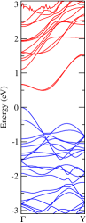
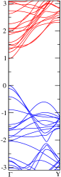
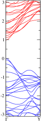
The computed band structures of pristine as well as passivated 11-APNR are shown in the Fig. 5. Our calculations reveal that the band gaps of pristine APNRs of all but one width are indirect, with the valence band maximum (VBM) at point, and the conduction band minimum (CBM) between the and Y points. The only exception to this is 5-APNR which, as shown in Fig. 4, is a semiconductor with a direct band gap of about 0.46 eV, at the point. To the best of our knowledge, the band structure of pristine 5-APNR has not been discussed in the literature earlier, and the reasons behind its direct band gap could lie in its geometry, presented in Fig. S1 of the Supporting Information. The bond lengths l1 and l2 of 5-APNR are 2.30 Å and 2.29 Å, respectively, which are elongated with respect to the wider pristine structures. As far as bond angles are concerned, the calculated value of is 121.4, which is larger as compared to wider APNRs, while the value of at 110∘ is smaller as compared to the wider ribbons.
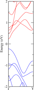
The passivated nanoribbons, irrespective of their width, or the nature of the passivating groups, turn out to be direct band gap semiconductors, with the VBMs and CBMs located at the high symmetry point. This is obvious from the Fig. 5, which contains the band structures of 11-APNRs passivated by H, OH, F, Cl, S, and Se. These results of ours are in very good qualitative and quantitative agreement with the calculations of Peng et al.(Peng et al., 2014) and Tran and Yang(Tran and Yang, 2014). We performed calculations including the spin-orbit coupling for hydrogen passivated 5- and 11-APNRs, and observed no significant changes in the band structures.
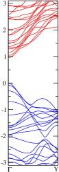
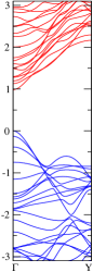
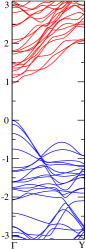
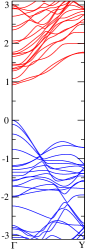
For the edge-passivated APNRs, we find that both the VBM and the CBM derive predominant contributions from p-type orbitals of P atoms located both on the edges, as well as the interior of the ribbons. However, for the Se-passivated APNRs, the lowest conduction band, including the CBM, is mainly composed of the p-type orbitals located on the Se atoms. As far as deeper valence band orbitals are concerned, they derive dominant contribution from the s-type orbitals of the P atoms. The contributions of passivating atoms to two lowest conduction bands increase with the increasing atom sizes, being negligible for H-passivated ribbons, and eventually reaching maximum values for Se-passivated APNRs. A possible reason behind this behavior is that the electron clouds of larger passivating atoms are extended further into the interior of the nanoribbon, allowing its hybridization with the lower conduction bands leading to their lowering, thus causing a reduction in the band gaps.
We have compared the band structure of H-passivated 11-APNR computed using the HSE06 functional, with that obtained from the PBE functional, in Fig. S4 of the Supporting Information. The HSE06 band structure calculations were initiated using the PBE wave functions, and from the figure it is obvious that the HSE bands close to the Fermi level are similar to the PBE ones, except undergoing a rigid shift resulting from the widening of the band gap. Similar trends were also observed in the HSE band structures of APNRs passivated by other groups.
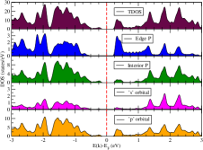
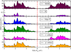
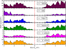
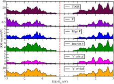
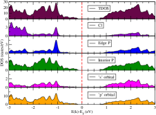
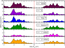
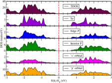
The total, orbital projected, and atom projected density of states (DOS) for the case of 11-APNRs are presented in Fig. 6. For the pristine ribbon, we note that the edge P atoms contribute more to the conduction band states near the Fermi level, as compared to the interior P atoms; while for the valence bands, both the interior as well edge atoms make significant contributions. For the passivated APNRs, we see that both the edge and the interior P atoms make significant contributions to the frontier bands. Furthermore, increasing contribution of the passivating atoms to the bands near the Fermi level, with their increasing sizes is also obvious from various DOS plots. It is also clear from these plots that the p-type orbitals contribute more than the s-type orbitals to the frontier states.
III.5 Optical absorption spectra
Based upon the single-particle DFT-PBE level band structure calculations, we computed the optical absorption spectra of pristine, as well as edge-saturated N-APNRs with various functional groups, for N=3–24, with the incident light polarized along the length of the ribbons. The spectrum was calculated according to the standard formalism, by computing the imaginary part of the dielectric constant matrix, as implemented in the VASP program.(Kresse and Furthmüller, 1996a, b)
In Fig. 7 we present the calculated optical absorption spectra of pristine and edge-passivated 11-APNRs. To the best of our knowledge, the only previous calculation of the absorption spectrum of APNRs, based upon the first-principles DFT methodology, was reported by Tran et al.(Tran and Yang, 2014), for H-passivated ribbons, but only up to 2.4 eV. Here we report calculations not just on H-passivated APNRs, but also on pristine ribbons, and also those passivated by other groups. In Fig. S3 of Supporting Information, we also present the results of similar calculations on narrower 5-APNRs, and broader 24-APNRs.
To investigate the effects of spin-orbit coupling (SOC) on the absorption spectra of APNRs, we carried out calculations for hydrogen passivated 5- and 11-APNRs, and in Fig. S6 of the Supporting Information, we compare the spectra computed with and without SOC. For the narrower ribbon, i.e., 5-APNR, no significant change in peak locations as well as intensity was observed. But, for the broader ribbon, i.e., 11-APNR, although no noticeable change in the peak locations is seen, but the peak intensities do get weaker for energies beyond 5 eV.
In order to benchmark the calculated spectra, in Table 4 we compare the locations of our absorption peaks, with those reported by Tran et al.(Tran and Yang, 2014), for H-passivated ribbons. Because Tran et al.(Tran and Yang, 2014) reported the spectra only up to 2.4 eV, therefore, for N=3 and N=5, we are able to compare only one peak each, while for N=10, comparison for three peaks is possible (see Table 4). We note that the our peak locations are about 0.1 eV blue shifted as compared to the ones reported by Tran et al.(Tran and Yang, 2014), which is a fairly good agreement given the fact that they employed a different computer code, Quantum Espresso(Giannozzi et al., 2009), for their calculations.
| N | This work | Tran et al.(Ref.(Tran and Yang, 2014)) | ||||||||
|---|---|---|---|---|---|---|---|---|---|---|
| 3 | 2.05 | 1.93 | ||||||||
| 5 | 1.37 | 1.25 | ||||||||
| 10 |
|
|
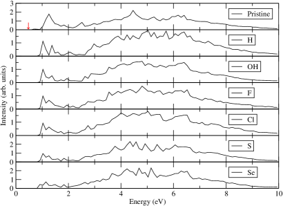
On examining the absorption spectra of 11-APNRs in Fig. 7, we see the following trends: (a) for the pristine ribbon there is no peak at the location of its band gap, consistent with the fact that it is an indirect band gap semiconductor, (b) for all the passivated ribbons, as expected, the first peak occurs at the location of the band gap, and (c) for all the APNRs, the highest intensity peak occurs at energies larger than 4 eV.
We present the locations of the first, the second, and the most intense peaks of optical absorption spectra of pristine and passivated 11-APNRs in the Table 5. We also investigated the orbitals involved in the one-electron transitions leading to these peaks, and they are also presented in the same Table, in parentheses next to the peak energies. We note that for the pristine APNR, the first peak occurs at 0.69 eV, caused by the orbital transition , for a nonzero momentum value, very close to the point. For all the passivated APNRs, the first peak appears due to the transition, occurring at the point. The second peak for the pristine ribbon is due to the transition , slightly away from the point. For APNRs passivated by monovalent groups, namely, H, OH, F and Cl, transition gives rise to the second peak, while the same peak for the divalent passivating groups S and Se, is due to transitions , and , respectively. In all the cases, these optical transitions occur either at the point, or fairly close to it. Finally, we examine the nature of the highest intensity peaks located at higher energies. Quite expectedly, the corresponding transitions involves bands far away from the Fermi level (see Table 5), and they occur closer to the edge of the Brillouin zone, as shown for the case of H-saturated 11-APNR, in Fig. S2 of the Supporting Information.
| Saturation | First peak | Second peak | Most intense peak |
|---|---|---|---|
| position (eV) | position (eV) | position (eV) | |
| Pristine | 0.69 () | 1.26 () | 4.46 () |
| H | 1.03 () | 1.38 () | 5.04 () |
| OH | 1.03 () | 1.38 () | 4.81 () |
| F | 1.03 () | 1.28 () | 4.82 () |
| Cl | 1.03 () | 1.27 () | 5.05 () |
| S | 1.03 () | 1.27 () | 4.35 () |
| Se | 0.92 () | 1.14 () | 5.16 () |
At this point, one may wonder as to how close are the absorption spectra of our widest system 24-APNR to that of the infinite phosphorene monolayer. To investigate that, in Fig. S5 of the Supporting Information, we compare the optical absorption spectra of H-passivated 24-APNR to that of monolayer phosphorene, both computed using the DFT-PBE approach. From the figure it is obvious that the two spectra are very similar to each other in terms of intensity profile, as well as peak locations, except that the monolayer spectrum, quite expectedly, is much more intense. Thus, for all practical purposes we can assume that the optical properties of 24-APNR have saturated to the monolayer value.
When we compare the absorption spectra of 11-APNRs with those of 5-APNRs and 24-APNRs (see Fig. S3, Supporting Information) we note that for the pristine 5-APNR, the first absorption peak is at the band gap, because it is a direct band gap material. For the passivated nanoribbons, we note that the basic qualitative features of the absorption spectra are the same irrespective of the widths. For narrower ribbons the absorption peaks are sharper and well separated, while for broader ones they evolve into absorption bands.
We also note that the qualitative features of the absorption spectrum of H-passivated 5-APNR computed using the GW+BSE approach(Nourbakhsh and Asgari, 2016) are quite similar to that computed by us using the PBE-DFT approach, except, of course, for the peak locations.
IV Conclusions
In this work, we presented results on first-principles DFT calculations on pristine and passivated -APNRs, ranging from the very narrow (), to the very broad (). We first performed geometry optimization for each ribbon, and for those geometries computed quantities such as the formation energies, the band gaps, the band structure, and the optical absorption spectra, using the PBE functional. In addition, for a selected few ribbons, we also calculated the band gaps using the HSE06 functional, and found that it yields band gaps significantly larger than those predicted by PBE-functional based calculations. This implies that electron correlations make important contributions, highlighting their importance in the reduced dimensional systems such as APNRs. Therefore, by reducing the dimension of a system, one can manipulate the band gap as desired for a particular device application. Lower-dimensional materials can be useful in many applications such as sensors, information storage, optoelectronic devices, and transport and spintronic applications.
According to formation energy calculations, the pristine APNRs were predicted to be unstable, however, the results may change once the electron-correlation effects are taken into account. Formation energies also suggest that the narrower ribbons are more favorable than the wider ones, and that F- and OH-passivated ribbons are stabler as compared to other passivated ribbons.
Our calculations predict all pristine APNRs to be indirect band gap semiconductors, except for 5-APNR which was shown to have a direct band gap. Irrespective of the passivating group, all edge-saturated APNRs were found to be direct band gap materials, with the gap located at the point. With the increasing width, band gaps of the passivated nanoribbons were shown to evolve to the band gaps of infinite monolayer phosphorene. However, pristine nanoribbons saturated to much smaller band gaps with increasing widths, indicating that the dangling bonds, and the related edge reconstruction, play important roles in their electronic properties.
To examine the influence of the relativistic effects, we also performed calculations on a couple of H-passivated APNRs including the spin-orbit coupling, and found no significant changes either in the band structure, or in the intensity profiles of the absorption spectra.
In this work we also presented a first-time systematic study of the dependence of optical absorption spectra on the passivating groups. We found that the first absorption peak corresponds to excitation at the point, corresponding to the band gaps, irrespective of the group. We also analyzed the bands involved in the higher energy transitions. As the self-energy corrections and excitonic effects were not incorporated in our calculations, detailed prediction of absorption profiles, which can be directly compared with the experiments, is not possible. It will, therefore, be interesting, in future, to perform calculations based upon GW-approximation and Bethe-Salpeter equations, to account for the influence of electron-correlation effects on the band structure and optical properties of wider APNRs.
Author Information
Corresponding Authors
Alok Shukla: *E-mail: shukla@phy.iitb.ac.in
Notes
The authors declare no competing financial interests.
Acknowledgements
Work of P.B. was supported by a Senior Research Fellowship offered by University Grants Commission, India. Also, we are thankful to the space-time server of IIT Bombay, India for providing computational facility to perform the calculations.
References
- Cui et al. (2018) C. Cui, F. Xue, W.-J. Hu, and L.-J. Li, npj 2D Materials and Applications 2, 18 (2018).
- Carvalho et al. (2016) A. Carvalho, M. Wang, X. Zhu, A. S. Rodin, H. Su, and A. H. Castro Neto, Nature Reviews Materials 1, 16061 (2016).
- Qiu et al. (2018) M. Qiu, W. X. Ren, T. Jeong, M. Won, G. Y. Park, D. K. Sang, L.-P. Liu, H. Zhang, and J. S. Kim, Chem. Soc. Rev. 47, 5588 (2018).
- Batmunkh et al. (2016) M. Batmunkh, M. Bat-Erdene, and J. G. Shapter, Advanced Materials 28, 8586 (2016), https://onlinelibrary.wiley.com/doi/pdf/10.1002/adma.201602254 .
- Geng and Yang (2018) D. Geng and H. Y. Yang, Advanced Materials 30, 1800865 (2018), https://onlinelibrary.wiley.com/doi/pdf/10.1002/adma.201800865 .
- Akhtar et al. (2017) M. Akhtar, G. Anderson, R. Zhao, A. Alruqi, J. E. Mroczkowska, G. Sumanasekera, and J. B. Jasinski, npj 2D Materials and Applications 1, 5 (2017).
- Li et al. (2014a) L. Li, Y. Yu, G. J. Ye, Q. Ge, X. Ou, H. Wu, D. Feng, X. H. Chen, and Y. Zhang, Nature Nanotechnology 9, 372 EP (2014a), article.
- Liu et al. (2014) H. Liu, A. T. Neal, Z. Zhu, Z. Luo, X. Xu, D. Tománek, and P. D. Ye, ACS Nano 8, 4033 (2014), pMID: 24655084, https://doi.org/10.1021/nn501226z .
- Woomer et al. (2015) A. H. Woomer, T. W. Farnsworth, J. Hu, R. A. Wells, C. L. Donley, and S. C. Warren, ACS Nano 9, 8869 (2015), pMID: 26256770, https://doi.org/10.1021/acsnano.5b02599 .
- Brent et al. (2014) J. R. Brent, N. Savjani, E. A. Lewis, S. J. Haigh, D. J. Lewis, and P. O’Brien, Chem. Commun. 50, 13338 (2014).
- Zhinan et al. (2015) G. Zhinan, Z. Han, L. Shunbin, W. Zhiteng, T. Siying, S. Jundong, S. Zhengbo, X. Hanhan, W. Huaiyu, Y. Xue-Feng, and C. P. K., Advanced Functional Materials 25, 6996 (2015).
- Adriano et al. (2017) A. Adriano, S. Zdenek, and P. Martin, Angewandte Chemie International Edition 56, 10443 (2017), https://onlinelibrary.wiley.com/doi/pdf/10.1002/anie.201705071 .
- Li et al. (2014b) L. Li, Y. Yu, G. J. Ye, Q. Ge, X. Ou, H. Wu, D. Feng, X. H. Chen, and Y. Zhang, Nature Nanotechnology 9, 372 (2014b).
- Koenig et al. (2014) S. P. Koenig, R. A. Doganov, H. Schmidt, A. H. Castro Neto, and B. Ozyilmaz, Applied Physics Letters 104, 103106 (2014), https://doi.org/10.1063/1.4868132 .
- Dai and Zeng (2014) J. Dai and X. C. Zeng, The Journal of Physical Chemistry Letters 5, 1289 (2014), pMID: 26274486, https://doi.org/10.1021/jz500409m .
- Zhu et al. (2015) W. Zhu, M. N. Yogeesh, S. Yang, S. H. Aldave, J.-S. Kim, S. Sonde, L. Tao, N. Lu, and D. Akinwande, Nano Letters 15, 1883 (2015), pMID: 25715122, https://doi.org/10.1021/nl5047329 .
- Zhu et al. (2016) W. Zhu, S. Park, M. N. Yogeesh, K. M. McNicholas, S. R. Bank, and D. Akinwande, Nano Letters 16, 2301 (2016), pMID: 26977902, https://doi.org/10.1021/acs.nanolett.5b04768 .
- Taghizadeh Sisakht et al. (2015) E. Taghizadeh Sisakht, M. H. Zare, and F. Fazileh, Phys. Rev. B 91, 085409 (2015).
- Soleimanikahnoj and Knezevic (2017) S. Soleimanikahnoj and I. Knezevic, Journal of Computational Electronics 16, 568 (2017).
- Forte et al. (2019) J. D. Forte, D. J. [de Sousa], and J. M. Pereira, Physica E: Low-dimensional Systems and Nanostructures 114, 113578 (2019).
- Yuan and Cheng (2017) Y. Yuan and F. Cheng, AIP Advances 7, 075310 (2017), https://doi.org/10.1063/1.4991494 .
- Guo et al. (2014) H. Guo, N. Lu, J. Dai, X. Wu, and X. C. Zeng, The Journal of Physical Chemistry C 118, 14051 (2014), https://doi.org/10.1021/jp505257g .
- Tran and Yang (2014) V. Tran and L. Yang, Phys. Rev. B 89, 245407 (2014).
- Carvalho et al. (2014) A. Carvalho, A. S. Rodin, and A. H. C. Neto, EPL (Europhysics Letters) 108, 47005 (2014).
- Peng et al. (2014) X. Peng, A. Copple, and Q. Wei, Journal of Applied Physics 116, 144301 (2014), https://doi.org/10.1063/1.4897461 .
- Maity et al. (2014) A. Maity, A. Singh, and P. Sen, “Peierls transition and edge reconstruction in phosphorene nanoribbons,” (2014), arXiv:1404.2469 .
- Wu et al. (2015) Q. Wu, L. Shen, M. Yang, Y. Cai, Z. Huang, and Y. P. Feng, Phys. Rev. B 92, 035436 (2015).
- Zhang et al. (2014) J. Zhang, H. J. Liu, L. Cheng, J. Wei, J. H. Liang, D. D. Fan, J. Shi, X. F. Tang, and Q. J. Zhang, Scientific Reports 4, 6452 (2014), article.
- Hu et al. (2015) W. Hu, L. Lin, and C. Yang, Phys. Chem. Chem. Phys. 17, 31397 (2015).
- Nourbakhsh and Asgari (2016) Z. Nourbakhsh and R. Asgari, Phys. Rev. B 94, 035437 (2016).
- Shekarforoush et al. (2018) S. Shekarforoush, D. Shiri, and F. Khoeini, Journal of Applied Physics 123, 245113 (2018), https://doi.org/10.1063/1.5029547 .
- Kaur et al. (2018) S. Kaur, A. Kumar, S. Srivastava, R. Pandey, and K. Tankeshwar, Nanotechnology 29, 155701 (2018).
- Ding et al. (2016) B. Ding, W. Chen, Z. Tang, and J. Zhang, The Journal of Physical Chemistry C 120, 2149 (2016), https://doi.org/10.1021/acs.jpcc.5b09159 .
- Lv et al. (2017) Y. Lv, Q. Huang, S. Chang, H. Wang, and J. He, IEEE Electron Device Letters 38, 1313 (2017).
- Li et al. (2014c) W. Li, G. Zhang, and Y.-W. Zhang, The Journal of Physical Chemistry C 118, 22368 (2014c), https://doi.org/10.1021/jp506996a .
- dos Santos et al. (2011) R. B. dos Santos, R. Rivelino, F. d. B. Mota, and G. K. Gueorguiev, Phys. Rev. B 84, 075417 (2011).
- Freitas et al. (2016) R. R. Q. Freitas, F. de Brito Mota, R. Rivelino, C. M. C. de Castilho, A. Kakanakova-Georgieva, and G. K. Gueorguiev, Nanotechnology 27, 055704 (2016).
- Kohn and Sham (1965) W. Kohn and L. J. Sham, Phys. Rev. 140, A1133 (1965).
- Kresse and Furthmüller (1996a) G. Kresse and J. Furthmüller, Phys. Rev. B 54, 11169 (1996a).
- Kresse and Furthmüller (1996b) G. Kresse and J. Furthmüller, Computational Materials Science 6, 15 (1996b).
- Blöchl (1994) P. E. Blöchl, Phys. Rev. B 50, 17953 (1994).
- Kresse and Joubert (1999) G. Kresse and D. Joubert, Phys. Rev. B 59, 1758 (1999).
- Perdew et al. (1996) J. P. Perdew, K. Burke, and M. Ernzerhof, Phys. Rev. Lett. 77, 3865 (1996).
- Heyd et al. (2003a) J. Heyd, G. E. Scuseria, and M. Ernzerhof, The Journal of Chemical Physics 118, 8207 (2003a), https://doi.org/10.1063/1.1564060 .
- Heyd et al. (2003b) J. Heyd, G. E. Scuseria, and M. Ernzerhof, The Journal of Chemical Physics 118, 8207 (2003b), https://doi.org/10.1063/1.1564060 .
- Schimka et al. (2011) L. Schimka, J. Harl, and G. Kresse, The Journal of Chemical Physics 134, 024116 (2011), https://doi.org/10.1063/1.3524336 .
- Pela et al. (2015) R. R. Pela, M. Marques, and L. K. Teles, Journal of Physics: Condensed Matter 27, 505502 (2015).
- Garza and Scuseria (2016) A. J. Garza and G. E. Scuseria, The Journal of Physical Chemistry Letters 7, 4165 (2016), https://doi.org/10.1021/acs.jpclett.6b01807 .
- Giannozzi et al. (2009) P. Giannozzi, S. Baroni, N. Bonini, M. Calandra, R. Car, C. Cavazzoni, D. Ceresoli, G. L. Chiarotti, M. Cococcioni, I. Dabo, A. D. Corso, S. de Gironcoli, S. Fabris, G. Fratesi, R. Gebauer, U. Gerstmann, C. Gougoussis, A. Kokalj, M. Lazzeri, L. Martin-Samos, N. Marzari, F. Mauri, R. Mazzarello, S. Paolini, A. Pasquarello, L. Paulatto, C. Sbraccia, S. Scandolo, G. Sclauzero, A. P. Seitsonen, A. Smogunov, P. Umari, and R. M. Wentzcovitch, Journal of Physics: Condensed Matter 21, 395502 (2009).