Nonlinear transport of ballistic Dirac electrons tunneling through a tunable potential barrier in graphene
Abstract
Dirac-electronic tunneling and nonlinear transport properties with both finite and zero energy bandgap are investigated for graphene with a tilted potential barrier under a bias. For validation, results from a finite-difference based numerical approach, which is developed for calculating transmission and reflection coefficients with a dynamically-tunable (time-dependent bias field) barrier-potential profile, are compared with those of both an analytical model for a static square-potential barrier and a perturbation theory using Wentzel-Kramers-Brillouin (WKB) approximation. For a biased barrier, both transmission coefficient and tunneling resistance are computed and analyzed, indicating a full control of the peak in tunneling resistance by bias field for a tilted barrier, gate voltage for barrier height, and energy for incoming electrons. Moreover, a finite energy gap in graphene is found to suppress head-on transmission as well as skew transmission with a large transverse momentum. For a gapless graphene, on the other hand, filtering of Dirac electrons outside of normal incidence is found and can be used for designing electronic lenses. All these predicted attractive transport properties are expected extremely useful for the development of novel electronic and optical graphene-based devices.
I Introduction
Graphene, a one atom-thick allotrope of carbon, being a conductor with exceptionally large mobility at a large range of ambient temperatures, makes a strong case for a number of ballistic transport nanodevices. It has unique electronic properties due to its linear energy dispersion with zero bandgap, as well as a spinor two-component wave function. These unique characteristics give rise to some highly unusual electronic and transport properties. Katsnelson and Novoselov (2007); Neto et al. (2009); Sarma et al. (2011); Novoselov et al. (2005)
These peculiar properties result in a fact that a potential barrier becomes transparent to electrons arriving at normal incidence regardless of its height or width. This effect, known as Klein tunneling, Katsnelson and Novoselov (2007) restricts the switching-off capability (complete pinch-off of electric current) for logical applications, and makes graphene difficult to achieve logical functionalities without use of chemical modification or patterning. Wang et al. (2019); Low and Appenzeller (2009); Jang et al. (2013); Wilmart et al. (2014)
On the other hand, such a situation also offers a unique possibility to fabricate various ballistic devices and circuits in which electrons experience focusing by one or several potential barriers. Practically, a zero-bandgap two-dimensional material acquires an important advantage over metals in its capability to tune the conductivity by means of either chemical doping or a gate voltage with a desired geometrical pattern. Novoselov et al. (2006); Zhang et al. (2005); Ohta et al. (2006)
Interestingly, the induced planar barrier structure within a grraphene sheet can be realized by applying a gate voltage, either a static or a transient one. This is quite different from the design of a high-electron-mobility transistor. For example, by using different inhomogeneous profiles of static bias voltage, various structures , such as bipolar (, , , , etc.) as well as unipolar junctions (, ) can be facilitated Cheianov and Fal’ko (2006); Shytov et al. (2008); Sonin (2009); Chen et al. (2016); Cayssol et al. (2009); Allain and Fuchs (2011); Phong and Kong (2016) to achieve desired voltage dependence of electrical conductance. In spite of the considered junction being abrupt or graded, its angular selectivity for carrier transport makes it a unique one in comparison with conventional semiconductor junctions, e.g., metal–oxide–silicon field-effect transistors.
Other significant roles played by our proposed tunable junctions include Veselago lens, Cheianov et al. (2007); Dahal and Gumbs (2017) Fabry-Perot interferomete,r Shytov et al. (2008) subthermal switches, Wang et al. (2019) Andreev reflections, Beenakker (2006) by exploiting optics-like behavior of ballistic Dirac electrons. Therefore, in order to design future-generation graphene-based electronics, it is crucial to gain a full understanding of mechanism for ballistic transports across various types of potential barriers in graphene. Negative refractive index with a single ballistic graphene junction, which is associated with electron-hole switching, has already been observed experimentally, Chen et al. (2016); Wang et al. (2019) and it strongly affects the operation of an electric switch. Sajjad and Ghosh (2011); Elahi et al. (2019); Wang et al. (2019)
Various theoretical methods have been adopted aiming to obtain electron transport in graphene, including transfer matrix, Tworzydło et al. (2008); Hernández and Lewenkopf (2012); Xu et al. (2010) non-equilibrium Green’s function, Low et al. (2009); Low and Appenzeller (2009) tight-binding model, Logemann et al. (2015); Ghobadi and Abdi (2013) as well as semi-classical Wentzel-Kramers-Brillouin (WKB) approximation. Sonin (2009); Allain and Fuchs (2011); Logemann et al. (2015) However, there are still few of studies on electronic transport properties using finite-difference method Huang et al. (1999) for numerical calculation with an arbitrary potential profile. A crucial advantage of this numerical method is a possibility to take into account of random local disorder potentials within barrier materials of roughness at two barrier edges. A number of fabricated optical devices face such a situation, which detriments the device performance Elahi et al. (2019); Wilmart et al. (2014) while trying to accomplish ballistic junction characteristics experimentally. Alternatively, some smooth and junctions in graphene were realized and analyzed theoretically in Refs. [Jang et al., 2013; Cheianov and Fal’ko, 2006; Shytov et al., 2008; Iurov et al., 2011; Chen et al., 2016; Wilmart et al., 2014; Iurov et al., 2013].
The remaining part of this paper is organized as follows. In Sec. II, we introduce finite-difference method for calculating transmission coefficient of Dirac electrons in graphene in the presence of a biased potential barrier, along with numerical results of transmission coefficient as functions of incident angles and electron energy, as well as tunneling resistance as a function incident electron energy, with various values of bias field. We present in Sec. III analytical results within the WKB approximation for both large and small bias-field limits, accompanied by numerical results for transmission coefficient as functions of both incident angles and electron energy. Finally, our concluding remarks are presented in Sec. IV.
II Finite-difference method for tunneling of Dirac electrons
In this Section, we lay out the formalism, and present and discuss our numerical results based on a finite-difference method. The main advantage of this method is its capability to obtain exact electron wave functions for arbitrary potential profiles. Huang et al. (1999)
We will consider both cases with a zero or finite energy gap for graphene. Technically, an energy gap (meV) could be introduced by placing a graphene sheet on top of either insulating silicon-based Zhou et al. (2007) or hexagonal boron-nitride substrate. Giovannetti et al. (2007) It could also be realized by patterned hydrogen adsorption Balog et al. (2010) or imposing a circularly-polarized off-resonance laser field.Kibis (2010); Kristinsson et al. (2016) This gap opening leads to substantial modifications of electronic, transport and collective properties of graphene, e.g., plasmon dispersions. Horing et al. (2016); Iurov et al. (2016); Pyatkovskiy (2008)
II.1 Electronic States of Gapped Graphene
For gapped graphene, there exists a finite energy bandgap between the valence and conduction bands with energy dispersion , where correspond to electron and hole state, respectively. The Hamiltonian matrix associated with this dispersion possesses an additional term on top of the Dirac Hamiltonian for gapless graphene, Pyatkovskiy (2008); Iurov et al. (2011) yielding
| (1) |
where , are two-dimensional Pauli matrices, is a unit matrix, and is a spatially-nonuniform barrier potential.
In general, the scattering-state solution for the Hamiltonian in Eq. (1) has a two-component (spinor) type of wave function , where represents the electron-hole index and is the given energy of an incident electron.
For the case with a constant barrier potential , however, the Hamiltonian in Eq. (1) can be greatly simplified as
| (2) |
where and . In this case, the scattering-state wave function related to the Hamiltonian in Eq. (2) gains the explicit form Iurov et al. (2011, 2017)
| (3) |
where , for , while for . Here, two components of the wave function in Eq. (3) are not the same but they are still interchangeable for electrons and holes with .
II.2 Finite-Difference Method for Tunneling Dirac Electrons
For the Hamiltonian in Eq. (1), a pair of scattering-state equations within the barrier region are obtained as
| (4) |
Here, we consider a titled potential barrier under an applied electric field , which gives rise to in the barrier region, where and can be either positive or negative. Additionally, of electrons remains conserved during a tunneling process along the direction. Moreover, a single disorder at is assumed within the barrier region with a constant trap-potential amplitude .
Mathematically, we can divide the electron wave function corresponding to three separated regions. To the left of the potential barrier , we acquire the wave function
| (5) |
where and represent incoming and reflected wave-function amplitudes. To the right of the potential barrier , on the other hand, the wave function is found to be
| (6) |
where is the transmitted wave-function amplitude.
Results in Eqs. (5) and (6) can be applied to construct boundary conditions on both sides of a potential barrier. For the wave function within the barrier region, a finite-difference method can be employed to seek for a numerical solution of Eq. (4). Following the procedure adopted in Ref. [Huang et al., 1999] for a two-dimensional electron gas, we discrete the whole barrier region into (odd integer) equally spaced slabs, and each slab has the same width . Therefore, two coupled differential equations in Eq. (4) can be solved simultaneously through a backward-iteration procedure in combination with two continuity boundary conditions at and . Especially, for we find the following backward iterative relation for and
| (7) |
By using Eq. (6), the first continuity boundary condition at leads to
| (8) |
where , , and is a step function, i.e., for while zero for others. Physically, the last exponential term in Eq. (8) does not affect the transmission coefficient if , corresponding to a semi-classical regime. However, this term can significantly reduce the transmission coefficient, but not the reflection coefficient, if , connecting to a quantum-tunneling regime. The backward iteration in Eq. (7) can be performed all the way down to .
In a similar way, using Eq. (5) and another continuity boundary condition at , we find
| (9) |
where we have defined the notations
| (10) |
The transmission coefficient , which is defined as the ratio of the transmitted to the incident probability current densities, Neto et al. (2009); Katsnelson and Novoselov (2007) is given by
| (11) |
since electrons on both sides of the potential barrier have the same group velocity . Numerically, it is easy to set , then to find through Eq. (10) after having performed all the backward iterations, and finally obtain the ratio in Eq. (11). Using the transmission coefficient in Eq. (11), we are able to compute the tunneling electric current per length, yielding
| (12) |
where is the graphene sheet area, is the Fermi function for thermal-equilibrium electrons at temperature , and is the chemical potential of electrons. For a weak electric field, we have , which leads to
| (13) |
were represents the voltage drop across the potential barrier. If is low, i.e., with as the zero-temperature or Fermi energy, we find
| (14) | |||||
where is the Fermi wave vector and is the areal electron density. Finally, we obtain the nonlinear two-terminal sheet tunneling conductivity (in units of ), given by Vargiamidis and Vasilopoulos (2014)
| (15) |
Specifically, for normal incidence of electrons with , we simply get .
To simulate disorder effects on the tunneling of Dirac electrons, we introduce a normal distribution function and replace the transmission coefficient in Eqs. (11) and (15) by its average , yielding
| (16) |
where , the introduced distribution function is assumed to be
| (17) |
with the standard deviation and . In addition, the normalization factor in Eq. (16) is given by
| (18) |
For convenience, in numerical calculations we further approximate the delta-function in Eq. (7) by
| (19) |
with a broadening parameter .
II.3 Results for Dirac-Electron Tunneling in Graphene
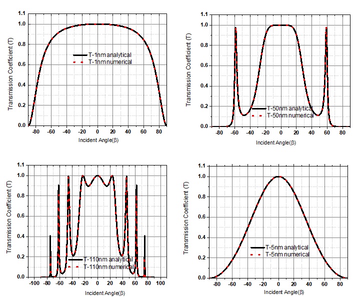
In the previous subsections II.1 and II.2, we have established a finite-difference numerical scheme and applied it to study tunneling transport of carriers through a biased potential barrier in graphene. As a validation, we first compare our finite-difference results with those from an analytical solution Neto et al. (2009) for a square potential barrier . Figure 1 displays a comparison for calculated transmission coefficients as a function of incident angle using either an analytical solution Neto et al. (2009) (black solid curves) or our finite-difference method presented in subsection II.2 (red dashed curves). The results in this figure clearly indicate that our finite-difference method in subsection II.2 is valid and can be applied to arbitrary potential profiles including a biased potential barrier.
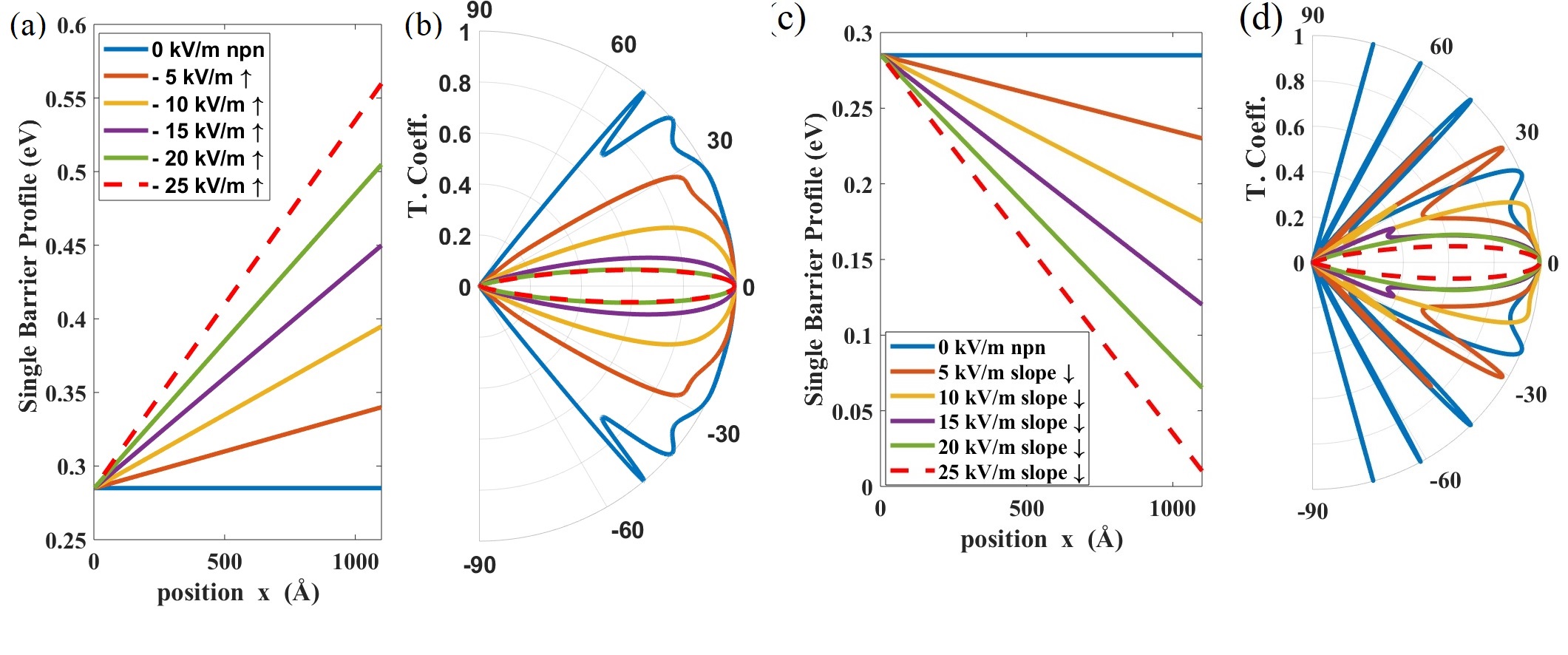
The numerical results of based on finite-difference method are presented in Fig. 2 as a function of incident angle for various values of bias field . Our results indicate that the Klein paradox, i.e., at , persists for all considered bias field values, either positive or negative. When is very small, large-angle resonant tunneling only occurs for or a reduced potential barrier but not for or an enhanced potential barrier. As becomes large, however, resonant tunneling are squeezed into a narrow angle region around (see Fig. 1 for a comparison). Such variations observed in can be attributed to the modification of a barrier potential profile by a bias field compared with a square potential barrier .
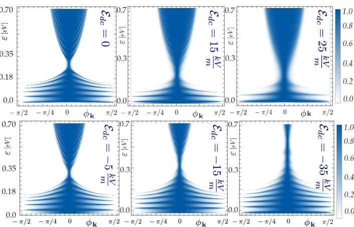
Figure 3 displays density plots of as functions of both incident energy and incident angle with six different values for bias field . We take the case with as a starting point, where the Klein paradox and collimation effect exist with many sharp resonances (branching and needling features) observed. As increases from zero to V/cm, these resonant branching and needling features are greatly obscured although the Klein paradox persists. On the other hand, as negative increases from zero to V/cm, both branching and needling regions expand significantly to higher incident energy range of electrons.
The calculated tunneling coefficient can be put into Eq. (15) to find tunneling conductivity or resistivity (its inverse) of ballistic electrons through a biased potential barrier in graphene. Here, the conductivity strongly depends on the bias field due to nonlinear nature of tunneling transport. For ballistic Dirac electrons in the absence of a potential barrier, their conductivity should be integer multiple of , as indicated by Eq. (15). In the presence of scattering by impurities or phonons, the occurring resistive force can give rise to a bias-dependent conductivity which is accompanied by a joule heating of electrons. Here, however, a bias-dependent conductivity is induced by a tunneling barrier which elastically and coherently reflects incoming electrons, leading to a destructive interference. Such a behavior can be attributed to a strong bias modulation ( dependence) of tunneling coefficient in Eq. (15).
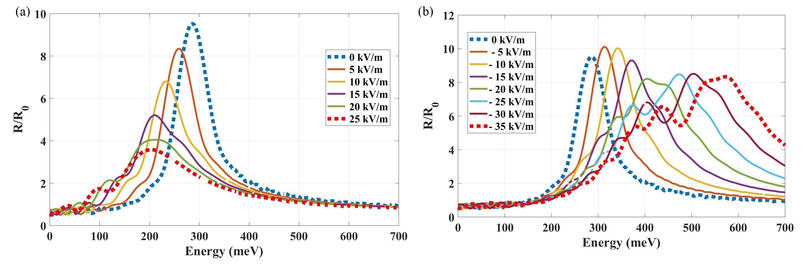
In Fig. 4, we present the calculated resistance ratios as functions of incident electron energy for different positive and negative biased potential barriers. We find from this figure that the resistance peak height decreases with increasing positive and the peak position shifts down to lower incident energy at the same time. For increasing negative , on the other hand, the peak position shifts upward with but the peak height remains nearly unchanged. Furthermore, the resistance peak is broadened with increasing , and the broadening effect becomes stronger for negative values.
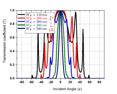
As shown in Fig. 5, the transmission coefficient at V/cm is suppressed only for large incident angles with increasing barrier width due to enlarged switching from a semi-classical regime to a quantum-tunneling regime inside barrier region, as well as due to interference effect in reflections from both barrier edges. Meanwhile, for around zero remains unchanged, leading to enhanced collimation of Dirac-electron tunneling.
III WKB Approximation for Wave Function and Transmission
In Section II, we have demonstrated a finite-difference approach for calculating Dirac-electron tunneling through an arbitrary potential barrier. In order to gain physics behind nonlinear transport of ballistic Dirac electrons tunneling, we introduce WKB approximation so as to analyze the dynamics of tunneling Dirac electrons in an explicit form beyond the numerical solution.
For this purpose, let us consider a tilted potential barrier, as shown in Fig. 7, with the potential , while outside of the barrier region. For this case, the effective dependent wave vector can be written as
| (20) |
where is the energy of an incoming particle, which is conserved for an elastic scattering with the barrier region, and . For a square potential barrier, as considered in Ref. [Neto et al., 2009], we simply set and will use it to build up our perturbation theory below.
We first introduce a unitary transformation for a gapless Dirac Hamiltonian, i.e., a -rotation around the axis, as employed in Ref. [Sonin, 2009], for simplification. This leads to the mixed eigen-function , where . If for a constant potential barrier, we find the eigen-function
| (21) |
where is the in-plane angle in the momentum space, , and the wave-function amplitude is independent of and .
In the most general case, the wave-function amplitudes satisfy the following equations Sonin (2009)
| (22) |
Throughout our derivation, the translational symmetry in the direction is always kept since our potential varies only along the axis. Therefore, we can simply write down . This simplify Eq. (22) into
| (23) |
where . As a special case, one can easily verify that the solution in Eq. (21) satisfies the above equation as or in Eq. (20) is taken for .
III.1 WKB Semi-Classical Approach
The general form of semi-classical WKB expansion for a tunneling-electron wave function can be expressed as Zalipaev et al. (2015)
| (24) |
where represents an action. Here, we will only consider the leading term in Eq. (24) and obtain
| (25) |
where and is independent of . Furthermore, we have also introduced the following two dimensionless quantities in Eq. (25)
| (26) | |||
where . It is straightforward to verify that the above solution becomes equivalent to that of gapless graphene as , given by Sonin (2009)
| (27) |
where has already been given by Eq. (20).
As an electron moves uphill with increasing potential, the sum of its potential and kinetic energies remains as a constant. Therefore, the kinetic energy of the electron decreases on its way. For this case, we need define a turning point of a semi-classical trajectory, at which but the total kinetic energy is still positive due to . We first find the turning point from in Eq. (20), where a Dirac electron turns into a Dirac hole. Moreover, the range corresponding to becomes a classically forbidden region in which become imaginary, where for . If this forbidden region lies entirely within the biased potential barrier region, the transmission coefficient is found to be Zalipaev et al. (2015)
| (28) |
which is a clear manifestation of the conservation of the Klein paradox for a biased potential barrier layer.
For the case with , the result in Eq. (28) could be generalized to
III.2 Perturbative Solution at Low Bias
We would like to emphasize that all the results obtained in previous subsection suffer a limitation, i.e., they are valid only if the electron-to-hole switching occurs inside the barrier region. However, this becomes invalid if either the slope of a potential profile or the barrier width becomes very small.
To seek for a perturbative solution within a barrier layer, we first assume a very small slope to ensure . We further assume so that particle-hole switching will not occur. As a result, the wave function takes the form and Eq. (23) can be applied to find solution for . In this case, however, a -rotation for is not needed.
For , the electron momentum is , where and . From this, we find , which becomes a small parameter in expansion. Based on these assumptions, we acquire a second-order differential equation with respect to the first wave-function component , yielding
| (30) |
Considering the fact that , we approximate the above equation as
| (31) |
Now, we look for a perturbative solution of Eq. (31) in the form of , and include only the terms up to the first non-vanishing linear correction to . Therefore, we get the th and st order equations, respectively,
| (32) | |||
| (33) |
Moreover, making use of the relation in Eq. (23) for two components of the wave function, i.e.,
| (34) |
we find
| (35) | |||
| (36) |
For the th order solution, we are dealing with the bias-free case having or a square potential barrier . From Eq. (32) we easily find its solution
| (37) |
which is a superposition of the forward and backward plane waves. Neto et al. (2009) In this case, from Eq. (35) the corresponding solution for the second component of the wave function is given by
where is the electron-hole index within the barrier region and for Dirac electrons inside the barrier region. Assuming , we always have and no electron-hole switching will occur. Two constants and in Eq. (III.2) can be determined by boundary conditions at both sides of a barrier layer.
| (39) |
where , and is the incident angle of Dirac electrons. Here, the transversal electron wave vector remains to be a constant during the whole tunneling process.
We first notice that and in Eqs. (37) and (III.2) are not normalized, and they can be determined by the first boundary condition at , giving rise to
| (40) | |||||
Here, and in Eq. (37) play the role of transmission and reflection amplitudes within the barrier region. Using the result in Eq. (40) and the second boundary condition at as well, we can further calculate the transmission coefficient as
| (41) |
which is identical to the corresponding results for a square potential barrier in Ref. [Neto et al., 2009], as expected.
In a similar way, we can find the st order solution from Eq. (33) for , yielding
| (42) | |||||
Here, the two new undetermined constants and are completely different from the zero-order constants and in Eq. (40), and they represent the first-order corrections to transmission and reflection amplitudes inside the barrier region. By using these calculated first wave-function components and in Eqs. (37) and (42), it is straightforward to find the second wave-function component from Eq. (36) although its explicit expression becomes a bit tedious to write out.
Now, we are able to determine the coefficients and in Eq. (42) and the correction to the transmission coefficient in Eq. (41). For this, we would like to write the transmission and reflection coefficients as and , corresponding to the wave functions in Eqs. (36) and (42). Using the two boundary conditions at and , we arrive at two equations for and , given by
| (49) | |||||
| (56) |
Finally, the transmission amplitude can be simply found from , where and are given by Eqs. (41) and (56), respectively.
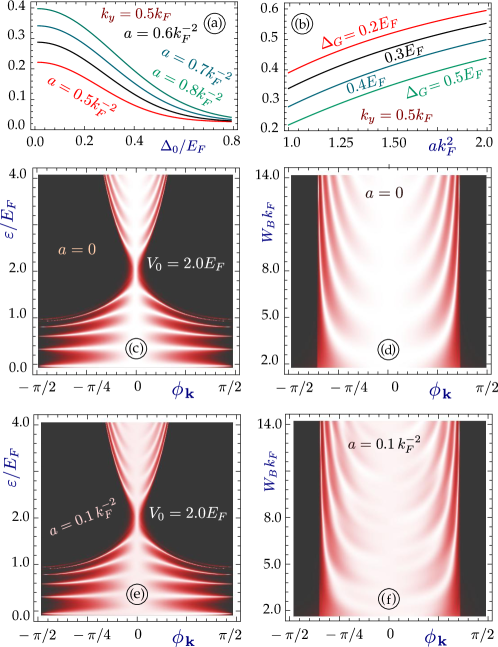
The numerical results from Eqs. (28) and (29) for a large electric bias are presented in panels and of Fig. 6. Here, a large graphene gap significantly suppresses for all values of , as shown in Fig. 6, while the increase of electric bias enhances for all values of , as seen in Fig. 6. From Figs. 6 and 6, we find that the full transmission for a head-on collision remains unchanged even under an electric bias . For small values, the electron-hole transition does not take place within the barrier region. Instead, a finite only slightly modifies the resonances of oblique tunneling but not the Klein paradox for the head-on collision.
IV Summary and remarks
In summary, we have developed a numerical approach for accurately calculating nonlinear tunneling transport of ballistic Dirac electrons through an arbitrary barrier potential in graphene. Here, our barrier-potential profile mimics a conventional MOSFET configuration where the square-barrier potential comes from the gate potential, and the barrier tilting connects to a source to drain applied bias. In addition, the barrier-potential profile can be tuned by applying a bias, and meanwhile the barrier height can be independently controlled by a gate voltage. Our research results can be applied to both sharp and smooth in-plane - junctions of either bipolar or unipolar devices. In the ballistic limit, we propose a mechanism by using barrier profile modulation for Dirac-electron tunneling, allowing an -- junction to be smoothly converted into a - junction with a proper choose of an applied bias.
In order to gain insight about the tunneling mechanism of Dirac electrons, we have introduced a perturbation theory for electron transmission through a slanted potential barrier with a small tilting compared to the inverse barrier width and characteristic electron momenta. In addition, we have derived a set of equations, corresponding to different orders of expansion parameter, and obtained analytical solutions of these equations. Furthermore, we have demonstrated how the tunneling resonances of a square potential barrier are affected under a finite bias voltage. Physically, we have extended a previously developed WKB theory for electron transmission in the opposite limit of a large bias, in which electron-to-hole switching occurs within the barrier region. Finally, a finite energy gap in graphene is included and we have shown that both head-on and skew transmissions will be suppressed exponentially due to existence of an energy gap and a large transverse momentum.
Another interesting implication is tunable filtering of Dirac electrons for nearly normal incidence, which might be utilized to design electronic lenses. The uniqueness of our mechanism is that we can specify a range for incident electron energies for focusing. Moreover, the electron resistance could be reduced and conductance minima can be shifted in energy just by controlling bias polarity, barrier height and the strength of bias field. Therefore, our model system can be employed to tune the refractive index of such a potential barrier in ballistic-electron optics. All these revealed properties are expected extremely valuable for the development of novel electronic and optical graphene-based devices.
Appendix A Exact Wave Function
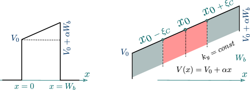
In this Appendix, we seek for an exact solution for the electron/hole wave function in the finite-slope region of a barrier, as seen in Fig. 7, with potential . If two boundaries of the barrier region stay far away from the electron-to-hole crossing point, i.e., , the wave function could be written as Sonin (2009)
| (57) |
where , , the symbol ⋆ means taking complex conjugation, and the two arbitrary constants and will be fixed by the boundary conditions on each side of the barrier region. Moreover, two functions and in Eq. (57) can be expressed by a Kummer confluent hypergeometric function as Sonin (2009)
| (58) | |||
The wave functions outside of the barrier region are easily obtained for the incoming and reflected waves, yielding
| (59) |
where . Similarly, for the transmitted wave we have
| (60) |
where . The transmission coefficient and the reflection coefficient can be obtained by matching the wave functions at two boundaries at and , i.e., and . Therefore, we acquire four equations for these two-components wave functions, which can be used to determine four unknowns , , , and , and the calculated will be further applied for evaluating the transmission .
Here, we would like to emphasize that although the obtained solution in Eq. (57) is exact, it holds true only for a very thick potential barrier with . Additionally, using this approach we can not address the limiting case with a small slope .
For the boundaries of a very thick potential barrier with a substantial slope , we find vary large absolute value of , and the wave function is calculated as
| (63) | |||
| (68) |
which gives rise to the transmission . This result is the same as that obtained from the a semi-classical theory.
References
- Katsnelson and Novoselov (2007) M. Katsnelson and K. Novoselov, Solid State Communications 143, 3 (2007).
- Neto et al. (2009) A. C. Neto, F. Guinea, N. M. Peres, K. S. Novoselov, and A. K. Geim, Reviews of modern physics 81, 109 (2009).
- Sarma et al. (2011) S. D. Sarma, S. Adam, E. Hwang, and E. Rossi, Reviews of modern physics 83, 407 (2011).
- Novoselov et al. (2005) K. S. Novoselov, A. K. Geim, S. Morozov, D. Jiang, M. I. Katsnelson, I. Grigorieva, S. Dubonos, Firsov, and AA, nature 438, 197 (2005).
- Wang et al. (2019) K. Wang, M. M. Elahi, L. Wang, K. M. Habib, T. Taniguchi, K. Watanabe, J. Hone, A. W. Ghosh, G.-H. Lee, and P. Kim, Proceedings of the National Academy of Sciences 116, 6575 (2019).
- Low and Appenzeller (2009) T. Low and J. Appenzeller, Physical Review B 80, 155406 (2009).
- Jang et al. (2013) M. S. Jang, H. Kim, Y.-W. Son, H. A. Atwater, and W. A. Goddard, Proceedings of the National Academy of Sciences 110, 8786 (2013).
- Wilmart et al. (2014) Q. Wilmart, S. Berrada, D. Torrin, V. H. Nguyen, G. Fève, J.-M. Berroir, P. Dollfus, and B. Plaçais, 2D Materials 1, 011006 (2014).
- Novoselov et al. (2006) K. S. Novoselov, E. McCann, S. Morozov, V. I. Fal’ko, M. Katsnelson, U. Zeitler, D. Jiang, F. Schedin, and A. Geim, Nature physics 2, 177 (2006).
- Zhang et al. (2005) Y. Zhang, Y.-W. Tan, H. L. Stormer, and P. Kim, nature 438, 201 (2005).
- Ohta et al. (2006) T. Ohta, A. Bostwick, T. Seyller, K. Horn, and E. Rotenberg, Science 313, 951 (2006).
- Cheianov and Fal’ko (2006) V. V. Cheianov and V. I. Fal’ko, Physical review b 74, 041403 (2006).
- Shytov et al. (2008) A. V. Shytov, M. S. Rudner, and L. S. Levitov, Physical review letters 101, 156804 (2008).
- Sonin (2009) E. Sonin, Physical Review B 79, 195438 (2009).
- Chen et al. (2016) S. Chen, Z. Han, M. M. Elahi, K. M. Habib, L. Wang, B. Wen, Y. Gao, T. Taniguchi, K. Watanabe, J. Hone, et al., Science 353, 1522 (2016).
- Cayssol et al. (2009) J. Cayssol, B. Huard, and D. Goldhaber-Gordon, Physical Review B 79, 075428 (2009).
- Allain and Fuchs (2011) P. E. Allain and J.-N. Fuchs, The European Physical Journal B 83, 301 (2011).
- Phong and Kong (2016) V. T. Phong and J. F. Kong, arXiv preprint arXiv:1610.00201 (2016).
- Cheianov et al. (2007) V. V. Cheianov, V. Fal’ko, and B. Altshuler, Science 315, 1252 (2007).
- Dahal and Gumbs (2017) D. Dahal and G. Gumbs, Journal of Physics and Chemistry of Solids 100, 83 (2017).
- Beenakker (2006) C. Beenakker, Physical review letters 97, 067007 (2006).
- Sajjad and Ghosh (2011) R. N. Sajjad and A. W. Ghosh, Applied Physics Letters 99, 123101 (2011).
- Elahi et al. (2019) M. M. Elahi, K. Masum Habib, K. Wang, G.-H. Lee, P. Kim, and A. W. Ghosh, Applied Physics Letters 114, 013507 (2019).
- Tworzydło et al. (2008) J. Tworzydło, C. Groth, and C. Beenakker, Physical Review B 78, 235438 (2008).
- Hernández and Lewenkopf (2012) A. R. Hernández and C. H. Lewenkopf, Physical Review B 86, 155439 (2012).
- Xu et al. (2010) G. Xu, X. Xu, B. Wu, J. Cao, and C. Zhang, Journal of Applied Physics 107, 123718 (2010).
- Low et al. (2009) T. Low, S. Hong, J. Appenzeller, S. Datta, and M. S. Lundstrom, IEEE Transactions on Electron Devices 56, 1292 (2009).
- Logemann et al. (2015) R. Logemann, K. Reijnders, T. Tudorovskiy, M. Katsnelson, and S. Yuan, Physical Review B 91, 045420 (2015).
- Ghobadi and Abdi (2013) N. Ghobadi and Y. Abdi, Current Applied Physics 13, 1082 (2013).
- Huang et al. (1999) D. Huang, A. Singh, and D. Cardimona, Physics Letters A 259, 488 (1999).
- Iurov et al. (2011) A. Iurov, G. Gumbs, O. Roslyak, and D. Huang, Journal of Physics: Condensed Matter 24, 015303 (2011).
- Iurov et al. (2013) A. Iurov, G. Gumbs, O. Roslyak, and D. Huang, Journal of Physics: Condensed Matter 25, 135502 (2013).
- Zhou et al. (2007) S. Y. Zhou, G.-H. Gweon, A. Fedorov, d. First, PN, W. De Heer, D.-H. Lee, F. Guinea, A. C. Neto, and A. Lanzara, Nature materials 6, 770 (2007).
- Giovannetti et al. (2007) G. Giovannetti, P. A. Khomyakov, G. Brocks, P. J. Kelly, and J. Van Den Brink, Physical Review B 76, 073103 (2007).
- Balog et al. (2010) R. Balog, B. Jørgensen, L. Nilsson, M. Andersen, E. Rienks, M. Bianchi, M. Fanetti, E. Lægsgaard, A. Baraldi, S. Lizzit, et al., Nature materials 9, 315 (2010).
- Kibis (2010) O. Kibis, Physical Review B 81, 165433 (2010).
- Kristinsson et al. (2016) K. Kristinsson, O. V. Kibis, S. Morina, and I. A. Shelykh, Scientific reports 6, 20082 (2016).
- Horing et al. (2016) N. Horing, A. Iurov, G. Gumbs, A. Politano, and G. Chiarello, Low-dimensional and nanostructured materials and devices (2016).
- Iurov et al. (2016) A. Iurov, G. Gumbs, D. Huang, and V. Silkin, Physical Review B 93, 035404 (2016).
- Pyatkovskiy (2008) P. Pyatkovskiy, Journal of Physics: Condensed Matter 21, 025506 (2008).
- Iurov et al. (2017) A. Iurov, G. Gumbs, D. Huang, and L. Zhemchuzhna, Journal of Applied Physics 121, 084306 (2017).
- Vargiamidis and Vasilopoulos (2014) V. Vargiamidis and P. Vasilopoulos, Applied Physics Letters 105, 223105 (2014).
- Zalipaev et al. (2015) V. Zalipaev, C. Linton, M. Croitoru, and A. Vagov, Physical Review B 91, 085405 (2015).