Efficient charge modulation in ultrathin LaAlO3-SrTiO3 field-effect transistors
Abstract
At the LaAlO3-SrTiO3 interface, electronic phase transitions can be triggered by modulation of the charge carrier density, making this system an excellent prospect for the realization of versatile electronic devices. Here, we report repeatable transistor operation in locally gated LaAlO3-SrTiO3 field-effect devices of which the LaAlO3 dielectric is only four unit cells thin, the critical thickness for conduction at this interface. This extremely thin dielectric allows a very efficient charge modulation of cm-2 within a gate-voltage window of V, as extracted from capacitance-voltage measurements. These also reveal a large stray capacitance between gate and source, presenting a complication for nanoscale device operation. Despite the small LaAlO3 thickness, we observe a negligible gate leakage current, which we ascribe to the extension of the conducting states into the SrTiO3 substrate.
Charge modulation in field-effect transistors (FETs) is the core physical mechanism enabling modern-day electronics. In a standard semiconductor such as silicon, its main purpose is to change the electrical conductivity, defining the “0” and “1” states in digital electronics. In other classes of materials, e.g., transition metal dichalcogenides and complex oxides, tuning the charge carrier density can trigger quantum phase transitions, offering possibilities for fundamental studies and for using such transitions in electronic devices Mannhart (1996); Ahn, Triscone, and Mannhart (2003); Mannhart and Schlom (2010). However, these transitions mostly take place at very high charge carrier densities, exceeding cm-2. Significant tuning of such a high charge carrier densities can only be achieved by means of chemical doping techniques and electrolyte gating, which are both impractical for functional devices.
In doped strontium titanate (SrTiO3) and at the conducting interface between SrTiO3 and selected other insulators such as LaAlO3, (super)conducting and insulating phases are near each other in terms of charge carrier density Schooley et al. (1965); Caviglia et al. (2008); Schneider et al. (2009); Liao et al. (2011), typically in the range of a few times cm-2. In the interface case, the geometry is intrinsically the same as the semiconductor-oxide stack of a metal-oxide-semiconductor FET (MOSFET), making such interfaces appealing for use in field-effect devices. Moreover, at low temperatures the SrTiO3 substrate can also be used as a gate dielectric (backgating), owing to its huge permittivity Weaver (1959). For the archetypical LaAlO3-SrTiO3 interface, reports on the significant field-effect tuning of the critical temperature for superconductivity Caviglia et al. (2008), the considerable low-temperature mobility Bell et al. (2009), and of spin-orbit coupling strength Caviglia et al. (2010); Ben Shalom et al. (2010) showed the versatility of this system both for fundamental studies and for its possible use in future electronics.
However, backgating takes place over large areas and requires the application of voltages in the order of 100 V across the typically 0.5-mm-thick SrTiO3 substrate to achieve a carrier density modulation of up to cm-2 electrostatically Caviglia et al. (2008). Hence, the backgating geometry is unsuitable for integration into circuits, which requires local operation by voltages of V. Achieving a MOSFET-like (topgate) geometry with the LaAlO3-SrTiO3 interface, where the voltage is applied across the LaAlO3 layer, is challenging because structuring these materials into (small) channels is not a trivial process Schneider et al. (2006). Low-voltage, topgate FETs were first realized by Förg and coworkers Förg, Richter, and Mannhart (2012), after which the functionality of such devices was extended greatly Hosoda et al. (2013); Eerkes, van der Wiel, and Hilgenkamp (2013); Jany et al. (2014). Unfortunately, the emergence of gate leakage currents across the thin LaAlO3 layer – typically 8 to 20 unit cells (uc) thick – limited the charge modulation to about cm-2. In parallel, the capability of achieving extreme charge modulations in SrTiO3-based FETs, up to a record value of cm-2, was demonstrated in inverted structures with a thick SrTiO3 layer as the dielectric Boucherit et al. (2013, 2014); Verma et al. (2014, 2016). Still, these devices have thick dielectrics and a high intrinsic carrier density, compromising low-voltage and local operation. The ultimate oxide-based FET, in which a small gate voltage achieves a charge modulation of several times cm-2, possibly enabling local switching of quantum phase transitions, therefore has remained elusive.
In this Letter, we demonstrate such efficient charge modulation in Au-LaAlO3-SrTiO3 FETs in which the LaAlO3 dielectric has a nominal thickness of only four unit cells (uc), the critical thickness for interface conduction Thiel et al. (2006). The devices display repeatable transistor behavior with low leakage currents and high ON/OFF ratios. Capacitance-voltage measurements reveal a large voltage-independent contribution to the capacitance, and a low effective permittivity for the LaAlO3 layer. The latter can be ascribed to a dielectric ‘dead layer’ forming on the Au-LaAlO3 interface, as indicated by scanning transmission electron microscopy. Despite this layer, the charge modulation is very efficient with a high capacitance per unit area, proving the principle of low voltage modulation of high charge densities in complex-oxide based FETs.
The fabrication of our devices started with a standard procedure to terminate the SrTiO3 substrate on the TiO2 sites of the (001) surface plane Koster et al. (1998). To enable structuring of the LaAlO3 film into channels, we deposited an AlOx layer at room temperature, which was etched in OPD4262 developer used for UV lithography Banerjee et al. (2012). The subsequent growth of LaAlO3 and Au by pulsed laser deposition (PLD) was done in situ, ensuring the interface between these layers to be as clean as possible. The LaAlO3 was deposited in an O2 process pressure of mbar at ∘C, with a laser fluence of 1.3 J cm-2, spot size of 2 mm2 and a frequency of 1 Hz, resulting in a growth rate of one uc per pulses, monitored by reflective high-energy electron diffraction (RHEED). The distance between the substrate and the single-crystalline target was 45 mm. After the LaAlO3 deposition, the sample was annealed for 1 h in an O2 pressure of 400 mbar at a temperature of 600 ∘C. Then, the Au was deposited in an Ar process pressure of 0.22 mbar, at ∘C with a laser fluence of 3.6 J cm-2 and a spot size of 1 mm2. To reduce the energy of the particles arriving at the substrate, the target-substrate distance was increased to 60 mm. This way, a layer of nm was grown after 9000 pulses at Hz. Then, electrical contacts to the interface were patterned using UV lithography, followed by a standard technique using Ar ion etching and subsequent sputtering of Ti/Au contacts Eerkes, van der Wiel, and Hilgenkamp (2013); Richter et al. (2013), which were structured by lift-off. Finally, the gate electrode was patterned using UV lithography and structured using a buffered KI solution Richter et al. (2013).
In the dc current-voltage measurements, the drain current, , was measured by a Keithley 2401 source-measure unit that also provided the drain-source voltage, . The gate current, , was determined by measuring the voltage over a k resistor using a Keithley 2000 multimeter. The capacitance-voltage characteristics were measured with a Keithley 4200-SCS parameter analyzer with a 4210 capacitance-voltage unit, using an ac voltage of mV and a frequency of kHz: close to the optimal frequency of kHz for these devices Schmitz et al. (2003). All measurements were performed at room temperature with the source terminal connected to ground.
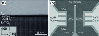
Figure 1 presents electron microscopy images of two of our devices. In the cross-sectional image (Fig. 1(a)), four unit cells of LaAlO3 are clearly visible. Like previously reported by another groupRichter et al. (2013), we also observe a thin disordered layer between the LaAlO3 and Au layer with a thickness of nm. The dark color indicates the absence of heavy elements such as Au, which appears light in this image; we therefore assume that this layer is not conducting and adds to the effective thickness of the dielectric. Further analysis of this layer is to be published elsewhere; we discuss the consequences of this layer for the transistor properties below. Figure 1(b) shows the top view of a FET.
Figure 2 summarizes the transistor operation of device A, a Au-LaAlO3-SrTiO3 FET like the one shown in Fig. 1(b), with a 4-uc-thin dielectric and channel length, , and width, , both equal to 10 m. We measured over ten devices on two different samples, with varying channel dimensions. All of these devices displayed transistor behavior, with ON/OFF ratios between and . In Fig. 2(a), we observe clear ohmic (triode/linear) and saturation (active) regimes. The circles separating these regimes represent the saturation voltage and current, which both increase monotonously with . For higher gate voltages, the saturation current does not follow the expected quadratic trend anymore Arora (2007), which we ascribe to a suppression of carrier mobility with increasing topgate voltage as previously observed Hosoda et al. (2013).
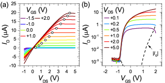
In Figure 2(b), switching of the channel conductivity is clearly demonstrated for all , from which we extract the transfer characteristics of this device. From a linear fit to versus , we determine the threshold voltage, , at V. The subthreshold swing of mV per decade – of which the minimum lies at , thus is not strictly threshold – and the maximum ON/OFF ratio of for V are quite comparable to the first semiconductor MOSFETs with a similar dielectric thickness Sasaki et al. (1996). Note that the ON/OFF ratio is limited by a finite OFF current, caused by a (minute) gate current emerging below V.
To further characterize our devices and to determine the charge modulation in the channel, we carried out capacitance-voltage measurements between gate and source. Using a simple model with a shunt and a series resistor next to the capacitance (Fig. 3(a)), we extract the capacitance-voltage characteristics of device A. The result, representative for all measured devices, is presented in Figure 3(b). The most prominent difference of this characteristic to semiconductor-based devices is that below threshold, the capacitance remains constant, instead of increasing due to the formation of an accumulation region Arora (2007). This voltage-independent capacitance at negative gate voltage is observed commonly in metal-LaAlO3-SrTiO3 junctions Jany et al. (2010); Li et al. (2011); Singh-Bhalla et al. (2011); Keun Kim et al. (2013) and is generally ascribed to a voltage-driven metal-insulator transition (MIT) Jany et al. (2010). When comparing this curve to Fig. 2(c), we find that the voltage-independent and voltage-dependent regions are separated by the threshold voltage of V.
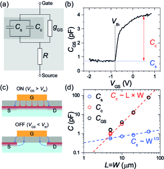
For a quantitative analysis, we assume that the voltage-independent, or ‘stray’, capacitance, , is a parallel element to the capacitance between the gate and the conducting channel, , yielding . To substantiate this assumption, we measured the capacitance-voltage characteristics of several devices with varying dimensions. This allows to extract the scaling of gate-source capacitance with device area, as depicted in Figure 3(d). Here, we consider devices with a square channel, i.e. , and extract the capacitances and at V, where the capacitance is fairly constant as function of gate voltage. We find that the total capacitance does not follow a power law dependence on , but that and do. The channel capacitance scales with device area (), in excellent agreement with a parallel-plate capacitor model. Hence, we can extract the effective relative permittivity, , using nm. The stray capacitance scales with the channel dimension to the power , thus depends on the geometry in a nontrivial way. To our knowledge, there is no theory yet that explains such a dependence on the device geometry. Extrapolation of our data suggests a crossover to occur at m, implying that the stray capacitance becomes dominant in small devices.
We postulate that this large stray capacitance is due to the very large permittivity of the channel material, SrTiO3, which is at room temperature Weaver (1959). As illustrated by the blue lines in Fig. 3(c), the gate terminal is capacitively coupled to the source and the drain through an electric field. The capacitance associated with this electric field depends on the permittivity of the insulator and of the channel material. In most materials, this would not be very significant; here, the very high permittivity of the channel material implies that the gate-source capacitance in absence of a conducting channel remains sizable.
To obtain the modulation of charge density in the channel, we omit the stray capacitance and integrate with respect to . Between threshold and V, this yields a carrier density modulation of cm-2. Above V, the measurement becomes inaccurate due to emerging gate leakage. If we assume that the capacitance remains constant above V, the projected charge modulation during the measurements presented in Fig. 2(b) is cm-2. The gate voltage required for this modulation does not exceed V; within this window, the gate leakage current remains more than an order of magnitude smaller than the current through the channel.
As a benchmark to compare these FETs to silicon-based devices, we calculate the equivalent oxide thickness (EOT) compared to SiO2, which has . Using and nm, we find an EOT of only nm. However, this value for is much lower than ones reported in literature for thick LaAlO3 films Edge et al. (2006); Robertson (2004), which range from to . This suppression of in metal-LaAlO3-SrTiO3 junctions is a widely observed phenomenon Jany et al. (2010); Li et al. (2011); Singh-Bhalla et al. (2011); Hosoda et al. (2013); Keun Kim et al. (2013); with increasing LaAlO3 layer thickness, was reported to approach the bulk value Hosoda et al. (2013). This was ascribed to a ‘dead layer’ forming inside the LaAlO3 film because of structural interface effects Stengel and Spaldin (2006). Because Fig. 1(a) shows a disordered layer forming on top of the fully intact, 4-uc-thin LaAlO3 layer, we propose an alternative scenario in which the ‘dead layer’ forms on top of the LaAlO3 rather than inside it. A series capacitor model in this scenario is mathematically equivalent to the one used by Hosoda et al. Hosoda et al. (2013):
| (1) |
By using , nm, and nm, we find , which we deem a reasonable value for a disordered layer. Therefore, this disordered layer at the LaAlO3-Au interface poses a viable alternative scenario to the dead layer within the LaAlO3 film; further investigations on devices with varying LaAlO3 layer thickness made using different fabrication procedures may distinguish between these two possibilities.
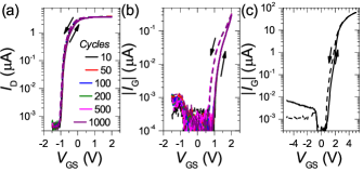
Despite the suppression of , the charge modulation in our devices is efficient and not compromised by gate leakage currents. Moreover, in comparison to previous reports on Au-LaAlO3-SrTiO3 stacks with 4-uc-thin barriers, where the gate current was used to perform tunneling spectroscopy of the interface Richter et al. (2013); Boschker et al. (2015); Kürten et al. (2017), the gate current density is about four orders of magnitude smaller. To investigate the factors determining the gate leakage current, we carried out temperature-dependent measurements as described in the Supplementary Information. The results show that ohmic and hopping-based conduction are negligible, and that the gate current is dominated by direct tunneling and Schottky emission. Accordingly, the density of defects inside the LaAlO3 layer must be very low and memristive effects based on the movement of defects should be absent. To confirm this, we measured the device response against repeated gate voltage cycling and up to high gate voltages of V. The results presented in Fig. 4 confirm the absence of resistive switching in our devices. Moreover, the behavior at high voltage in Fig. 4(c) fits the description of a Schottky diode with a forward-reverse bias ratio of , in good agreement with previous results Jany et al. (2010).
To explain the surprisingly large difference in gate current between the tunneling spectroscopy devices of Refs. (24; 35; 36) and our FETs, we consider the factors determining direct tunneling currents. Since both types of devices have the same material stack with the same thicknesses and the ‘dead layer’ is present in the tunneling spectroscopy studies Richter et al. (2013) as well, the energy landscape in terms of barriers and thickness should be the same. Therefore, we argue that the out-of-plane distribution of mobile charges in the SrTiO3 differs greatly between the two types of devices, increasing or decreasing the effective barrier thickness. In SrTiO3, the mobile charges do not reside exactly at the surface, but are distributed within a quantum well Biscaras et al. (2012); Gariglio, Fête, and Triscone (2015); Smink et al. (2017). This charge distribution depends crucially on the electrostatic boundary conditions for the well, which are highly susceptible to the environment in which the LaAlO3 film is grown Gunkel et al. (2016). In consequence, samples grown in different conditions have varying charge distributions in the quantum well. Especially for samples with thin LaAlO3 layers, the effective depth at which the mobile charges reside can thus vary greatly among samples grown under different conditions. We note that this effect may be enhanced greatly by a recently proposed region of negative polarization directly on the SrTiO3 side of the interface Raslan and Atkinson (2018). Of great importance for device operation is that this effective thickness increase should not suppress the capacitance by much, for the permittivity of SrTiO3 exceeds 300 even at room temperature Weaver (1959). Hence, we propose that this increase of the effective tunnel barrier thickness, without lowering the capacitance, is the key enabler of the efficient charge modulation observed in our devices.
In summary, we characterized the operation of Au-LaAlO3-SrTiO3 field-effect transistors with a LaAlO3 layer thickness of only four unit cells, or 1.5 nm. Our devices exhibit highly repeatable transistor behavior with very low gate leakage currents. In capacitance-voltage measurements, the gate-source capacitance becomes voltage-independent below threshold, which we attribute to stray fields coupling the gate to the source and drain terminals in absence of a conducting channel. Integration of the voltage-dependent part of the capacitance yields a charge modulation of about cm-2, within a gate voltage range of V.
This highly efficient charge modulation is limited by a commonly observed suppression of the permittivity in very thin LaAlO3 layers grown on SrTiO3. Scanning transmission electron microscopy imaging suggests that this suppression is due to a dielectric ‘dead layer’ forming at the Au-LaAlO3 interface, with a thickness of nm. The surprisingly low leakage current cannot be due to this layer, but is likely due to the out-of-plane distribution of charges in the SrTiO3 channel. Because of the high dielectric permittivity of SrTiO3, this does not significantly affect the gate-source capacitance, enabling efficient modulation of high charge densities by low gate voltages without excessive gate leakage currents. We foresee that making use of this delocalization in quantum wells opens new venues to engineer high-charge-density field-effect transistors based on advanced materials.
Acknowledgements.
We thank Maurits de Jong for his help with the capacitance-voltage measurements, Jochen Mannhart and Hans Boschker for stimulating discussions, and Frank Roesthuis, Dick Veldhuis, and Thijs Bolhuis for technical assistance. We acknowledge financial support through the DESCO program of the Foundation for Fundamental Research on Matter (FOM), associated with the Netherlands Organization for Scientific Research (NWO).References
- Mannhart (1996) J. Mannhart, “High- transistors,” Superconductor Science and Technology 9, 49–67 (1996).
- Ahn, Triscone, and Mannhart (2003) C. H. Ahn, J.-M. Triscone, and J. Mannhart, “Electric field effect in correlated oxide systems,” Nature 424, 1015–1018 (2003).
- Mannhart and Schlom (2010) J. Mannhart and D. G. Schlom, “Oxide Interfaces–An Opportunity for Electronics,” Science 327, 1607–1611 (2010).
- Schooley et al. (1965) J. F. Schooley, W. R. Hosler, E. Ambler, J. H. Becker, M. L. Cohen, and C. S. Koonce, “Dependence of the Superconducting Transition Temperature on Carrier Concentration in Semiconducting SrTiO3,” Physical Review Letters 14, 305 (1965).
- Caviglia et al. (2008) A. D. Caviglia, S. Gariglio, N. Reyren, D. Jaccard, T. Schneider, M. Gabay, S. Thiel, G. Hammerl, J. Mannhart, and J.-M. Triscone, “Electric field control of the LaAlO3/SrTiO3 interface ground state,” Nature 456, 624–627 (2008).
- Schneider et al. (2009) T. Schneider, A. D. Caviglia, S. Gariglio, N. Reyren, and J.-M. Triscone, “Electrostatically-tuned superconductor-metal-insulator quantum transition at the LaAlO3 / SrTiO3 interface,” Physical Review B 79 (2009), 10.1103/PhysRevB.79.184502.
- Liao et al. (2011) Y. C. Liao, T. Kopp, C. Richter, A. Rosch, and J. Mannhart, “Metal-insulator transition of the LaAlO3 -SrTiO3 interface electron system,” Physical Review B 83, 075402 (2011).
- Weaver (1959) H. Weaver, “Dielectric properties of single crystals of SrTiO3 at low temperatures,” Journal of Physics and Chemistry of Solids 11, 274–277 (1959).
- Bell et al. (2009) C. Bell, S. Harashima, Y. Kozuka, M. Kim, B. G. Kim, Y. Hikita, and H. Y. Hwang, “Dominant Mobility Modulation by the Electric Field Effect at the LaAlO3/SrTiO3 Interface,” Physical Review Letters 103, 226802 (2009).
- Caviglia et al. (2010) A. D. Caviglia, M. Gabay, S. Gariglio, N. Reyren, C. Cancellieri, and J.-M. Triscone, “Tunable Rashba Spin-Orbit Interaction at Oxide Interfaces,” Physical Review Letters 104, 126803 (2010).
- Ben Shalom et al. (2010) M. Ben Shalom, M. Sachs, D. Rakhmilevitch, A. Palevski, and Y. Dagan, “Tuning Spin-Orbit Coupling and Superconductivity at the SrTiO3/LaAlO3 Interface: A Magnetotransport Study,” Physical Review Letters 104, 126802 (2010).
- Schneider et al. (2006) C. W. Schneider, S. Thiel, G. Hammerl, C. Richter, and J. Mannhart, “Microlithography of electron gases formed at interfaces in oxide heterostructures,” Applied Physics Letters 89, 122101 (2006).
- Förg, Richter, and Mannhart (2012) B. Förg, C. Richter, and J. Mannhart, “Field-effect devices utilizing LaAlO3-SrTiO3 interfaces,” Applied Physics Letters 100, 053506 (2012).
- Hosoda et al. (2013) M. Hosoda, Y. Hikita, H. Y. Hwang, and C. Bell, “Transistor operation and mobility enhancement in top-gated LaAlO3/SrTiO3 heterostructures,” Applied Physics Letters 103, 103507 (2013).
- Eerkes, van der Wiel, and Hilgenkamp (2013) P. D. Eerkes, W. G. van der Wiel, and H. Hilgenkamp, “Modulation of conductance and superconductivity by top-gating in LaAlO3/SrTiO3 2-dimensional electron systems,” Applied Physics Letters 103, 201603 (2013).
- Jany et al. (2014) R. Jany, C. Richter, C. Woltmann, G. Pfanzelt, B. Förg, M. Rommel, T. Reindl, U. Waizmann, J. Weis, J. A. Mundy, D. A. Muller, H. Boschker, and J. Mannhart, “Monolithically Integrated Circuits from Functional Oxides,” Advanced Materials Interfaces 1, 1300031 (2014).
- Boucherit et al. (2013) M. Boucherit, O. F. Shoron, T. A. Cain, C. A. Jackson, S. Stemmer, and S. Rajan, “Extreme charge density SrTiO/GdTiO heterostructure field effect transistors,” Applied Physics Letters 102, 242909 (2013).
- Boucherit et al. (2014) M. Boucherit, O. Shoron, C. A. Jackson, T. A. Cain, M. L. C. Buffon, C. Polchinski, S. Stemmer, and S. Rajan, “Modulation of over 10 cm electrons in SrTiO/GdTiO heterostructures,” Applied Physics Letters 104, 182904 (2014).
- Verma et al. (2014) A. Verma, S. Raghavan, S. Stemmer, and D. Jena, “Au-gated SrTiO3 field-effect transistors with large electron concentration and current modulation,” Applied Physics Letters 105, 113512 (2014).
- Verma et al. (2016) A. Verma, K. Nomoto, W. S. Hwang, S. Raghavan, S. Stemmer, and D. Jena, “Large electron concentration modulation using capacitance enhancement in SrTiO/SmTiO Fin-field effect transistors,” Applied Physics Letters 108, 183509 (2016).
- Thiel et al. (2006) S. Thiel, G. Hammerl, A. Schmehl, C. W. Schneider, and J. Mannhart, “Tunable Quasi-Two-Dimensional Electron Gases in Oxide Heterostructures,” Science 313, 1942–1945 (2006).
- Koster et al. (1998) G. Koster, B. L. Kropman, G. Rijnders, D. H. A. Blank, and H. Rogalla, “Quasi-ideal strontium titanate crystal surfaces through formation of strontium hydroxide,” Applied Physics Letters 73, 2920 (1998).
- Banerjee et al. (2012) N. Banerjee, M. Huijben, G. Koster, and G. Rijnders, “Direct patterning of functional interfaces in oxide heterostructures,” Applied Physics Letters 100, 041601 (2012).
- Richter et al. (2013) C. Richter, H. Boschker, W. Dietsche, E. Fillis-Tsirakis, R. Jany, F. Loder, L. F. Kourkoutis, D. A. Muller, J. R. Kirtley, C. W. Schneider, and J. Mannhart, “Interface superconductor with gap behaviour like a high-temperature superconductor,” Nature 502, 528–531 (2013).
- Schmitz et al. (2003) J. Schmitz, F. N. Cubaynes, R. J. Havens, R. d. Kort, A. J. Scholten, and L. F. Tiemeijer, “RF capacitance-voltage characterization of MOSFETs with high leakage dielectrics,” IEEE Electron Device Letters 24, 37–39 (2003).
- Arora (2007) N. Arora, Mosfet Modeling for VLSI Simulation: Theory and Practice, International series on advances in solid state electronics and technology (World Scientific, 2007).
- Sasaki et al. (1996) H. Sasaki, M. Ono, T. Yoshitomi, T. Ohguro, S. Nakamura, M. Saito, and H. Iwai, “1.5 nm direct-tunneling gate oxide Si MOSFET’s,” IEEE Transactions on Electron Devices 43, 1233–1242 (1996).
- Jany et al. (2010) R. Jany, M. Breitschaft, G. Hammerl, A. Horsche, C. Richter, S. Paetel, J. Mannhart, N. Stucki, N. Reyren, S. Gariglio, P. Zubko, A. D. Caviglia, and J.-M. Triscone, “Diodes with breakdown voltages enhanced by the metal-insulator transition of LaAlO3-SrTiO3 interfaces,” Applied Physics Letters 96, 183504 (2010).
- Li et al. (2011) L. Li, C. Richter, S. Paetel, T. Kopp, J. Mannhart, and R. C. Ashoori, “Very Large Capacitance Enhancement in a Two-Dimensional Electron System,” Science 332, 825–828 (2011).
- Singh-Bhalla et al. (2011) G. Singh-Bhalla, C. Bell, J. Ravichandran, W. Siemons, Y. Hikita, S. Salahuddin, A. F. Hebard, H. Y. Hwang, and R. Ramesh, “Built-in and induced polarization across LaAlO3/SrTiO3 heterojunctions,” Nature Physics 7, 80–86 (2011).
- Keun Kim et al. (2013) S. Keun Kim, S.-I. Kim, J.-H. Hwang, J.-S. Kim, and S.-H. Baek, “Capacitance-voltage analysis of LaAlO3/SrTiO3 heterostructures,” Applied Physics Letters 102, 112906 (2013).
- Edge et al. (2006) L. F. Edge, D. G. Schlom, P. Sivasubramani, R. M. Wallace, B. Holländer, and J. Schubert, “Electrical characterization of amorphous lanthanum aluminate thin films grown by molecular-beam deposition on silicon,” Applied Physics Letters 88, 112907 (2006).
- Robertson (2004) J. Robertson, “High dielectric constant oxides,” The European Physical Journal Applied Physics 28, 265–291 (2004).
- Stengel and Spaldin (2006) M. Stengel and N. A. Spaldin, “Origin of the dielectric dead layer in nanoscale capacitors,” Nature 443, 679–682 (2006).
- Boschker et al. (2015) H. Boschker, C. Richter, E. Fillis-Tsirakis, C. W. Schneider, and J. Mannhart, “Electron-phonon Coupling and the Superconducting Phase Diagram of the LaAlO3-SrTiO3 Interface,” Scientific Reports 5, 12309 (2015).
- Kürten et al. (2017) L. Kürten, C. Richter, N. Mohanta, T. Kopp, A. Kampf, J. Mannhart, and H. Boschker, “In-gap states in superconducting LaAlO3-SrTiO3 interfaces observed by tunneling spectroscopy,” Physical Review B 96, 014513 (2017).
- Biscaras et al. (2012) J. Biscaras, N. Bergeal, S. Hurand, C. Grossetête, A. Rastogi, R. C. Budhani, D. LeBoeuf, C. Proust, and J. Lesueur, “Two-Dimensional Superconducting Phase in LaTiO3/SrTiO3 Heterostructures Induced by High-Mobility Carrier Doping,” Physical Review Letters 108, 247004 (2012).
- Gariglio, Fête, and Triscone (2015) S. Gariglio, A. Fête, and J.-M. Triscone, “Electron confinement at the LaAlO3/SrTiO3 interface,” Journal of Physics: Condensed Matter 27, 283201 (2015).
- Smink et al. (2017) A. E. M. Smink, J. C. de Boer, M. P. Stehno, A. Brinkman, W. G. van der Wiel, and H. Hilgenkamp, “Gate-Tunable Band Structure of the LaAlO3-SrTiO3 Interface,” Physical Review Letters 118 (2017).
- Gunkel et al. (2016) F. Gunkel, R. Waser, A. H. H. Ramadan, R. A. De Souza, S. Hoffmann-Eifert, and R. Dittmann, “Space charges and defect concentration profiles at complex oxide interfaces,” Physical Review B 93, 245431 (2016).
- Raslan and Atkinson (2018) A. Raslan and W. A. Atkinson, “Possible flexoelectric origin of the Lifshitz transition in LaAlO3/SrTiO3 interfaces,” Physical Review B 98, 195447 (2018).