Gallium-Boron-Phosphide (GaBP2): A New III-V Semiconductor for Photovoltaics
Abstract
Using machine learning (ML) approach, we unearthed a new III-V semiconducting material having an optimal bandgap for high efficient photovoltaics with the chemical composition of Gallium-Boron-Phosphide (GaBP2, space group: Pna21). ML predictions are further validated by state of the art ab-initio density functional theory (DFT) simulations. The stoichiometric Heyd-Scuseria-Ernzerhof (HSE) bandgap of GaBP2 is noted to 1.65 eV, a close ideal value (1.4-1.5 eV) to reach the theoretical Queisser-Shockley limit. The calculated electron mobility is similar to that of silicon. Unlike perovskites, the newly discovered material is thermally, dynamically and mechanically stable. Above all the chemical composition of GaBP2 are non-toxic and relatively earth-abundant, making it a new generation of PV material. Using ML, we show that with a minimal set of features the bandgap of III-III-V and II-IV-V semiconductor can be predicted up to an RMSE of less than 0.4 eV. We presented a set of scaling laws, which can be used to estimate the bandgap of new III-III-V and II-IV-V semiconductor, with three different crystal phases, within an RMSE of 0.5 eV.
I Introduction
Photovoltaic (PV) conversion is the direct conversion of light into electricity and thus has a true potential to replace fossil fuel based energy resources which have harmful consequences on nature. One of the major components of the PV devices is the light-absorbing material that consists predominantly of semiconducting materials with an electronic bandgap (Eg) characteristic. The suitability of these PV materials is evaluated by two major properties: (i) its capability of absorption of incident light (absorption coefficient) and creation of electron-hole (e-h) pair and (ii) their ability to transport these e-h carriers from semiconducting material to electrical contacts. There are a few other criteria to follow while selecting PV material such as its toxicity, and its constituent’s earth abundant etc.
In their classic work, William Shockley and Hans J. Queisser Shockley and Queisser (1961); Miller et al. (2012) showed that for a single junction solar cell the maximum theoretical efficiency can be 33.5% given that the Eg of the semiconductor is 1.4-1.5 eV Shockley and Queisser (1961); Grätzel (2001). Most of the commercialized PV devices that are available to us now are made of classical semiconducting materials silicon (Si) Priolo et al. (2014) which has Eg of 1.1 eV. The recorded efficiency of Si based solar cell is 6% for amorphous and 25% in single crystalline and single junction configurations Green (2009). Such a lower value of efficiency is caused by its inherent material properties of its indirect Eg Priolo et al. (2014). Other than Si, only a limited number of semiconductor composed of III-V and II-VI elements possess the desired value and nature of Eg Curtarolo et al. (2013), many of which contain indium (In), which has a very low earth abundance. Gallium Arsenide (GaAs), which is a binary III-V semiconductor having a direct bandgap of 1.4 eV, also have been proposed to be another prominent candidate for PV application but the maximum recorded efficiency of GaAs based solar cell Greenu et al. (2015) is at 28.8% which is still 4.7% away from the theoretical limit. Further to achieve the maximum value of the theoretical limit of PV plenty of other different materials are explored in past including CdTe and perovskites. Nonetheless their efficiency is lower than the GaAs itself Singh and Ravindra (2012); Wesoff (2016); Peters and Buonassisi (2018) till date. In recent times organic-inorganic metal halide perovskite draws tremendous attention due to its high efficiency ( 23.7%) Wang et al. (2019); Meng et al. (2018). Yet their poor material stability has hindered their commercial applications.
Recent success in synthesis and stabilization of ternary and quaternary semiconductors through the cation mutation of III-V and II-IV-V semiconductors opens up a set of materials Lahourcade et al. (2013); Senabulya et al. (2016); Feldberg et al. (2013); Skachkov et al. (2016); Zakutayev et al. (2014). Predominantly they crystallize in three different structural phases, namely (i) Wurtzite-kesterite (KT) (space group: Pna21) (ii) Wurtzite-stannite (ST) (space group:Pc) and (iii) chalcopyrite (CP) (space group: I2d ). Recent studies show that semiconducting material composed of elements from group-II, group IV and V as well as group-III and V in ABX2 form can absorb visible light Wang et al. (2014); Fioretti et al. (2015). This further suggests that ABX2 [A={Al, Ga, Zn, Cd}, B={Ga, In, Ge, Sn, Si} and X = {N, P, As, Sb}] can be a new generation materials for PV application Fioretti et al. (2015); Feldberg et al. (2013); Martinez et al. (2016). One of the interesting and important properties of ABX2 is their higher degrees of tunability of Eg by foreign element substitution, alloying, and phase engineering Wang et al. (2014); Fioretti et al. (2015); Narang et al. (2014).
Pandey et al.’s Pandey et al. (2017) theoretical work suggests a few semiconducting materials with Eg of 1.4 eV namely, ZnSnP2, CdSiAs2, GaInN2, ZnSiP2, AlInAs2, CdGeP2, AlInAs2 etc. It is to note that toxicity is one of the biggest disadvantages for compound which contains element like arsenic and cadmium. Further, there are many reports in the literature which hinting that indium (In) has a tendency of forming metallic cluster (or segregation) inside the material. This has a detrimental effect to the device performance of In-based semiconductorsTang et al. (2015); Lee et al. (2018); Reyes et al. (2013); Martini et al. (2003); Barlow et al. (2018); Mannarino et al. (2015). Further ZnSnP2 which has a experimental Eg of 1.7 eV shows a order-disorder phase transition at high temperature which reduce the Eg to 0.75 eV Scanlon and Walsh (2012). The experimental Eg of ZnSiP2 in CP phase is 2.1 eV a bit higher for use in single junction solar cell but can be used for multijunction tandem devices Martinez et al. (2016). Theoretical work of Gautam et al. shows that the higher theoretical limit of efficiency of CdGeP2 based solar cell is 22.6% Gautam et al. (2015) which is less than the efficiency of Si based solar cell. Because of all the above issues, finding new materials in the ABX2 family is essential for designing efficient PV devices. In all of these studies mentioned earlier, the inclusion of boron in ABX2 materials were neglected completely. In this regard, the property of the boron based ABX2 semiconducting materials are fundamentally important too. In this work, we explore material properties such as Eg of boron based III-III-V2 materials and discussed its viability in PV and/or other optoelectronic applications. We substituted boron at both A and B sites of ABX2 independently along with other group-III elements such as (In,Ga,Al) which gives us 24 new sets of materials in one phase alone.
Most conventional ways to find the Eg of semiconducting materials are
-
1.
Optical Spectroscopy or electrical transport characterization of chemically synthesized samples
-
2.
Ab-initio Density Functional Theory (DFT) simulations (Using Heyd-Scuseria-Ernzerhof (HSE) and/or GW approximation)
Both these above mentioned techniques required a substantial amount of experimental and computational resources respectively and are time consuming process especially for large set of samples. Recent development of machine learning (ML) based approach has shown a great promise in predicting material properties Butler et al. (2018); Sparks et al. (2016); Xue et al. (2017) within a fraction of a second. Gamst et al. predicted the mechanical hardness of poly-crystalline inorganic compounds using neural network De Jong et al. (2016). Further Zheng et al. classify the stability of full-Heusler compounds using convolutional neural networks (CNN) Zheng et al. (2018). Ramprasad et al. predicted the various material properties such as atomization energy, crystal structure, electron affinity, dielectric constant, formation energy etc using multiple ML models Pilania et al. (2013). Motivated by the above works, we explore various supervised ML models to predict Eg of ABX2 compounds and used the trained model to predict bandgap of boron based compounds. We validate the ML-predicted Eg of newly predicted materials using ab-initio DFT calculations where mBJ and HSE06 functional are used. We find that our ML predicted and DFT-calculated Eg values are in good agreement. By imposing various criteria that is necessary for a good PV material we filtered new semiconductor for efficient PV applications.
To this end, we arrange the rest of the paper in the following order;
-
1.
Section II deals with the methods of ML models and ab-initio simulations
-
2.
In section III we discussed the predictability of our ML models and filter new materials for PV application with suitable Eg
-
3.
We validate the Eg of newly predicted material using ab-initio calculations in section IV. We further studied their structural, electronic, transport properties as well as stability and further filtered them for PV applications.
II Methods
II.1 Dataset selection
To train the ML models, we used the data-set generated by Pandey et al. Pandey et al. (2017) where Eg of ABX2 [A={Al, Ga, Zn, Cd}, B={Ga, In, Ge, Sn, Si} and X = {N, P, As, Sb}] type stoichiometric semiconductor are computed with first-principle DFT simulations. It is well known to the literature that local and semilocal approaches severely underestimate the Eg of materials. To overcome this issue, the authors included the meta-GGA GLLB-SC functional in their calculations and showed that the calculated Eg is in good agreement with the experiment Pandey et al. (2017). In their work the author chose three different crystal structure i,e. (i) KT, (ii) ST and (iii) CP phases Goodman (1957); Jaffe and Zunger (1984). Details of their computational technique and numerical parameters are discussed in Reference Pandey et al., 2017. The data-set contains relatively a small number of entry ( 100).
II.2 Features selection
In predictions of Eg of ABX2 type compounds semiconductor, we include various properties of the compositional elements of ABX2 as features. They are (1) atomic number (AN), (2) atomic mass (AM), (3) period (P) and (4) group in the periodic table (G), (5) first ionization energy (FIE), (6) second ionization energy (SIE), (7) electron affinity (EA), (8) Pauling electronegativity , (9) Allen electronegativity (AEN), (10) Van der Waals radius , (11) covalent radius , (12) atomic radius , (13) melting point (MP), (14) boiling point (BP), (15) density , (16) molar volume , (17) heat of fusion , (18) heat of vaporization , (19) thermal conductivity , and (20) specific heat etc. We considered volume of the unit cell (V) also to a component to feature vector. We classify the crystal phase of the materials using one-hot encoding technique in our work. The numerical values of features are given in section I of Supplementary Information (SI).
II.3 Machine learning methods
In constructing the ML models, we employed various linear [e.g. Ordinary Least Square (OLS), Partial Least Square (PLS), Ridge and least absolute shrinkage and selection operator (Lasso)] and non-linear regression [e.g. Gradient Boosting Regression (GBR), Kernel Ridge Regression (KRR), Random Forest Regression (RFR), Support Vector Machine (SVM), Artificial Neural Network (ANN)] methods via Scikit-Learn library F et al. (2011). We also checked the prediction power of recently developed XG-Boost regression (XGB) technique Chen and Guestrin (2016) in this study. Details of the hyperparameters used in these models are discussed in section II of SI. We chose 75% of the data to train models while remaining data to test them. The Monte Carlo cross-validation method is used to evaluates their predictability. Before the machine learning regression, the feature vectors were normalized. We assessed the prediction power of ML models with help of root mean square error (RMSE) and R2 value of test dataset.
II.4 Ab-initio computational details
Ab-initio Density Functional Theory (DFT) simulations were carried out using Vienna ab-initio simulation package (VASP) where projector augmented wave method (PAW) was used Kresse and Furthmüller (1996a, b); Kresse and Joubert (1999). A generalized gradient approximation proposed by Perdew-Burke- Ernzerhof Perdew et al. (1996) was used for calculation of the exchange and correlation energy. Brillouin zone is sampled on a -centred (867 for KT, ST and 888 for CP phase) uniform mesh of k-points in a unit cell of reciprocal space Monkhorst and Pack (1976). A plane wave cutoff energy of 520 eV was used in our simulations. Positions of all the atoms were allowed to relax to minimize energy until forces on each atom were less than 10-3 eV/. To correct the known underestimation of Eg by DFT-PBE, we included modified Becke-Johnson exchange (mBJ) potential and Becke and Johnson (2006) and Heyd-Scuseria-Ernzerhof (HSE) screened Coulomb hybrid functional Heyd et al. (2005) in our calculations. In calculation with HSE functional, we used 25% of the Hartree-Fock exchange potential. The screening parameter was fixed at 0.2. The dynamical stability of materials was studied using Density Functional Perturbation Theory (DFPT). The electronic transport properties were calculated by solving Boltzmann transport equation (BTE) as implemented in AMMCR code Mandia et al. (2019a).


III Machine Learning Formulation and Screening of Photo-Voltaic Materials
We begin our prediction of Eg using the features as discussed in section II. The predictability of different models are compared (see Fig.1) and we find that predictability of non-linear models are better comparison to linear models (i.e. low RMSE in predictions and better R2) in prediction of . The RMSEs (standard deviation (SD)) in training and testing cases in various linear models are essentially the same and are 0.45 (0.02) and 0.55 (0.08) eV respectively. Non-linear model like KRR, GBR, RFR, SVM, ANN and XGB predicts the Eg up to an RMSE(SD) of 0.31(0.07), 0.31(0.11), 0.43 (0.11), 0.33 (0.12), 0.42 (0.13) and 0.37 (0.12) eV respectively. We further compared our prediction accuracy with the recently published work in the literature. Recent work of Huang et al. predicts the Eg of binary nitrides material with SVR up to an RMSE of 0.298 eV Huang et al. (2019). By using a relatively larger dataset of MXenes materials Ranjan et al. showed a better prediction accuracy (test RMSE of 0.20 eV) Rajan et al. (2018). Olsthoorn et al. predicted the Eg of organic crystal up to an RMSE of 0.5 eV Olsthoorn et al. . The Eg predicted by ML for double perovskite materials are within the RMSEs of 0.8-1.0 eV Pilania et al. (2013). Similarly, the work of Sotskov et al. Sotskov et al. (2018) showed a relatively low accuracy in predictions of Eg of inorganic materials. Thus, in general our prediction accuracy of Eg in ABX2 materials are within the error broadly reported in the literature which further suggests, we have achieved to build a working ML model with the optimal set of hyperparameters.
Based on the important features in the prediction of the Eg we minimized the number of feature to 17, which includes one-hot encoding of the phase of materials. Feature weightage are listed in section III of SI. The relative weightage of all 17 features are shown in a pie-chart plot as Fig.2(b) when predictions are made with top 17 features only. We find very little change in the prediction error in comparison to the 64 features. We note that the volume of the unit cell (V) is the predominant factor that determines the Eg of ABX2 materials. (see Fig.2(b)). Fitting of the empirical relation between Eg and square of lattice parameter (or V2/3 in our model) Dalven (1973) to the data reveals two different classes and hence two sets of coefficient (see Eqn.1). We find that when the volume is less than 246 (i.e. for ABN2) the Eg increases quite rapidly with decrease in the V. Compound having anions as P, As, and Sb shows a rather slower changes in the Eg with changes in V. Statistically, it can be observed that a non-nitride ABX2 material with unit cell volume of 300-420 can have a band-gap of 1.4-1.5 eV which is ideal for PV applications.
| (1) |

It is quite clear by this point that prediction of Eg with ML, V is not only important but also necessary. As volume can only be calculated by only DFT or experimentally (X-ray diffraction method), without a further ML model for V, our previous model for Eg will be not effective. Thus, we designed a ML model to predict the V. Interestingly, with the LASSO regression, we predict V quite accurately (up to an RMSE of 5.3 ) (see Fig.3). Based on which we establish a relation between V and atomic features (see Eqn.2) of the constituent elements;
| (2) |
where s are in picometer(pm) unit.
| Compound | Scaling- | DFT-PBE | Eg | ML-Eg | ML-Eg | DFT-mBJ | DFT-HSE06 | DFT-PBE |
| Name | Volume () | Volume () | (Eqn.1) (eV) | (RFR) (eV) | (XGB) (eV) | Eg (eV) | Eg (eV) | (eV/atom) |
| AlBAs2 | 290.0 | 293.5 | 2.30 | 1.47 | 1.53 | 2.63 | - | - |
| AlBP2 | 240.8 | 253.7 | 3.41 | 2.09 | 1.61 | 1.65 | - | -0.35 |
| BAlP2 | 250.1 | 253.6 | 3.17 | 2.4 | 2.63 | 1.65 | 1.83 | -0.35 |
| BAlSb2 | 380.7 | 380.3 | 0.91 | 1.59 | 2.03 | 0.63 | - | - |
| BGaSb2 | 382.7 | 376.4 | 0.88 | 1.31 | 1.5 | - | 0.92 | - |
| GaBP2 | 242.4 | 253.5 | 3.37 | 1.51 | 1.56 | 1.50 | 1.65 | -0.27 |
| InBP2 | 277.8 | 286.6 | 2.54 | 1.47 | 1.51 | 1.20 | 1.55 | -0.09 |
Further, we extend our work to predict the Eg of ABX2 for boron at A and B sites independently by which we generate 24 new configurations. At first, we predict their volumes using Eqn.2. Based on our initial assessment, we find that inclusion of boron in ABN2 material predicts a low V and hence a high Eg. Thus we focused only on its non-nitride forms. We find there are compound which posses the desired range of volume which can have Eg of 1.4-1.5 eV (see Table 1). We predicted Eg of these new materials using Eqn.1 and various ML models that we constructed (see Table 1). There is a quite mismatch in their prediction which we will address in coming section. We find using ML that GaBP2 full filled our desired criteria i.e. it does not contain any toxic element(s) and indium free but most importantly Eg are close to 1.4-1.5 eV. At this stage we ignore BAlSb2 and BGaSb2 from the list as antimonides show positive formation enthalpy Pandey et al. (2017). In our analysis, we included BAlP2 and AlBP2 as XGB shows one of them might have bandgap near to 1.6 eV.
IV Ab-initio Validation
The ML-volumes estimated from Eqn.2 are compared with the DFT-PBE volumes (see Table 1). We find that ML predicted volumes are in good agreement with the DFT-PBE computed ones. We assess the Eg of the probable compound using DFT-mBJ functional as it is relatively less computationally expensive. We compared the Eg estimated with Eqn.1 and DFT-mBJ. We find there is a large mismatch between them especially when the V in range of 240 to 290 . Thus, we propose a new scaling relation (see Eqn.3) between Eg and V in this region.
| (3) | |||||
Now together Eqn.1 and Eqn.3 represent a full set of scaling relations between Eg and V for ABX2 materials.
Further, we find that AlBP2 and BAlP2 have DFT-mBJ Eg of 1.65 eV which suggests our ML values in this case are is bit overestimated. Nevertheless, our finding of the ML and DFT-mBJ Eg of GaBP2 is in good agreement. To obtain the exact Eg we used DFT-HSE06 functional which revealed AlBP2 has Eg of 1.83 eV (see Table 1). This value is relatively higher for single junction PV applications, hence we exclude it for further analysis. The obtained HSE06 Eg of the GaBP2 is 1.65 eV, a close ideal case for high efficiency PV material. Thus, we discussed the material properties of GaBP2 in details. The material stability and viability of its use in PV are also discussed thoroughly in the rest of the paper.
IV.1 Atomic and Electronic Structure
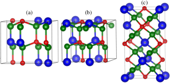
We obtain relaxed atomic structure and total energy of GaBP2 in three different phases (i.e. KT, ST and CP (see Fig.4)). Comparison of their formation enthalpy () using Eqn. 4 suggests KT and CP phases are more energetically favourable than ST phase.
| (4) |
where is the total energy of formula unit cell of and represent the chemical potential of element (For details see section IV of SI). The negative value of (see Table 1) suggests that the material can be synthesized at thermal equilibrium conditions.
IV.1.1 KT Phase

The DFT-PBE optimized lattice constant for GaBP2 are = 6.07 Å, b = 7.13 Å and c = 5.85 Å and = = = 90∘ is noted. The unit cell contains 16 atoms. At the basal plane Ga-P bond-length is 2.36-2.39 Å while axial bond is 2.38 Å long. Similarly, the planar and axial bond of B-P is 2.00 Å and 2.02 Å long respectively. We note the unit cell volume to be 253.5 Å3. Electronic structure obtained with DFT-PBE revealed a direct Eg of 0.97 eV at point (see section V of SI for band and dos plot). Atom and orbital projected densities of states (DOS) further revealed that the valence band (VB) is dominated by -orbital of P, a small contribution form -orbitals of Ga and B with a minute contribution from -orbital of P and Ga. -orbital of B appears at -5.0 eV below valence band maximum (VBM). The conduction band (CB) of the electronic structure is majorly contributed by Ga-, Ga-, B-, P-, and P- orbitals. A small contribution from Ga- and B- orbital is also noted ( see Fig. S2 (a) of SI).
It is well known to the literature that DFT-PBE severely underestimate Eg of materials. To overcome this issue various scheme has been proposed in past Morales-Garcia et al. (2017). In, recent times it was suggested that use of mBJ correction to the local/semi-local functional (such as LDA or GGA) can results in an estimation of accurate electronic Eg Chan and Ceder (2010). Nevertheless, use of hybrid functional (such as HSE06) along with DFT-PBE is now considered to be a gold standard for ab-initio estimation of Eg Garza and Scuseria (2016); Nguimdo and Joubert (2015). Here we used both functional to calculate Eg of materials. We found that the calculated Eg of GaBP2 in KT phase using mBJ and HSE06 functional is 1.50 and 1.65 respectively (see Table 1) close to our ML prediction. We present the HSE06 band-dispersion of GaBP2 around point in Fig.5 (a) where a direct Eg at point is noted. A full DFT-PBE band-dispersion relation is presented in Fig. S1(a) in SI. This direct Eg would allow for efficient absorption of the incident photon and hence a better PV efficiency.
IV.1.2 CP Phase
The optimized unit cell lattice constant of GaBP2 in CP phase are =b=c=6.07 Å and = = 130.44∘ and = 72.70 ∘. Here, unit cell contains 8 atoms and volume of the unit cell is noted as 126.56 . While the Ga-P bond is 2.37 Å long, the B-P bond-length is 2.01 Å. Electronic structure computed with DFT-PBE shows an in-direct Eg of 0.95 eV along -Z point. While the valence band maximum (VBM) is at [(0,0,0)] point, conduction band minimum (CBM) is at (, , ) k-point, where are the reciprocal lattice vector. DOS analysis suggest that the VB is dominated by p-orbital of P with a contribution from -orbitals of B and Ga. The CB is dominated by the -orbital of P and , , and -orbital of Ga and -orbital of B (see Fig. S2(b) in SI). We find a bit smaller Eg in CP phase in comparison to KT phase using HSE06 functional. We note an indirect Eg of 1.63 eV ( see Fig. 5 (b)).
Thus, our electronic structure analysis suggests that GaBP2 in KT-phase is most suitable for PV applications.
IV.2 Dynamical stability, Free energy and Mechanical stability

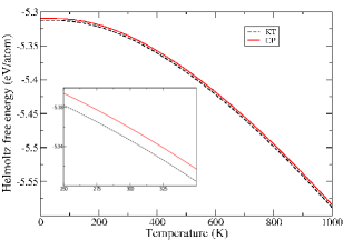
Further, we studied the dynamical stability of both KT and CP phase using DFPT simulation. We used phonopy code Togo and Tanaka (2015) where a supercell was used for simulation of phonon dispersion. Absence of any imaginary modes (see Fig.6 (a) and (b)) in both structure confirmed that GaBP2 can be synthesized in both phases. We estimated Helmholtz Free energy (A) as a function of temperature (T) of both configurations using the following relation:
| (5) |
Where and are the DFT free energy and vibrational free energy respectively. The is calculated as Togo and Tanaka (2015):
| (6) |
where and are the absolute temperature and the Boltzmann constant, respectively. is the Planck’s constant and is the frequency of the vibration of phonon mode. and are phonon wave vector and index of the band respectively. Our estimated suggests that in all temperature region, the KT phase is more stable than the CP phase, but with a relatively small difference of around 3 meV at 300K.
We evaluate the mechanical stability by using the Born criteria Mouhat and Coudert (2014). For KT phase which belongs to the orthorhombic crystal system, the necessary criteria are given as;
-
1.
-
2.
-
3.
-
4.
-
5.
-
6.
while for the CP phase which belongs to the tetragonal crystal system, the criteria are;
-
1.
-
2.
-
3.
-
4.
-
5.
.
Coefficient obtained with DFT-PBE satisfied all of the above mentioned criteria, which suggest GaBP2 is mechanically stable in both KT and CP phases. We have listed all the coefficient of stiff tensor in section VI of SI. We list other parameters corresponding to mechanical properties along with structural and electronic ones, of both phases in Table 2.
| Parameters | KT-Phase | CP-Phase |
| 11.95 | 12.10 | |
| 10.76 | 10.84 | |
| ED (eV) | 8.55 | 10 |
| Eg (eV) | 0.97(PBE), 1.65 (HSE) | 0.95(PBE), 1.63 (HSE) |
| (THz) | 21.02 | 20.25 |
| 22.43 | 22.51 | |
| 8.38 | 8.42 | |
| P | 0.02 | 0.02 |
| 3.73 | 3.74 | |
| K | 11.255 | 11.287 |
| G | 8.378 | 8.419 |
| Y | 20.137 | 20.226 |
| 0.202 | 0.201 |
= low frequency dielectric constant, = high frequency dielectric constant, ED = acoustic deformation potential, = Polar optical phonon frequency for the longitudinal mode, = longitudinal elastic constant, = transverse elastic constant, P = dimensionless piezoelectric coefficient, = density, K = Bulk modulus, G = Shear modulus, Y = Young modulus, = poisson’s ratio
IV.3 Electronic Transport
In addition to electronic structure, we calculated the mobility of n-type GaBP2 in both KT and CP phase using AMMCR code Mandia et al. (2019a). In our transport calculations, we included four scattering mechanisms viz. (i) ionized impurity, (ii) polar optical phonon (POP), (iii) acoustic deformation potential and (iv) piezoelectric scattering. It is worth mentioning here that at 300K, POP scattering has a significant influence on the transport properties of the III-V semiconductors. The fact that POP scattering is inelastic and anisotropic, makes relaxation time approximation inappropriate Rode (1975) for calculation the semi-classical transport properties of the III-V semiconductors. In this work, we solved the Boltzmann transport equation (BTE) using Rode’s iterative method Rode (1975) in order to obtain the perturbation in the electron distribution function due to different scattering mechanisms. Input parameters required for transport calculation viz. bandgap, optical phonon frequency, low and high frequency dielectric constants, dimensionless piezoelectric coefficient, the group velocity of the electron in the conduction band, elastic constants etc. are computed using DFT-PBE/DFPT-PBE and are tabulated in Table 2. Details of the methodology of our transport calculations are discussed in references Mandia et al., 2019b; Faghaninia et al., 2015. In KT phase the electron mobility is relatively higher compared to the CP phase thereby making the KT-GaBP2 more suitable for PVs and other optoelectronic applications. At 300K the estimated mobility of the KT and CP phases with a donor concentration of 1017 cm-3 is 1340 and 960 , respectively. For temperature (T) dependence of mobility in KT phase refer to section VII of SI. We note that in the T range of 150-700K, mobility decreases with increase in T while in low temperature region (50-150K) it increases with the increase in T (see Fig. S3 of SI).
Thus, our analysis from the ab-initio simulations suggests that GaBP2 is most stable in KT phase with a direct Eg of 1.65 eV, an excellent condition for the fabrication of high efficient PV solar cell. Negative formation enthalpy, dynamical and mechanical stability analysis together suggest that GaBP2 can be chemically synthesizable and is stable in KT phase. We find that energetic and properties of CP phase are very similar to the KT phase except the nature of the electronic Eg.
V Conclusion
In conclusion, we designed machine learning models to predict the bandgap of ternary II-IV-V and III-V semiconductors in ABX2 phase using a small and freely accessible dataset. The estimated RMSEs in predicting Eg is less than 0.4 eV. We obtained a set of numerical scaling laws for estimation of Eg using the unit cell volume as a single feature, which further concludes the compositional clustering of data between nitrides and non-nitrides. We filtered a new III-III-V2 semiconducting material with the chemical composition of GaBP2 which is suitable for PV applications. We predicted the electronic bandgap of GaBP2 and others using ML and validate them using ab-initio numerical simulations with mBJ and HSE06 functional. We studied the structural and electronic properties, and their thermal, dynamical and mechanical stability and concluded that the newly discovered material is stable. The estimated electron mobility of the GaBP2 is very similar to that of Si. The elemental earth abundance of the constituent elements, the electronic bandgap and electron mobility value along with a stable structural phase clearly suggest GaBP2 will be a next generation material for photovoltaic applications.
Data Availability Statement
The data that support the finding of this study are available from corresponding author upon reasonable request.
author contribution
UK and SN conceived the idea and contribute equally in the the machine learning and DFT part of the calculation. SC carried out the transport calculations. SN and UK wrote the mansucript and read by all authors. SB and S-C. L supervised the project.
Conflicts of Interest
There are no conflicts to declare.
References
- Shockley and Queisser (1961) W. Shockley and H. J. Queisser, Journal of Applied Physics 32, 510 (1961).
- Miller et al. (2012) O. D. Miller, E. Yablonovitch, and S. R. Kurtz, IEEE Journal of Photovoltaics 2, 303 (2012).
- Grätzel (2001) M. Grätzel, Nature 414, 338 (2001).
- Priolo et al. (2014) F. Priolo, T. Gregorkiewicz, M. Galli, and T. F. Krauss, Nature Nanotechnology 9, 19 (2014).
- Green (2009) M. A. Green, Progress in Photovoltaics: Research and Applications 17, 183 (2009).
- Curtarolo et al. (2013) S. Curtarolo, G. L. Hart, M. B. Nardelli, N. Mingo, S. Sanvito, and O. Levy, Nature Materials 12, 191 (2013).
- Greenu et al. (2015) M. Greenu, K. Emery, Y. Hishikawa, W. Warta, and E. Dunlop, Progress in Photovoltaics: Research and Applications 23, 805 (2015).
- Singh and Ravindra (2012) P. Singh and N. M. Ravindra, Solar Energy Materials and Solar Cells 101, 36 (2012).
- Wesoff (2016) E. Wesoff, Green Tech Media (PV Modules) (2016).
- Peters and Buonassisi (2018) I. M. Peters and T. Buonassisi, Joule 2, 1160 (2018).
- Wang et al. (2019) R. Wang, M. Mujahid, Y. Duan, Z.-K. Wang, J. Xue, and Y. Yang, Advanced Functional Materials , 1808843 (2019).
- Meng et al. (2018) L. Meng, J. You, and Y. Yang, Nature Communications 9, 5265 (2018).
- Lahourcade et al. (2013) L. Lahourcade, N. C. Coronel, K. T. Delaney, S. K. Shukla, N. A. Spaldin, and H. A. Atwater, Advanced Materials 25, 2562 (2013).
- Senabulya et al. (2016) N. Senabulya, N. Feldberg, R. A. Makin, Y. Yang, G. Shi, C. M. Jones, E. Kioupakis, J. Mathis, R. Clarke, and S. M. Durbin, AIP Advances 6, 075019 (2016).
- Feldberg et al. (2013) N. Feldberg, J. Aldous, W. Linhart, L. Phillips, K. Durose, P. Stampe, R. Kennedy, D. Scanlon, G. Vardar, R. Field III, et al., Applied Physics Letters 103, 042109 (2013).
- Skachkov et al. (2016) D. Skachkov, P. C. Quayle, K. Kash, and W. R. Lambrecht, Physical Review B 94, 205201 (2016).
- Zakutayev et al. (2014) A. Zakutayev, A. J. Allen, X. Zhang, J. Vidal, Z. Cui, S. Lany, M. Yang, F. J. DiSalvo, and D. S. Ginley, Chemistry of Materials 26, 4970 (2014).
- Wang et al. (2014) C. Wang, S. Chen, J.-H. Yang, L. Lang, H.-J. Xiang, X.-G. Gong, A. Walsh, and S.-H. Wei, Chemistry of Materials 26, 3411 (2014).
- Fioretti et al. (2015) A. N. Fioretti, A. Zakutayev, H. Moutinho, C. Melamed, J. D. Perkins, A. G. Norman, M. Al-Jassim, E. S. Toberer, and A. C. Tamboli, Journal of Materials Chemistry C 3, 11017 (2015).
- Martinez et al. (2016) A. D. Martinez, E. L. Warren, P. Gorai, K. A. Borup, D. Kuciauskas, P. C. Dippo, B. R. Ortiz, R. T. Macaluso, S. D. Nguyen, A. L. Greenaway, et al., Energy & Environmental Science 9, 1031 (2016).
- Narang et al. (2014) P. Narang, S. Chen, N. C. Coronel, S. Gul, J. Yano, L.-W. Wang, N. S. Lewis, and H. A. Atwater, Advanced Materials 26, 1235 (2014).
- Pandey et al. (2017) M. Pandey, K. Kuhar, and K. W. Jacobsen, The Journal of Physical Chemistry C 121, 17780 (2017).
- Tang et al. (2015) F. Tang, T. Zhu, F. Oehler, W. Y. Fu, J. T. Griffiths, F. C.-P. Massabuau, M. J. Kappers, T. L. Martin, P. A. Bagot, M. P. Moody, et al., Applied Physics Letters 106, 072104 (2015).
- Lee et al. (2018) J. K. Lee, B. Park, K. Song, W. Y. Jung, D. Tyutyunnikov, T. Yang, C. T. Koch, C. G. Park, P. A. van Aken, Y.-M. Kim, et al., Acta Materialia 145, 109 (2018).
- Reyes et al. (2013) D. F. Reyes, D. Gonzalez, F. Bastiman, L. Dominguez, C. J. Hunter, E. Guerrero, M. A. Roldan, A. Mayoral, J. P. David, and D. L. Sales, Applied Physics Express 6, 042103 (2013).
- Martini et al. (2003) S. Martini, A. Quivy, T. Lamas, M. Da Silva, E. Da Silva, and J. Leite, Journal of Crystal Growth 251, 101 (2003).
- Barlow et al. (2018) A. J. Barlow, N. Sano, B. J. Murdoch, J. F. Portoles, P. J. Pigram, and P. J. Cumpson, Applied Surface Science 459, 678 (2018).
- Mannarino et al. (2015) M. Mannarino, R. Chintala, A. Moussa, C. Merckling, P. Eyben, K. Paredis, and W. Vandervorst, Journal of Applied Physics 118, 225304 (2015).
- Scanlon and Walsh (2012) D. O. Scanlon and A. Walsh, Applied Physics Letters 100, 251911 (2012).
- Gautam et al. (2015) R. Gautam, P. Singh, S. Sharma, S. Kumari, and A. Verma, Materials Science in Semiconductor Processing 40, 727 (2015).
- Butler et al. (2018) K. T. Butler, D. W. Davies, H. Cartwright, O. Isayev, and A. Walsh, Nature 559, 547 (2018).
- Sparks et al. (2016) T. D. Sparks, M. W. Gaultois, A. Oliynyk, J. Brgoch, and B. Meredig, Scripta Materialia 111, 10 (2016).
- Xue et al. (2017) D. Xue, D. Xue, R. Yuan, Y. Zhou, P. V. Balachandran, X. Ding, J. Sun, and T. Lookman, Acta Materialia 125, 532 (2017).
- De Jong et al. (2016) M. De Jong, W. Chen, R. Notestine, K. Persson, G. Ceder, A. Jain, M. Asta, and A. Gamst, Scientific Reports 6, 34256 (2016).
- Zheng et al. (2018) X. Zheng, P. Zheng, and R.-Z. Zhang, Chemical Science 9, 8426 (2018).
- Pilania et al. (2013) G. Pilania, C. Wang, X. Jiang, S. Rajasekaran, and R. Ramprasad, Scientific Reports 3, 2810 (2013).
- Goodman (1957) C. Goodman, Nature 179, 828 (1957).
- Jaffe and Zunger (1984) J. Jaffe and A. Zunger, Physical Review B 29, 1882 (1984).
- F et al. (2011) P. F, V. G, M. V. Gramfort A, T. B, B. M. Grisel O, P. P, W. R, D. V, and V. J, Journal of Machine Learning Research 12, 2825 (2011).
- Chen and Guestrin (2016) T. Chen and C. Guestrin, in Proceedings of the 22nd acm sigkdd international conference on knowledge discovery and data mining (ACM, 2016) pp. 785–794.
- Kresse and Furthmüller (1996a) G. Kresse and J. Furthmüller, Computational Materials Science 6, 15 (1996a).
- Kresse and Furthmüller (1996b) G. Kresse and J. Furthmüller, Physical Review B 54, 11169 (1996b).
- Kresse and Joubert (1999) G. Kresse and D. Joubert, Physical Review B 59, 1758 (1999).
- Perdew et al. (1996) J. P. Perdew, K. Burke, and M. Ernzerhof, Physical Review Letters 77, 3865 (1996).
- Monkhorst and Pack (1976) H. J. Monkhorst and J. D. Pack, Physical Review B 13, 5188 (1976).
- Becke and Johnson (2006) A. D. Becke and E. R. Johnson, The Journal of Chemical Physics 124, 221101 (2006).
- Heyd et al. (2005) J. Heyd, J. E. Peralta, G. E. Scuseria, and R. L. Martin, The Journal of Chemical Physics 123, 174101 (2005).
- Mandia et al. (2019a) A. K. Mandia, B. Muralidharan, J.-H. Choi, S.-C. Lee, and S. Bhattacharjee, arXiv preprint arXiv:1907.08005 (2019a).
- Huang et al. (2019) Y. Huang, C. Yu, W. Chen, Y. Liu, C. Li, C. Niu, F. Wang, and Y. Jia, Journal of Materials Chemistry C 7, 3238 (2019).
- Rajan et al. (2018) A. C. Rajan, A. Mishra, S. Satsangi, R. Vaish, H. Mizuseki, K.-R. Lee, and A. K. Singh, Chemistry of Materials 30, 4031 (2018).
- (51) B. Olsthoorn, R. M. Geilhufe, S. S. Borysov, and A. V. Balatsky, Advanced Quantum Technologies 0, 1900023, https://onlinelibrary.wiley.com/doi/pdf/10.1002/qute.201900023 .
- Sotskov et al. (2018) V. Sotskov et al., “Band gap prediction for inorganic crystals with machine learning, master thesis,” (2018).
- Dalven (1973) R. Dalven, Phys. Rev. B 8, 6033 (1973).
- Morales-Garcia et al. (2017) A. Morales-Garcia, R. Valero, and F. Illas, The Journal of Physical Chemistry C 121, 18862 (2017).
- Chan and Ceder (2010) M. Chan and G. Ceder, Physical Review Letters 105, 196403 (2010).
- Garza and Scuseria (2016) A. J. Garza and G. E. Scuseria, The Journal of Physical Chemistry Letters 7, 4165 (2016).
- Nguimdo and Joubert (2015) G. D. Nguimdo and D. P. Joubert, The European Physical Journal B 88, 113 (2015).
- Togo and Tanaka (2015) A. Togo and I. Tanaka, Scripta Materialia 108, 1 (2015).
- Mouhat and Coudert (2014) F. Mouhat and F.-X. Coudert, Physical Review B 90, 224104 (2014).
- Rode (1975) D. Rode, in Semiconductors and Semimetals, Vol. 10 (Elsevier, 1975) pp. 1–89.
- Mandia et al. (2019b) A. K. Mandia, R. Patnaik, B. Muralidharan, S.-C. Lee, and S. Bhattacharjee, Journal of Physics: Condensed Matter 31, 345901 (2019b).
- Faghaninia et al. (2015) A. Faghaninia, J. W. Ager III, and C. S. Lo, Physical Review B 91, 235123 (2015).