Hardware Design and Analysis of the ACE and WAGE Ciphers
Mark D. Aagaard, Marat Sattarov, and Nuša Zidarič
Department of Electrical and Computer Engineering
University of Waterloo, Ontario, Canada
{maagaard,msattaro,nzidaric}@uwaterloo.ca
Abstract
This paper presents the hardware design and analysis of ACE and WAGE, two candidate ciphers for the NIST Lightweight Cryptography standardization. Both ciphers use sLiSCP’s unified sponge duplex mode. ACE has an internal state of 320 bits, uses three 64 bit Simeck boxes, and implements both authenticated encryption and hashing. WAGE is based on the Welch-Gong stream cipher and provides authenticated encryption. WAGE has 259 bits of state, two 7 bit Welch-Gong permutations, and four lightweight 7 bit S-boxes. ACE and WAGE have the same external interface and follow the same I/O protocol to transition between phases. The paper illustrates how the ACE and WAGE algorithms were translated into hardware and some of the key design decisions in this process. The paper reports area, power, and energy results for both serial and parallel (unrolled) implementations using four different ASIC libraries: two 65 nm libraries, a 90 nm library, and a 130 nm library. ACE implementations range from a throughput of 0.5 bits-per-clock cycle (bpc) and an area of 4210 GE (averaged across the four ASIC libraries) up to 4 bpc and 7260 GE. WAGE results range from 0.57 bpc with 2920 GE to 4.57 bpc with 11080 GE.
1 Introduction
In 2013, NIST started the Lightweight Cryptography (LWC) project [1], with the end goal of creating a portfolio of lightweight algorithms for authenticated encryption with associated data (AEAD), and optionally hashing, in constrained environments [2]. For hardware-oriented lightweight algorithms, hardware implementation results are an important criteria for assessment and comparison. In the first round of the LWC evaluation, more than half of the candidates [3] reported hardware implementation results or their estimates, ranging from complete implementation and analysis to partial implementation results and theoretical estimates based on gate count. Various amounts of analysis, such as area reported only for a cryptographic primitive used or thorough area breakdown of all components, different design decisions, such as serial and unrolled implementations, and different ASIC and/or FPGA implementation technologies can be found. Furthermore, some authors report the results without interface, some with the interface, and in some cases, e.g. [6], CAESAR Hardware Applications Programming Interface (API) for Authenticated Ciphers [7] was used. This paper describes how the algorithms for ACE [4] and WAGE [5], two LWC candidates, were translated into hardware implementations; the parallel (unrolled) implementations; and implementation results for four ASIC libraries.
Section 2 describes the ACE and WAGE permutations and the sLiSCP sponge duplex mode [9] that define the ACE and WAGE algorithms as specified in the ACE and WAGE LWC submissions [4, 5] and which represents work done by the entire ACE and WAGE teams. Section 3 explores how the permutation and mode were combined together into efficient implementations in hardware and analyzes some of the key design decisions in this process. Section 4 describes the parallel implementations of ACE and WAGE. Implementation technologies and results are summarized in Section 5. The implementations were synthesized using four different ASIC libraries, including 65 nm, 90 nm and 130 nm technologies. ACE implementations range from a throughput of 0.5 bits-per-clock cycle (bpc) and an area of 4210 GE (averaged across the four ASIC libraries) up to 4 bpc and 7260 GE. WAGE results range from 0.57 bpc with 2920 GE to 4.57 bpc with 11080 GE.
2 Background
This section describes the ACE and WAGE permutations and the sLiSCP unified duplex sponge mode as specified in the NIST LWC competition submissions [4, 5]. Both ACE and WAGE permutations operate in a unified duplex sponge mode [9]. The 320 bit ACE permutation offers both AEAD and hashing functionalities, and the 259 bit WAGE permutation supports AEAD functionality. Because of the similarities between ACE and WAGE, this section begins with a short description of ACE and WAGE permutations, followed by a discussion on the unified duplex sponge mode for both schemes, highlighting some differences.
2.1 ACE Permutation
ACE has a 320 bit internal state, divided into five 64 bit registers, denoted A, B, C, D, and E. The ACE permutation consists of 16 steps (Figure 1), each of which consists of 8 rounds. ACE uses the unkeyed reduced-round Simeck block cipher [10] with a block size of 64, denoted Simeck box for one round of the full 8-round S-box, as the nonlinear operation. is a lightweight permutation, consisting of left cyclic shifts, and and xor gates. Each round is parameterized by a single bit of a round constant.
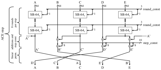
In each round, is applied to three registers A, C and E, with each using its own 1 bit round constant. The round constants are generated by a 7 bit LFSR run in a 3-way parallel configuration to produce one bit of each round constant per clock cycle.
In each step, the outputs of are added to registers B, D and E, which are further parameterized by 8 bit step constants . The computation of step constants does not need any extra circuitry, but rather uses the same LFSR as the round constants: the three feedback values together with all 7 state bits yield 10 consecutive sequence elements, which are then split into three 8 bit step constants. The step constants are used once every 8 clock cycles. The step function is then concluded by a permutation of all five registers. For the properties of , the choice of the final permutation, and the number of rounds and steps refer to [4].
2.2 WAGE Permutation
WG is a hardware oriented scheme, built on top of the initialization phase of the well-studied, LFSR based, Welch-Gong (WG) stream cipher [11, 12]. The WAGE permutation is iterative and has a round function derived from the LFSR, the decimated Welch-Gong permutation WGP, and small S-boxes SB. Details, such as differential uniformity and nonlinearity of the WGP and SB and selection of the LFSR polynomial can be found in [5].
Both LFSR and WGP are defined over and the S-box is a 7 bit permutation. The LFSR is defined by the feedback polynomial , which is primitive over . The 37 stages of the LFSR also constitute the internal state of WAGE.
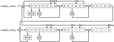
The WAGE permutation is iterative, and repeats its round function (Figure 2) 111 times. In each round, 6 stages of the LFSR are updated nonlinearly, while all the remaining stages are just shifted. A pair of 7 bit round constants is xored with the pair of stages . Round constants are produced by a 7 bit LFSR implemented in a 2-way parallel configuration.
2.3 The Unified Duplex Sponge Mode
ACE--128 and WAGE--128 use the unified duplex sponge mode from sLiSCP [9] (Figure 3). The phases for encryption and decryption are: initialization, processing of associated data, encryption (Figure 3(a)) or decryption (Figure 3(b)), and finalization. Figure 3 also shows the domain separators for each phase. The internal state is divided into a capacity part (256 bits for ACE--128 and 195 bits for WAGE) and a 64 bit rate , which for:
-
•
ACE--128 consists of bytes A[7], A[6], A[5], A[4], C[7], C[6], C[5], C[4]
-
•
WAGE--128 consists of the 0-th bit of stage (i.e., ) and all bits of stages , and
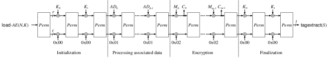
The input data (associated data , message or ciphertext ) is absorbed (or replaced) into the rate part of the internal state. If the input data length is not a multiple of 64, padding with (10∗) is needed. In Figure 3, denotes the number of 64 bit blocks of and the number of 64 bit blocks of and after padding. Refer to [4, 5] for further padding rules. No padding is needed during initialization and finalization because the key, nonce, and IV are all 128 bits, which is exactly 2 blocks. With the exception of tag extraction, both schemes generate an output only during the encryption and decryption phases: the 64 bit output block is obtained by the xor of the current input and rate.
The loading and tag-extraction functions are straightforward for ACE, but more complicated for WAGE. For ACE, the key is loaded into registers A and C, the nonce into B and E, and the register D is loaded with zeros. The ACE extracts the 128 bit tag from registers A and C. For WAGE, the loading and tag extraction functions were designed to take advantage of the shifting nature of the LFSR, which will be discussed in more detail in Section 3.3.
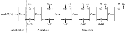
The ACE HASH functionality is shown in Figure 4. The only input is the message . Since the hash has a fixed length of 256 bits, the length of the squeezing phase is fixed. ACE--256 is unkeyed, and the state is loaded with a fixed initialization vector IV. More specifically, the function loads the state bytes B[7], B[6] and B[5] with bytes 0x80, 0x40, and 0x40 respectively, and sets all other state bits to zero.
3 Hardware Implementations
This section describes and analyses the hardware implementations of ACE and WAGE. The next section describes the parallel implementations, followed by results in Section 5. Section 3.1 summarizes the principles underlying the hardware design and the interfaces for the ciphers. Sections 3.2 and 3.3 describe ACE and WAGE. Section 3.4 summarizes some of the key hardware-oriented design decisions.
3.1 Hardware Design Principles and Interface with the Environment
-
1.
Multi-functionality module. The system should include all supported operations in a single module (Figure 6), because lightweight applications cannot afford the extra area for separate modules.
-
2.
Single input/output ports. In small devices, ports can be expensive. To ensure that ACE and WAGE are not biased in favour of the system, at the expense of the environment, the ciphers have one input and one output port (Table 3.1). That being said, the authors agree with the proposed lightweight cryptography hardware API’s [8] use of separate public and private data ports and will update implementations accordingly.
-
3.
Valid-bit protocol and stalling capability. The environment may take an arbitrarily long time to produce any piece of data. For example, a small microprocessor could require multiple clock cycles to read data from memory and write it to the system’s input port. The receiving entity must capture the data in a single clock cycle (Figure 6). In reality, the environment can stall as well. In the future, ACE and WAGE implementations will be updated to match the proposed lightweight cryptographic hardware API’s use of a valid/ready protocol for both input and output ports.
-
4.
Use a “pure register-transfer-level” implementation style. In particular, use only registers, not latches; multiplexers, not tri-state buffers; synchronous, not asynchronous reset; no scan-cell flip-flops; clock-gating is used for power and area optimization.
Since both ACE and WAGE use a unified sponge duplex mode, they share a common interface with the environment (Table 3.1). The environment separates the associated data and the message/ciphertext, and performs padding if necessary. The domain separators shown in Figure 3 are provided by the environment and serve as an indication of the phase change for AEAD functionality. For ACE--256, the phase change is indicated by the change of the i_mode(0) signal, as shown in Table 2. The hardware is unaware of the lengths of individual phases, hence no internal counters for the number of processed blocks are needed.
| Input signal | Meaning |
|---|---|
| reset | resets the state machine |
| i_mode | mode of operation |
| i_dom_sep | domain separator |
| i_padding | the last block is padded |
| i_data | input data |
| i_valid | valid data on i_data |
| Output signal | Meaning |
| o_ready | hardware is ready |
| o_data | output data |
| o_valid | valid data on o_data |
| i_mode | |||
| (1) | (0) | Mode | Operation or phase |
| 0 | 0 | ACE- | Encryption |
| 0 | 1 | ACE- | Decryption |
| 1 | 0 | ACE--256 | Absorb |
| 1 | 1 | ACE--256 | Squeeze |
| - | 0 | WAGE- | Encryption |
| - | 1 | WAGE- | Decryption |
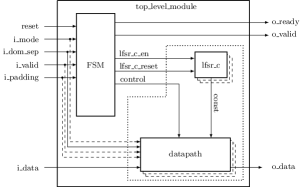
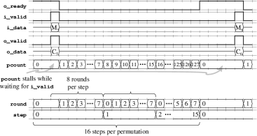
The top-level module, shown in Figure 6, is also very similar for both ACE and WAGE. It depicts the interface signals from Table 3.1, with only slight differences in bitwidths. Figure 6 shows the timing diagram for ACE during the encryption phase of message blocks and , which clearly shows the valid-bit protocol. The first five lines show the top-level interface signals and line six shows the value of the permutation counter pcount, which is a part of the ACE finite state machine (FSM) and keeps track of the clock cycles needed for one ACE permutation. After completing the previous permutation, the top-level module asserts o_ready to signal to the environment that an ACE permutation just finished and new data can be accepted. The environment replies with a new message block accompanied by an i_valid signal. The hardware immediately encrypts, returns and asserts o_valid. This clock cycle is also the first round of a new ACE permutation and the o_ready is deasserted, indicating that the hardware is busy. Figure 6 shows the ACE hardware remaining busy (o_ready = 0) for the duration of one ACE permutation. When pcount wraps around from 127 to 0, the hardware is again idle and ready to receive new input, in this case . A few more details about the use of pcount will follow in Subsection 3.2. The interaction between the top-level module and the environment during the encryption phase of WAGE is very similar, with 111 clock cycles for the completion of one permutation. More significant differences for the interaction with the environment arise during loading, tag extract and of course ACE--256.
3.2 ACE Datapath
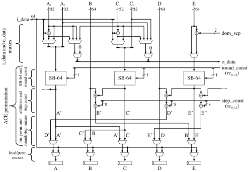
Figure 7(a) shows the ACE datapath. The top and bottom of the figure depict the five 64 bit registers A, B, C, D and E.
The support for the different phases in the mode (e.g., load, initialization, encryption, etc.) imposes a variety of multiplexers onto the core datapath for performing the round computation. The multiplexers are controlled by the mode and the counter pcount. Near the top of Figure 7(a), are multiplexers to determine the input to the round function and the data that is sent to the output. Next, the output multiplexers are needed to accommodate encryption/decryption and tag generation for ACE--128 and squeezing for ACE--256. Furthermore, the output is forced to 0 during normal operation. The middle of the figure includes for the round function. Below is the hardware for the step function: xor gates for the addition and step constant and the linear permutation. The first row of multiplexers at the bottom is to select between doing a round vs. step; the bottom row is to select between loading (key, nonce, IV) or doing a normal (round, step, permutation) computation.

3.3 WAGE Datapath
Because of the shifting nature of the LFSR, which in turn affects loading, absorbing and squeezing, the WAGE datapath is slightly more complicated than the ACE datapath and hence is explained in two levels:
-
1.
Implementation of the permutation
-
•
WGP module implementing WGP: For smaller fields like , the WGP area, when implemented as a constant array in VHDL/Verilog (i.e., as a look-up table) is smaller than when implemented using components such as multiplication and exponentiation to powers of two [13, 14]. However, the WGP is not implemented in hardware as a memory array, but rather as a net of and, or, xor and not gates, derived and optimized by the synthesis tools.
-
•
SB module: The function is defined as 5 iterations of smaller functions, but is implemented in unrolled fashion, (i.e., as purely combinational logic).
-
•
lfsr_c: The lfsr_c for generating the round constants was implemented in a 2-way parallel fashion. It has only 7 1 bit stages and two xor gates for the two feedback computations.
-
•
-
2.
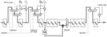
Support for the sponge mode. Figure 8 shows details for stages . The grey line represents the path for normal operation during the WAGE permutation. The additional hardware for the entire wage_lfsr is listed below, with examples in brackets referring to Figure 8.
-
•
The 64 bit i_data is padded with zeros to 70 bits, then fragmented into 7 bit wage_lfsr inputs , , corresponding to the rate stages . For each data input there is a corresponding 7 bit data output . ( and in Figure 8).
-
•
10 xor gates must be added to the stages to accommodate absorbing, encryption and decryption (xors at stages ,).
-
•
10 multiplexers to switch between absorbing and normal operation (Amux1, Amux0 at ,).
-
•
An xor and a multiplexer are needed to add the domain separator i_dom_sep (Amux at ).
-
•
To replace the contents of the stages, 10 multiplexers are added (Rmux1 at stage )
-
•
Instead of additional multiplexers for loading, the existing Rmux, , multiplexers are now controlled by replace or load and labelled RLmux, (see RLmux0 on ). Since all non-input stages must keep their previous values, an enable signal lfsr_en is needed.
-
•
Three 7 bit and gates to turn off the inputs and (and at ).
-
•
Four multiplexers are needed to turn off the SB during loading and tag extraction (SBmux at ).
-
•
The total hardware cost to support the sponge mode is: 24 7 bit and one 2 bit multiplexers, 10 7 bit and one 2 bit xor gates, three 7 bit and gates.
-
•
As mentioned in Section 2, special care was given to the design of loading and tag-extract. The existing data inputs are reused for loading, and the outputs for tag extraction. The wage_lfsr is divided into five loading regions using the inputs , . For example, the region in Figure 8 is loaded through input , however, instead of storing , the data is fed directly into , i.e., the RLmux0 disconnects the Amux0 output. The remaining stages in this region are loaded by shifting, which requires the SBmux at . Note that there is no need to disconnect the two WGP, because they are automatically disabled by loading through and , located at stages and respectively. The tag is extracted in a similar fashion as loading, but from the data output at the end of a particular loading region, e.g., the region , loaded through , is extracted through . The longest tag extraction region is of length 9, which is the same as the longest loading region.
3.4 Hardware-Oriented Design Decisions and Analysis
The design process for ACE and WAGE tightly integrated cryptanalysis and hardware optimizations. A few key hardware-oriented decisions are highlighted here; more can be found in the design rationale chapters of [4, 5].
Functionally, it is equivalent for the boundary between phases to occur either before or after the permutation. For ACE and WAGE, the boundary was placed after the permutation updates the state register. This means that the two-bit domain separator is sufficient to determine the value of many of the multiplexer select lines and other control signals. All phases that have a domain separator of "00" have the same multiplexer select values. The same also holds true for "01". Unfortunately, this cannot be achieved for "10", because encryption and decryption require different control signal values, but the same domain separator. Using the domain separator to signal the transition between phases for encryption and decryption also simplifies the control circuit. For hashing, the change in phase is indicated by the i_mode signal.
In applications where the delay through combinational circuitry is not a concern, such as with lightweight cryptography, where clock speed is limited by power consumption, not by the delay through combinational circuitry, it is beneficial to lump as much combinational circuitry as possible together into a single clock cycle. This provides more optimization opportunities for the synthesis tools than if the circuitry was separated by registers. For this reason, the ACE datapath was designed so that the input and output multiplexers, one round of the permutation, and state loading multiplexers together form a purely combinational circuit, followed by the state register.
Figure 9 shows the area analysis and comparison for ACE and WAGE. The coloured columns show the estimated area for different components based on counting gates from the mathematical definitions. The grey columns show the actual area from logical synthesis using a compilation script with minimal optimizations so as to preserve structural hierarchy. Table 3 shows the final results with optimized synthesis scripts and after physical synthesis (post place-and-route). Figure 9 shows that ACE and WAGE have relatively similar area for the permutation with multiplexers: 2143 GE for ACE and 1984 GE for WAGE, making ACE 8% larger. The larger area of ACE is due mostly to the large number of multiplexers used to support the mode and input/output.
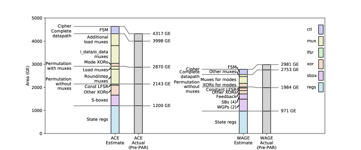
The synthesized area of ACE is less than the estimated area, while the opposite is true for WAGE. As can be seen in comparing Figures 7 and 8, the WAGE datapath is distributed into a large number of small lumps separated by registers, while the ACE datapath is relatively monolithic, which gives the synthesis tools more opportunities for optimizations.
4 Parallel Implementations
4.1 Parallelization in General
Both ciphers can be parallelized (unrolled) to execute multiple rounds per clock cycle, at the cost of increased area. In the top-level schematic in Figure 6, the dashed stacked boxes indicate parallelization. The FSM is parameterized with parameter and used for un-parallelized () and parallelized () implementations. Other components are replicated to show copies, with in Figure 6. Such a representation is symbolic; parallelization is applied only to the permutation, not the entire datapath. The interface with the environment remains the same.
4.2 ACE
The un-parallelized ACE permutation performs a single round per clock cycle, which implies 8 clock cycles per step. Parallel (i.e., unrolled) versions perform rounds per clock cycle, and were implemented for divisors of 8 (i.e. ). The ACE permutation could be parallelized further, e.g. two or more steps in a single clock cycle. Figure 7(b) shows the example for registers A and B, with copies of connected in series. Each has its own round constant , . The round vs. step multiplexers are still needed, and can be removed only for values of , that are multiples of 8. Also note the step constant indicated as . For a step is concluded in 2 clock cycles. However, this requires a modification to the lfsr_c, which must now generate round constant bits , , per clock cycle. The last cycle within a step requires 7 additional bits, which together with yield 10 bits for the step constant generation . In the case the lfsr_c must generate 12 constant bits in the first cycle and 19 constant bits in the second clock cycle of the step, which are then used for and . For the extra constant bits, the lfsr_c feedback was replicated (i.e., feedbacks in addition to the original 3).
4.3 WAGE
WAGE performs one clock cycle for the interaction with the environment (i.e. absorbing or replacing the input data into the state) followed by 111 clock cycles of the WAGE permutation. Because 111 is divisible only by 3 and 37, the opportunities to parallelize WAGE appear rather limited. However, by treating the absorption or replacement of the input data into the internal state as an additional clock cycle in the permutation, we increase the the length of the permutation to 112 clock cycles. Because 112 has many divisors, this allows parallelism of . The cost is some additional multiplexers, because the clock cycle that loads data has different behaviour than the normal clock cycles
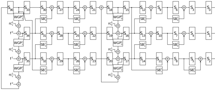
Figure 10 shows the 3-way parallel wage_lfsr including all nonlinear components and their copies. Multiplexers are not replicated, and hence, are not shown. For the components and SB in Figure 10, the superscript indicates the original () and the two copies (). Computation of the three feedbacks is not shown but is conducted as . Similar to ACE, the generation of WAGE round constants must be parallelized as well. For readability, the two WGP were labelled , with being the original WGPs positioned at , just like . Similarly, the SBs were also labelled , , in the decreasing order (i.e., is the original SB with input ).
5 Implementation Technologies and ASIC Implementation Results
Logic synthesis was performed with Synopsys Design Compiler version P-2019.03 using the compile_ultra command and clock gating. Physical synthesis (place and route) and power analysis were done with Cadence Encounter v14.13 using a density of 95%. simulations were done in Mentor Graphics ModelSim SE v10.5c. The ASIC cell libraries used were ST Microelectronics 65 nm CORE65LPLVT 1.25V, TSMC 65 nm tpfn65gpgv2od3 200c and tcbn65gplus 200a at 1.0V, ST Microelectronics 90 nm CORE90GPLVT and CORX90GPLVT at 1.0V, and IBM 130nm CMRF8SF LPVT with SAGE-X v2.0 standard cells at 1.2V. Some past works have used scan-cell flip-flops to reduce area, because these cells include a 2:1 multiplexer in the flip-flop which incurs less area than using a separate multiplexer. Scan-cell flip-flops were not used because their use as part of the design would prevent their insertion for fault-detection and hence, prevent the circuit from being tested for manufacturing faults. Furthermore, chip enable signals were removed from all datapath registers, which are controlled by clock gating instead. This allows a further reduction of the implementation area.
| Throughput is measured in bits per clock cycle (bpc), and plotted on a log scale axis. |
| The area axis is scaled as log(Area2). |
| ST Micro 65 nm | TSMC 65 nm | ST Micro 90 nm | IBM 130 nm | ||||||||||
| Label | Tput | A | f | E | A | f | E | A | f | E | A | f | E |
| [A/W-] | [bpc] | [GE] | [MHz] | [nJ] | [GE] | [MHz] | [nJ] | [GE] | [MHz] | [nJ] | [GE] | [MHz] | [nJ] |
| ACE | |||||||||||||
| A-1 | 0.5 | 4250 | 720 | 27.9 | 4600 | 705 | 20.1 | 3660 | 657 | 62.2 | 4350 | 128 | 46.8 |
| A-2 | 1 | 4780 | 618 | 18.4 | 5290 | 645 | 12.4 | 4130 | 628 | 35.8 | 4980 | 88.9 | 29.4 |
| A-4 | 2 | 5760 | 394 | 15.1 | 6260 | 588 | 8.51 | 4940 | 484 | 25.4 | 5910 | 90.5 | 21.1 |
| A-8 | 4 | 7240 | 246 | 11.4 | 8090 | 493 | 6.40 | 6170 | 336 | 19.4 | 7550 | 63.2 | 18.4 |
| WAGE | |||||||||||||
| W-1 | 0.57 | 2900 | 907 | 20.0 | 3290 | 1120 | 13.0 | 2540 | 940 | 39.2 | 2960 | 153 | 30.4 |
| W-2 | 1.14 | 4960 | 590 | 19.1 | 5310 | 693 | 10.6 | 4280 | 493 | 34.4 | 4850 | 98.5 | N/A†† |
| W-3 | 1.68 | 5480 | 397 | 20.4 | 5930 | 527 | 10.7 | 4770 | 414 | 31.2 | 5460 | 79.6 | 26.5 |
| W-4 | 2.29 | 6780 | 307 | 24.0 | 7460 | 387 | 12.1 | 5790 | 277 | 32.9 | 6700 | 51.9 | 33.4 |
| W-8 | 4.57 | 12150 | 192 | 38.5 | 11870 | 204 | 19.9 | 9330 | 137 | 49.9 | 10960 | 34.5 | 59.9 |
Note: Energy results done with timing simulation at 10 MHz.
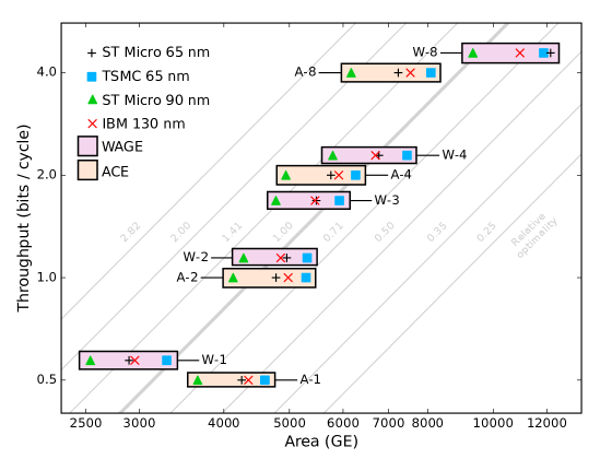
Figure 11 shows area2 vs. throughput for both ACE and WAGE with different degrees of parallelization, denoted by W- and A- (). The throughput axis is scaled as log(Tput) and the area axis is scaled as log. The grey contour lines denote the relative optimality of the circuits using Tput/area2. Throughput is increased by increasing the degree of parallelization (unrolling), which reduces the number of clock cycles per permutation round.
In comparing to the logic-synthesis with minimal optimization results in Figure 9, the area for ACE has decreased by 1.6% and the area for WAGE has decreased by 2.7%. As parallelization is increased, WAGE’s area grows faster than ACE’s. For ACE, only the S-boxes and a little bit of circuitry for the constant LFSR needs to be replicated (approximately 500 GE). WAGE requires the feedback, WGPs, and small SB S-boxes be replicated. The area increase is larger than that of ACE, and also less consistent. Going from to results in area increase for ACE and for WAGE on average. Optimality for WAGE reaches a maximum at . For ACE, optimality continues to increase beyond .
As can be seen by the relative constant size of the shaded rectangles enclosing the data points, the relative area increase with parallelization is relatively independent of implementation technology.
Table 3 represents the same data points as Figure 11 with the addition of maximum frequency (f, MHz) and energy per bit (E, nJ). Energy is measured as the average value while performing all cryptographic operations over 8192 bits of data at 10 MHz. As the ACE throughput increases, energy per bit decreases consistently, despite higher circuit area and, therefore, power consumption. However, this is not the case with WAGE. When unrolling a combinational circuit, glitches increase exponentially with circuit depth. The critical path in ACE’s S-box has only 2 gates, while the critical path in WAGE’s WGP contains 10 gates. The significantly longer critical path, combined with the larger overall area of WGP, cause energy consumption to increase with parallelization for WAGE.
Table 4 summarizes the area on ST Micro 65 nm of the LWC submissions[3] that included synthesizable VHDL or Verilog code. Table 4 reports the area results obtained using the ST Micro 65 nm process and tool flow from this paper and the results reported in the submission. The various ciphers use different protocols and interfaces, sometimes provide different functionality (e.g., with or without hashing), and use different key sizes. As such, this analysis is very imprecise, but gives a rough comparison to ACE and WAGE results. As the LWC competition progresses and the hardware API matures, more precise comparisons will become possible. This preliminary analysis indicates that ACE and WAGE are among the smaller cipher candidates.
| This work | Reported in submission documents [3] | |||
|---|---|---|---|---|
| Cipher | Module | Area (kGE) | Area (kGE) | ASIC technology used |
| Drygascon | drygascon128_1round_cycle |
29.6 | N/A | |
| Gage | gage1h256c224r008AllParallel |
10.4 | N/A | |
| Lilliput-AE | lilliputaei128v1 encryptdecrypt |
9.9 | 4.2 | theoretical estimate for 5 lanes |
| Remus | remus_top |
7.4 | 3.6 | TSMC 65nm |
| Subterranean | crypto_aead simple_axi4_lite |
6.5 | 5.7 | FreePDK 45nm |
| Triadx | triadx1 |
1.5 | ||
| Thash | thash1 |
1.5 | ||
6 Conclusion
The goal of the ACE and WAGE design process was to build on the well studied Simeck S-Box and Welch-Gong permutation. The overall algorithms were designed to lend themselves to efficient implementations in hardware and to scale well with increased parallelism. ACE has a larger internal state: 320 bits, vs 259 for WAGE, but the ACE permutation is smaller than that of WAGE. This means the non-parallel version of WAGE is smaller than that of ACE, but as parallelism increases, WAGE eventually becomes larger than ACE. At 1 and 2 bits-per-cycle, the designs are relatively similar in area. A number of the NIST LWC candidate ciphers provided synthesizable source code. A preliminary comparison with these ciphers on ST Micro 65 nm indicates that ACE and WAGE are likely to be among the smaller candidates.
Acknowledgements This work benefited the collaborative environment of the Communications Security (ComSec) Lab at the University of Waterloo, and in particular discussions with ACE and WAGE crypto team of Riham AlTawy, Guang Gong, Kalikinkar Mandal, and Raghvendra Rohit.
References
- [1] NIST Lightweight Cryptography https://csrc.nist.gov/Projects/Lightweight-Cryptography
- [2] Submission Requirements and Evaluation Criteria for the Lightweight Cryptography Standardization Process https://csrc.nist.gov/CSRC/media/Projects/Lightweight-Cryptography/documents/final-lwc-submission-requirements-august2018.pdf
- [3] NIST Lightweight Cryptography round 1 candidates https://csrc.nist.gov/Projects/Lightweight-Cryptography/Round-1-Candidates
- [4] M.D. Aagaard2, R. AlTawy1, G. Gong1, K. Mandal1, R. Rohit1. “ACE: An Authenticated Encryption and Hash Algorithm — Submission to the NIST LWC Competition”, March 2019, https://csrc.nist.gov/CSRC/media/Projects/Lightweight-Cryptography/documents/round-1/spec-doc/ace-spec.pdf (1: Hardware group, 2: Crypto group)
- [5] M.D. Aagaard2, R. AlTawy1, G. Gong1, K. Mandal1, R. Rohit1, N. Zidarič2. “WAGE: An Authenticated Cipher — Submission to the NIST LWC Competition”, March 2019, https://csrc.nist.gov/CSRC/media/Projects/Lightweight-Cryptography/documents/round-1/spec-doc/wage-spec.pdf (1: Hardware group, 2: Crypto group)
- [6] B. Rezvani, W. Diehl, “Hardware Implementations of NIST Lightweight Cryptographic Candidates: A First Look”, Cryptology ePrint Archive, Report 2019/824, 2019.
- [7] E. Homsirikamol, W. Diehl, A. Ferozpuri, F. Farahmand, P. Yalla, J.P. Kaps, K. Gaj, “CAESAR Hardware API.” Cryptology ePrint Archive, Report 2015/669, 2016.
- [8] J.P. Kaps, W. Diehl, M. Tempelmeier, E. Homsirikamol, K. Gaj, “Hardware API for Lightweight Cryptography”, 2019
- [9] R. AlTawy, R. Rohit, M. He, K. Mandal, G. Yang and G. Gong. sLiSCP: Simeck-based Permutations for Lightweight Sponge Cryptographic Primitives. In SAC (2017), C. Adams and J. Camenisch, Eds., Springer, pp 129-150.
- [10] G. Yang, B. Zhu, V. Suder, M.D. Aagaard, and G. Gong. The Simeck family of lightweight block ciphers. In CHES (2015), T. Güneysu and H. Handschuh, Eds., Springer, pp. 307-329.
- [11] Y. Nawaz and G. Gong. The WG stream cipher. ECRYPT Stream Cipher Project Report 2005 33 (2005).
- [12] Y. Nawaz, and G. Gong. WG: A family of stream ciphers with designed randomness properties. Inf. Sci. 178, 7 (Apr. 2008), 1903-1916.
- [13] M.D. Aagaard, G. Gong, and R.K. Mota. Hardware implementations of the WG-5 cipher for passive RFID tags. In Hardware-Oriented Security and Trust (HOST), 2013, IEEE, pp. 29-34.
- [14] Y. Luo, Q. Chai, G. Gong, and X. Lai. A lightweight stream cipher WG-7 for RFID encryption and authentication. In 2010 IEEE Global Telecommunications Conference GLOBECOM 2010 (Dec 2010), pp. 1-6.