Experimental realisation of tunable ferroelectric/superconductor 1D photonic crystals in the whole visible spectrum
Abstract
Emergent technologies that make use of novel materials and quantum properties of light states are at the forefront in the race for the physical implementation, encoding and transmission of information. Photonic crystals (PCs) enter this paradigm with optical materials that allow the control of light propagation and can be used for optical communication Shalaev et al. (2019), and photonics and electronics integration Marpaung et al. (2019); Gurioli et al. (2019) making use of materials ranging from semiconductors Priolo et al. (2014), to metals Paternò et al. (2018), metamaterials Segal et al. (2015), and topological insulators Yang et al. (2019), to mention but a few. In particular, here we show how designer superconductor materials integrated into PCs fabrication allow for an extraordinary reduction of electromagnetic waves damping and possibilitate their optimal propagation and tuning through the structure, below critical superconductor temperature. We experimentally demonstrate, for the first time, a successful integration of ferroelectric and superconductor materials into a one-dimensional (1D) PC composed of bilayers that work in the whole visible spectrum, and below (and above) critical superconductor temperature (measured in the 10-300 K range). Theoretical calculations support, for different number of bilayers , the effectiveness of the produced 1D PCs and pave the way for novel optoelectronics integration and information processing in the visible spectrum at low temperature, while preserving their electric and optical properties.
I introduction
The use of electromagnetic (EM) waves as information carriers for communication systems has been in place for many years Bell (1880); Andrews et al. (2001); as such, EM wavelengths make possible the transmission over large distances but, at the same time, they limit the amount of information they can convey by their frequency: the larger the carrier frequency, the larger the available transmission bandwidth and thus the information-carrying capacity of the communication system Senior (2009). For this reason, quantum artificial nanostructured materials such as photonic crystals that are able to transmit at high frequencies and that concentrate the available power within the transmitted electromagnetic wave, thus giving an improved system performance, are desired Joannopoulos et al. (2011). PCs are artificial periodic structures characterised by a periodic variation of the refractive index with a consequent periodic spatial variation of the dielectric constant, which may be tailored to control light properties Joannopoulos et al. (2011). They, therefore, allow the appearance of defined frequency ranges and address the issue of forbidden/allowed propagation of electromagnetic waves. As a consequence, the control and tunability of PCs opens a new perspective for information processing and technological applications such as chips Wang and John (2004); Pan et al. (2010), filters Wang et al. (2019), lasers Xue et al. (2016), waveguides Park et al. (2008); Susa et al. (2014), integrated photonic circuits Kuramochi et al. (2014), chemical and biological sensors Vasić and Gajić (2015), and thin film photovoltaics Nirmal et al. (2017); Madrid-Úsuga et al. (2019), to cite but a few.
Even though there exist many sort of materials used for tunable PCs Priolo et al. (2014); Paternò et al. (2018); Segal et al. (2015); Yang et al. (2019), substantial advances would be expected if superconductor properties (YBCO) could be merged with those of ferroelectric ones (BTO), on a photonic structure. As it is well known, superconductors are materials characterised for low losses and better operating characteristics than normal metals. Nowadays, they are considered as promising quantum materials, widely used in quantum computing networks Basov et al. (2017); Tokura et al. (2017); Gambetta et al. (2017); Melo-Luna et al. (2017), quantum simulators Houck et al. (2012); Lamata (2017), loss-less microwave resonators Hua et al. (2016), and AC Josephson junction lasers Welp et al. (2013). Superconductors used as building blocks for PCs fabrication have mainly two advantages over traditional ones. First, the damping (losses)-issue of electromagnetic waves present in metals, can be overcome by utilisation of superconductors instead. Second, the dielectric function of the superconductor is mainly dependent on the London penetration depth, which is a function of temperature and external magnetic field Raymond Ooi et al. (2000); Takeda and Yoshino (2003); Berman et al. (2006). On the other hand, ferroelectric thin films technological features of great significance such as short response time Martin and Rappe (2016), remanent polarization Rault et al. (2014), faster tuning compared to ferromagnetic materials Boyn et al. (2017), smaller and lighter structures Wang et al. (2018), high power capacity Cheng et al. (2017), and Pockels modulation Alexander et al. (2018), make of the BTO the subject of a number of investigations for developing high-performance electro-optical modulators Castera et al. (2015); Rosa et al. (2017), photodetectors Ma and Yang (2017), and novel devices such as, non-volatile optical memories Xi et al. (2017); Ruan et al. (2016). In particular, the latter could serve, in a wide range of applications, as a high-speed optical buffer memory by means of the optical fiber high broadband, with a significant reduction of power consumption for data processing.
Prompted by the above grounds, here we present a robust integration of ferroelectric/superconductor materials in a 1D photonic heterostructure with remarkable optical properties that work at low (below ) and above K, which can be harnessed for optical communication and optoelectronics integration. We have realised and experimentally demonstrated the optical reliability of the fabricated nanosystem via reflectance spectrometry measurements in the whole visible range, and also theoretically modelled below and above superconductor critical temperature for small and large number of heterostructure periods, bilayers . Our findings pave a way for novel PC materials development that can be merged into photonic integrated circuits, optoelectronics, or in devices for the transmission of information in the visible range at low temperature environments, while preserving their electric and optical properties.
II Results and Discussion
II.1 Structural properties
Figure 1a shows a schematic diagram of three 1D photonic crystals of one-, three-, and five-pair of BTO/YBCO bilayers, fabricated by DC and RF sputtering onto polished (001) substrates. Here, and correspond to the thicknesses of and , denotes the angle with the z-axis defined in the range of , xz is the plane of incidence, and the direction of is given by the incident wave vector k, where E and B represent the electric and magnetic fields, respectively. Figure 1b displays the out-of-plane XRD - scans for the YBCO(70 nm)/STO film, the BTO(30 nm)/YBCO(73 nm)/STO bilayer, and the BTO(30 nm)/STO film. YBCO and BTO peaks associated to the (001) direction were identified for reflections from 20∘ to 80∘. The peaks observed in the individual layers are indexed in the bilayer, and indicate a textured growth of both samples. A minor phase was identified in our samples; this impurity is typical for YBCO Porat and Riess (1994); Chen et al. (2016). We obtained the following lattice parameters: Å, Å in films, while Å and Å for the BTO/YBCO bilayer. For a bilayer, not considerable displacement of peaks was observed compared to YBCO and BTO films (dashed vertical lines) grown under identical parameters. Hence, there is no effect due to the BTO layer on the position of the Bragg reflection peaks for the YBCO layer.
In our case, the YBCO superconductor state corroboration is necessary to confirm the SC/dielectric PC formation. Thus, in fig. 1c, a traditional resistance with temperature dependence is observed (blue dots), where a superconducting temperature TSC 85 K to YBCO/BTO film was identified. However, during (BTO/YBCO)N-PC structure measurements, the YBCO layer was exposed to laser radiation at different wavelengths and the possibility of a breakdown of the Cooper pairs could occur during the radiation-matter interaction (e.g., in YBCO intergranular films the radiation damage requires 1 eV/atom) Chrisey et al. (1988); Wei-Kan et al. (1991); Quéré (1988). In our case, for the YBCO/STO film, a resistance measurement was performed while the sample was exposed to a coherent laser radiation source in the 500 nm - 800 nm range (red squares), as shown in fig. 1c. For YBCO, the superconducting gap equals 30 meV, and the laser radiation energy which would break down the Cooper pairs is far away from this, in the range between 2.5 eV (800 nm) and 3.0 eV (400 nm) Poole et al. (2014). Furthermore, the sample is irradiated with a power below 10 mW, hence the sample remains in a superconducting state, even though the energy of the laser radiation is a hundred times greater than the superconducting gap. However, only a slight displacement associated to thermal effect was found when the laser is on and TSC ( 87 K), i.e., in our case, the radiation-matter interaction does not significantly influence the YBCO superconductivity and allows for a PC in the superconductor state. For multilayers, the superconductivity state is indirectly measured from YBCO diamagnetism Springer et al. (2016). In fig. 1d, the temperature-dependent magnetisation for the multilayer is depicted, and we reach a superconducting transition temperature decrease to TSC 70 K. This decrease can be associated to different mechanisms such as tensile/compressive strain in BTO/YBCO interfaces, interface atom migration during the film growth Alberca et al. (2015), oxygen losses Manthiram et al. (1987); Bruynseraede et al. (2007), dislocations Pan et al. (2003), Cooper pairs breaks Zhang et al. (2016); Gedik et al. (2004); Yang et al. (2015), among others Chisholm and Pennycook (1991), but we stress that the superconducting state in the PC is preserved.
We analysed the BTO/YBCO interface by means of transmission electron microscopy (TEM). Initially, an electron diffraction pattern for the YBCO and BTO layers are presented in fig. 2a and b (the electron diffraction patterns were rotated 90∘ in order to match with the high resolution images orientations). The lamella was slightly tilted in order to achieve the closest zone axis for the STO crystal. In Fig. 2c, a high resolution image shows the YBCO/BTO bilayer with a flat interface and the layers orientation. As can be seen, the YBCO layer mainly grows in the [010] direction, but also a few grains growth along the [001] orientation were found. Additionally, the BTO growth along the [001] orientation is in agreement with the STO substrate growth direction. Finally, in fig. 2d and e, a high-resolution image for YBCO and BTO, respectively, are displayed, where the atomic columns are visible for some of the atoms. The arrangement of the different atoms is represented by the unit cell for BTO (Fig. 2d) and YBCO (Fig. 2e) layers. In the case of YBCO, a supercell composed by 16 unit cells shows in a better way the match between the crystal structure and the high resolution image.
II.2 Optical response: Theory and Experiment
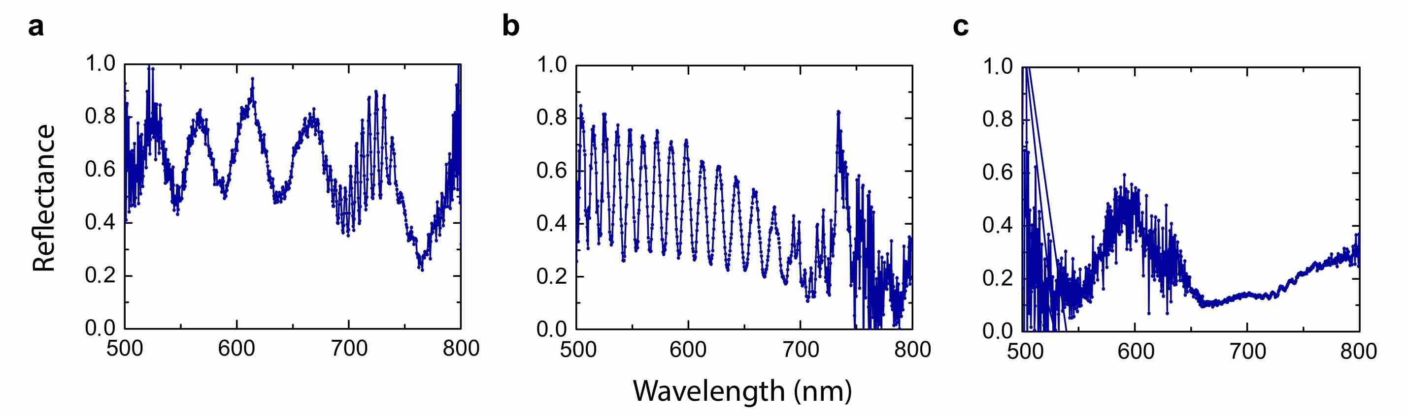
Figure 3a shows the schematics of the experimental setup used to measure the optical response of the 1D PC (described in Methods section). In Fig. 3b and c, we display the effect of the number of periods on the reflectance spectra. Continuous and dashed curves correspond to the experimental and theoretical results obtained when is equal to 1 and 5, and the temperature is kept constant at K, respectively. Even though measured spectra are in agreement with the theoretical predictions, the overall behaviour presents a considerable number of resonant peaks and a small variation in reflectance intensity. Based on the TEM analysis of Fig. 2, we associate these peaks to the possible nonuniformity of the thickness and the additional presence of few YBCO grains grown along the [001] direction. Additionally, a correspondence between the number of interference fringes (or bands) and the number of periods of bilayers in the structure is noticeable. We argue that these fringes are the result of the interference of incident light beams partially reflected and transmitted at the interfaces between layers.
To gain further insight into the optical response of our structure we used the transfer matrix method (see the Methods section) to calculate the reflectance spectra González et al. (2018); Markoš and Soukoulis (2008), and the two fluid model Orlando and Delin (1991), to consider the contribution of the superconductor (YBCO) to the dielectric response of the PC. As we describe below, this model allowed us to theoretically explain the reflectance experimentally found. In order to examine in detail the bands dependence on the number of periods, in Fig. 3e we plot the simulated gap map in the whole range from to 10. The dark areas correspond to the photonic band gaps (PBGs) or high-reflectance ranges, while yellow areas indicate transmission ranges where radiation passes trough the structure. It is noticeable for that the reflectance decreases from 500 nm to approximately 610 nm (see Fig. 3b), which is observed in the gap map of Fig. 3e as the change from dark to yellow region. In the case , two ranges of low reflectance are seen around 510 nm and 620 nm (Fig. 3c), which is completely in agreement with the theory. We have extended our results up to , to show the sensitivity of the PBGs with : the larger , the lower the wavelengths of the photonic bandgaps, and their gap structure experiences a switch for the EM waves propagation from forbidden to allowed frequency ranges at a given wavelength. Interestingly, such structured gaps become narrower as changes from an even to an odd number, which could be exploited as an optical switch.
The two-fluid model is often used to describe the behaviour of a superconductor at nonzero temperature. It consists of two distinct noninteracting fluids of electrons that carry current, where each fluid follows two parallel channels, one superconductor and one normal. Accordingly, when a material is superconducting, some of the electrons will be superconductors and some will still be normal electrons. Thus, there will be a mixture of superelectrons and normal electrons. For these reason, we can model the total conductivity as follows: for , as the sum of the normal conductivity maintained by unpaired electrons, and the superconducting conductivity maintained by superelectrons; and for , by the Drude conductivity for a normal metal. More explicitly, it can be written as Orlando and Delin (1991):
| (1a) | |||||
| (1b) |
where is the EM wave frequency, is the permeability of free space; , , and are respectively the density, the charge, and the mass of the carrriers, denotes the scattering time of electrons. The damping frequency , gives the density of normal state electrons over the total number of electrons, and is the temperature-dependent penetration depth Orlando and Delin (1991):
| (2) |
where is the value of the penetration depth at zero temperature, and the exponent corresponds to 2 and 4 for high and low temperature superconductors, respectively.
The dielectric response of a given material is introduced by means of the electric permittivity. This parameter is in general a complex number, , where the imaginary part accounts for electromagnetic losses in the material and is closely related to the current inside the material through the complex conductivity , such that , where is the dielectric function at high frequencies and the permittivity of free space Bennemann and Ketterson (2008). By replacing equation (1a) into , we arrive at the dielectric function of the superconductor
| (3) |
Finally, substitution of equation (1b) leads to the dielectric function of a metal
| (4) |
To calculate the reflectance spectra, in our numerical simulations layer 1 corresponds to with nm; Wemple et al. (1968). As the operation temperature in the present experiment varies from 20 K to 150 K, the -dielectric constant can be considered constant in this range Kay and Vousden (1949); Merz (1949). Layer 2 corresponds to , with , K (the critical temperature experimentally obtained in this work), nm, the plasma frequency rad/s Lin et al. (2010), the damping frequency rad/s Lin et al. (2010), and the dielectric constant is modelled by equation (3). According to the growth direction of the bilayers (c-axis), we consider the parallel propagation to the c-axis of YBCO, i.e., the magnetic field perpendicular to (TE case). Therefore, the penetration depth is on the a-b plane with a nm Kamal et al. (1994). For temperatures close to the critical temperature , over the range , we adopted the magnetic penetration depth , with Kamal et al. (1994). Simultaneously, we considered the thermal expansion effect on and thicknesses. In certain temperature ranges, the thermal expansion effect adopts the law , where is the thermal expansion coefficient, is the temperature deviation, and and are the thicknesses of each layer under actual and room temperature, respectively Kawashima et al. (1998). We consider the thermal expansion coefficients to be C and C for Keyston et al. (1959) and Wu and Gao (2015) , respectively.
In a previous work González et al. (2018), we have theoretically studied the transmission of the superconductor PC as a function of the wavelength for different temperatures. We found no noticeable changes in the transmission spectra with temperature, but the existence of small shifts in the PBGs were observed. With the aim to compare with experimental results, in Fig. 3d, we plot in six panels, the temperature effect on the measured reflectance spectra. From panels (A), (B), and (C), where the temperature was varied from 80 K, 50K to 30 K for , an almost negligible shift is perceived in the wavelength ranges where the PBGs are present. Similar features were obtained in panels (D), (E) and (F), for with K, 50K and 30 K, respectively. In figure 3d we have indicated with vertical red lines specific wavelengths (, 720, and 760 nm for , and , 625, and 770 nm for ) to get a better visualisation of these findings. In addition, in Fig. 3f, we show the 1D PC reflectance spectrum as a function of wavelength and temperature , from K to 80 K, below the critical temperature of the superconductor. As in the previous case, dark areas correspond to the photonic band gaps (PBGs) or high-reflectance ranges, while yellow areas, indicate high transmission ranges where radiation passes trough the structure. We obtain a negligible shift as the temperature increases. We associate our findings with the slight decreasing suffered by the superconductor dielectric constant as the wavelength increases. If this change were appreciable, the reflectance should suffer a displacement, in agreement with the electromagnetic variational principle Joannopoulos et al. (2011). Thus, our results demonstrate the effectiveness of the implemented 1D PCs as an excellent candidate for the design of an optical transmitter/reflector below and above critical superconductor temperature. The fact that temperature does not significantly affect the operation frequencies of the PBGs becomes an advantage since high reflectances can be achieved in that whole range of temperatures.
Figure 4a and b plot the measured reflectance for 1D PC in the wavelength range from 500 to 700 nm at K and incident angles of and for TE polarization. Two regions of high reflectance were found around 570 nm and 650 nm at and , respectively. For a better understanding of the reflectance behaviour, we have displayed in Fig. 4(c), the spectra as a function of the whole range of incident angles for TE polarization. One important feature found in our results related with the reflection from a finite multilayer is its sensitive response to the angle of incidence of light Joannopoulos et al. (2011), which is observed in the continuous displacement of PBGs to shorter wavelength as the incident angle increases. On the other hand, as the angle of incidence approaches , the reflection coefficient tends to 1, a result in agreement with the fact that a wave that impinges with a right angle moves parallel to the separation surface of the two media, and therefore, its energy is not transmitted through the surface. The results for and (magenta vertical lines) are indicated in the figure, whose bands match perfectly well with measured spectra (Fig. 4 a and b). The gap map also allows to evidence the existence of a third transmission band for wavelengths above 700 nm. These results allow us to conclude that there exist wavelength ranges where the radiation does not pass through the PC under any incident angle, results that can be applied, for example, to tune optical transmitter/reflector fabricated below critical superconductor temperature whose response is sensitive to the angle of incidence of light.
For the sake of completeness, we calculate the optical response of 1D PC when the YBCO is in the non-superconducting state, above . In this case, the dielectric function is described by the Drude model of a metal given by equation (4). The steady-state conductivity () and resistivity () are functions of the plasma frequency and the damping , and they are related as followsOrlando and Delin (1991)
| (5) |
Figure 1(c) presents the YBCO resistivity measured as a function of the temperature. As it is shown, there is an abrupt change in the resistance of the YBCO. For temperatures below there is no resistance, and for temperatures above there is a non-zero resistance that varies linearly with the temperature. Resistivity measurements were performed with and without applied laser field radiation on the 1D PCs. The main idea of this measurement was to confirm that the superconductor () remains in the superconducting state under applied radiation. Even though the superconductor was radiated at frequencies above its superconductor gap ( 8 THz), the 10 mW laser power in the spectral band of 450-750 nm is not enough to destroy the superconducting state.
Accordingly, in equation (5), the damping varies linearly with temperature in accordance with for , which implies that equation (4) is temperature-dependent. The calculated and measured reflectance are shown in Fig. 4d, and the behaviour predicted by the Drude model is in excellent agreement with our experimental results about the reflection of electromagnetic waves at the interface between the ferroelectric and the superconductor in normal state. When the electromagnetic wave impinges on the conductor surface induces a conduction current, which leads to a swift damping of the field inside the conductor. This is why metals have excellent reflecting properties (i.e., reflectance close to unity) and are broadly used in mirrors or optical reflectors. According to the above, a high reflectance would be expected in the PC now composed of the superconductor in the normal state. However, as it is observed in the figures 4d and e, the intensity of the reflectance increases with respect to the previous cases, but it is not total because about 60% and 40% of the light is still transmitted through the structure at certain wavelengths between 500 nm and 700 nm, at K and K, respectively. It is important to point out that reflectivity also depends on the thickness of the layers, and our findings clearly illustrate such thickness dependence Williamson et al. (2016); Shalaev et al. (2019).
In order to analyse the superelectrons contribution on the optical response of the 1D PC, in figure 4f, we report the difference between the reflectance coefficients (R) calculated from the subtraction of the reflectance spectra with and without the superelectron effect according to equations (3) and (4). This result allows us to approximate the magnitude order of the contribution made by the Cooper pairs in the mixed state of the superconductor, below critical temperature, to be of the order , and corroborate their significant contribution to the optical response of the superconductor. From the reflectance spectra at K (), and at K, 50 K and 30 K (), as can be seen in figure 3d, panels D, E, and F, for , we get a decreasing of the reflectance at low temperatures for wavelengths between 500 - 550 nm, and 600 - 650 nm, which implies that the main contribution to the light transmission in the structure is due to the superelectrons. This result highlights the important role played by the superconductor in the optical response of PC. On the other hand, it is worth noting that the Drude model matches perfectly well with the experimental spectrum at 80 K, that is, the temperature around which the states transition occur; however, this model does not adjust the measurements above (e.g., at K). Although the Drude model is presented for temperatures above critical temperature, it is evident that for , there exist additional contributions to the electronic properties affecting the optical response.
Finally, reflectance spectra of heterostructures for , at K are shown in Fig. 5. The reflection spectra for and structures at K clearly shows a constructive interference effect between the incoming light in the YBCO and the reflected light on the YBCO/BTO interface, bearing in mind that the BTO refraction index is larger than that of the YBCO. This is clearly evidenced since the reflected spectra of the structure shows that a maximum (minimum) takes place at each third of the wavelength of the heterostructure. On the other hand, the reflectance spectrum for begins to exhibit the whole reflectance behaviour of the 1D photonic crystal, as reported in González et al. (2018).
III Conclusions
We have succeeded at experimentally realising ferroelectric/superconductor 1D photonic crystals as suitable engineered nanosystems for tuning and controlling electromagnetic wave propagation in a wide region of the visible spectrum. We were able to fabricate 1D photonic crystals of and 5 pairs of BTO/YBCO bilayers by DC and RF sputtering, onto polished (001) substrates, and studied the effects due to temperature and direction of the incident radiation. We have experimentally demonstrated how to tailor the number of PBGs as a function of , and have also been able to quantify and predict, for any , the frequency range sensitivity and optical properties of the PCs with the direction of the incident EM waves—the larger the angle of incidence the shorter the wavelength and the bigger the width of the PBGs. A key result from an operational point of view is that temperature does not significantly affect the frequency range of the transmission bands, which can be advantageous because this enables either a high or low reflectance, in the whole range of studied temperatures (10-300 K). The contribution made by the Cooper pairs in the mixed state of the superconductor to the PC optical response is of the order of : the superelectrons are the most relevant contribution to the light transmission in the structure, at tested wavelengths between 500–550 nm, and 600–650 nm. Finally, and based on the PCs here implemented, several strategies for the development of quantum materials and novel optoelectronic devices, below critical superconductor temperature and different properties of incident light, are proposed.
Methods
Photonic crystal fabrication
The multilayers were grown on a (001) STO substrate by DC/RF sputtering technique at pure oxygen atmosphere and high pressure ( 3.0 mBar), with a substrate temperature of C. Power density of 7 W/cm2 and 12 W/cm2 were used for YBCO and BTO targets, respectively. X-ray diffraction was used to perform structural characterisation using a Co-K=1.79 Å wavelength. In addition to the local interface analysis, transmission electron microscopy (TEM) was employed. Cross-sectional lamella was prepared from the deposited thin films using a dual beam FEI Helios Nanolab 600i. Initially, the surface of the films was coated by a platinum layer on a sputtering in order to avoid charge accumulation during the process. Then, two platinum layers were applied to protect and avoid damages on the thin films. The lamella is extracted and submitted to a thinning process which ends with the use of a low energy beam to minimize the amorphization. Finally, the lamella is placed into a TEM grid. A Hitachi TEM-microscope HF3300C was operated at 300 kV to acquire the high resolution images of the cross-sectional lamella. The sample was tilted until the nearest zone axis of STO was parallel to the electron beam. Then, high resolution images were acquired at the different layers and interfaces. In addition, electron diffraction patterns were obtained to identify the crystallographic orientation of the layers respect to the substrate. The electrical properties and the superconductor transition temperature () were studied using the traditional four-point technique. The resistance as a function of temperature was measured in the 20-300 K range using silver paint and copper wires. Considering that the top layer was always the BTO layer in the multilayer array, it was necessary to analyse the diamagnetism to identify through thermal demagnetization measurements using a PPMS Quantum design from 10 to 300 K.
Wide range laser reflectance measurements
A supercontinuum fiber laser (Fyla STC 1000) and a monochromator (Fyla TW) were employed to irradiate the sample in the 400-800 nm spectral range. The beam path crosses through a telescope arrangement with a magnification factor of 1x to collimate the laser and control the beam divergence. The light is addressed with aluminum mirrors (95% of reflectance) perpendicularly towards the cryostat (Cryostat Advanced Research System) where the sample is placed under a vacuum of bar and a controlled temperature down to 10 K. The reflection angle is controlled with a homemade sample copper holder inside the cryostat, and set to 35∘ and 65∘ for taking different set of measurements. The reflecting path is collected with a collimation lens and coupled to a multimode optical quartz fiber of 400 m diameter. The fiber is connected to a spectrometer (HD 4000, Ocean Optics), which finally displays the spectra in a workstation. The reference spectra for the reflectance calculations were taken at high temperatures for which the reflection of the sample is higher than all the others.
1D photonic crystal transfer matrix calculation
The studied 1D photonic superlattice has a period , and is composed of alternating layers of a dielectric material and a superconductor , whose widths are labeled as and , respectively. The propagation of an in-plane linearly polarized electromagnetic field is of the form , along the z-axis (see Fig. 1a). By using Maxwell’ s equation for linear and isotropic media, it is demonstrated that the amplitude of the electric field satisfies González et al. (2018); Cavalcanti et al. (2007)
| (6) |
where is the vacuum speed of light, and are respectively, the refraction index and the impedance of each layer material. For a photonic crystal composed of alternating layers of two different materials, equation (6) must be solved by assuming both, the electric field and its first derivative continuous across an interface, which means that the two-component function is continuous through the photonic structure. This condition may be conveniently written by means of a transfer matrix as , where
| (7) |
in such a way that may be written as
| (8) |
with
| (9) |
The reflection coefficients are calculated by
| (10) |
considering the corresponding transfer matrix for periods, which can be written as Markoš and Soukoulis (2008)
| (11) |
where , , and are the elements of the transfer matrix for . Here, are the second-order Chebyshev polynomials.
References
- Shalaev et al. (2019) M. I. Shalaev, W. Walasik, A. Tsukernik, Y. Xu, and N. M. Litchinitser, Nature Nanotechnology 14, 31 (2019), URL https://doi.org/10.1038/s41565-018-0297-6.
- Marpaung et al. (2019) D. Marpaung, J. Yao, and J. Capmany, Nature Photonics 13, 80 (2019), URL https://doi.org/10.1038/s41566-018-0310-5.
- Gurioli et al. (2019) M. Gurioli, Z. Wang, A. Rastelli, T. Kuroda, and S. Sanguinetti, Nature Materials 18, 799 (2019), URL https://doi.org/10.1038/s41563-019-0355-y.
- Priolo et al. (2014) F. Priolo, T. Gregorkiewicz, M. Galli, and T. F. Krauss, Nature Nanotechnology 9, 19 (2014), URL https://doi.org/10.1038/nnano.2013.271.
- Paternò et al. (2018) G. M. Paternò, C. Iseppon, A. D’Altri, C. Fasanotti, G. Merati, M. Randi, A. Desii, E. A. A. Pogna, D. Viola, G. Cerullo, et al., Scientific Reports 8, 3517 (2018), URL https://doi.org/10.1038/s41598-018-21824-w.
- Segal et al. (2015) N. Segal, S. Keren-Zur, N. Hendler, and T. Ellenbogen, Nature Photonics 9, 180 (2015), URL https://doi.org/10.1038/nphoton.2015.17.
- Yang et al. (2019) Y. Yang, Z. Gao, H. Xue, L. Zhang, M. He, Z. Yang, R. Singh, Y. Chong, B. Zhang, and H. Chen, Nature 565, 622 (2019), URL https://doi.org/10.1038/s41586-018-0829-0.
- Bell (1880) A. G. Bell, Nature 22, 500 (1880), URL https://doi.org/10.1038/022500a0.
- Andrews et al. (2001) M. R. Andrews, P. P. Mitra, and R. deCarvalho, Nature 409, 316 (2001), URL https://doi.org/10.1038/35053015.
- Senior (2009) J. M. Senior, Optical Fiber Communications: Principles and Practice (Pearson Education, 2009), ISBN 9788131732663, URL https://books.google.com.co/books?id=ok0XX-3MgMoC.
- Joannopoulos et al. (2011) J. Joannopoulos, S. Johnson, J. Winn, and R. Meade, Photonic Crystals: Molding the Flow of Light - Second Edition (Princeton University Press, 2011), ISBN 9781400828241, URL https://books.google.com.co/books?id=QrTNslcjlZEC.
- Wang and John (2004) R. Wang and S. John, Phys. Rev. A 70, 043805 (2004), URL https://link.aps.org/doi/10.1103/PhysRevA.70.043805.
- Pan et al. (2010) J. Pan, S. Sandhu, Y. Huo, N. Stuhrmann, M. L. Povinelli, J. S. Harris, M. M. Fejer, and S. Fan, Phys. Rev. B 81, 041101 (2010), URL https://link.aps.org/doi/10.1103/PhysRevB.81.041101.
- Wang et al. (2019) Z. Wang, S. Yi, A. Chen, M. Zhou, T. S. Luk, A. James, J. Nogan, W. Ross, G. Joe, A. Shahsafi, et al., Nature Communications 10, 1020 (2019), URL https://doi.org/10.1038/s41467-019-08994-5.
- Xue et al. (2016) W. Xue, Y. Yu, L. Ottaviano, Y. Chen, E. Semenova, K. Yvind, and J. Mork, Phys. Rev. Lett. 116, 063901 (2016), URL https://link.aps.org/doi/10.1103/PhysRevLett.116.063901.
- Park et al. (2008) H.-G. Park, C. J. Barrelet, Y. Wu, B. Tian, F. Qian, and C. M. Lieber, Nature Photonics 2, 622 (2008), URL https://doi.org/10.1038/nphoton.2008.180.
- Susa et al. (2014) C. E. Susa, J. H. Reina, and R. Hildner, Physics Letters A 378, 2371 (2014), ISSN 0375-9601, URL http://www.sciencedirect.com/science/article/pii/S0375960114006343.
- Kuramochi et al. (2014) E. Kuramochi, K. Nozaki, A. Shinya, K. Takeda, T. Sato, S. Matsuo, H. Taniyama, H. Sumikura, and M. Notomi, Nature Photonics 8, 474 (2014), URL https://doi.org/10.1038/nphoton.2014.93.
- Vasić and Gajić (2015) B. Vasić and R. c. v. Gajić, Phys. Rev. Applied 4, 024007 (2015), URL https://link.aps.org/doi/10.1103/PhysRevApplied.4.024007.
- Nirmal et al. (2017) A. Nirmal, A. K. K. Kyaw, W. Jianxiong, K. Dev, X. Sun, and H. V. Demir, IEEE Journal of Photovoltaics 7, 545 (2017).
- Madrid-Úsuga et al. (2019) D. Madrid-Úsuga, C. E. Susa, and J. H. Reina, Phys. Chem. Chem. Phys. 21, 12640 (2019), URL http://dx.doi.org/10.1039/C9CP01398A.
- Basov et al. (2017) D. N. Basov, R. D. Averitt, and D. Hsieh, Nature Materials 16, 1077 (2017), URL https://doi.org/10.1038/nmat5017.
- Tokura et al. (2017) Y. Tokura, M. Kawasaki, and N. Nagaosa, Nature Physics 13, 1056 (2017), URL https://doi.org/10.1038/nphys4274.
- Gambetta et al. (2017) J. M. Gambetta, J. M. Chow, and M. Steffen, npj Quantum Information 3, 2 (2017), URL https://doi.org/10.1038/s41534-016-0004-0.
- Melo-Luna et al. (2017) C. A. Melo-Luna, C. E. Susa, A. F. Ducuara, A. Barreiro, and J. H. Reina, Scientific Reports 7, 44730 EP (2017), URL https://doi.org/10.1038/srep44730.
- Houck et al. (2012) A. A. Houck, H. E. Türeci, and J. Koch, Nature Physics 8, 292 (2012), URL https://doi.org/10.1038/nphys2251.
- Lamata (2017) L. Lamata, Scientific Reports 7, 43768 (2017), URL https://doi.org/10.1038/srep43768.
- Hua et al. (2016) M. Hua, M.-J. Tao, and F.-G. Deng, Scientific Reports 6, 22037 (2016), URL https://doi.org/10.1038/srep22037.
- Welp et al. (2013) U. Welp, K. Kadowaki, and R. Kleiner, Nature Photonics 7, 702 (2013), URL https://doi.org/10.1038/nphoton.2013.216.
- Raymond Ooi et al. (2000) C. H. Raymond Ooi, T. C. Au Yeung, C. H. Kam, and T. K. Lim, Phys. Rev. B 61, 5920 (2000), URL https://link.aps.org/doi/10.1103/PhysRevB.61.5920.
- Takeda and Yoshino (2003) H. Takeda and K. Yoshino, Phys. Rev. B 67, 245109 (2003), URL https://link.aps.org/doi/10.1103/PhysRevB.67.245109.
- Berman et al. (2006) O. L. Berman, Y. E. Lozovik, S. L. Eiderman, and R. D. Coalson, Phys. Rev. B 74, 092505 (2006), URL https://link.aps.org/doi/10.1103/PhysRevB.74.092505.
- Martin and Rappe (2016) L. W. Martin and A. M. Rappe, Nature Reviews Materials 2, 16087 (2016), URL https://doi.org/10.1038/natrevmats.2016.87.
- Rault et al. (2014) J. E. Rault, T. O. Menteş, A. Locatelli, and N. Barrett, Scientific Reports 4, 6792 (2014), URL https://doi.org/10.1038/srep06792.
- Boyn et al. (2017) S. Boyn, J. Grollier, G. Lecerf, B. Xu, N. Locatelli, S. Fusil, S. Girod, C. Carrétéro, K. Garcia, S. Xavier, et al., Nature Communications 8, 14736 (2017), URL https://doi.org/10.1038/ncomms14736.
- Wang et al. (2018) H. Wang, Z. R. Liu, H. Y. Yoong, T. R. Paudel, J. X. Xiao, R. Guo, W. N. Lin, P. Yang, J. Wang, G. M. Chow, et al., Nature Communications 9, 3319 (2018), URL https://doi.org/10.1038/s41467-018-05662-y.
- Cheng et al. (2017) H. Cheng, J. Ouyang, Y.-X. Zhang, D. Ascienzo, Y. Li, Y.-Y. Zhao, and Y. Ren, Nature Communications 8, 1999 (2017), URL https://doi.org/10.1038/s41467-017-02040-y.
- Alexander et al. (2018) K. Alexander, J. P. George, J. Verbist, K. Neyts, B. Kuyken, D. Van Thourhout, and J. Beeckman, Nature Communications 9, 3444 (2018), URL https://doi.org/10.1038/s41467-018-05846-6.
- Castera et al. (2015) P. Castera, D. Tulli, A. M. Gutierrez, and P. Sanchis, Opt. Express 23, 15332 (2015), URL http://www.opticsexpress.org/abstract.cfm?URI=oe-23-12-15332.
- Rosa et al. (2017) A. Rosa, D. Tulli, P. Castera, A. M. Gutierrez, A. Griol, M. Baquero, B. Vilquin, F. Eltes, S. Abel, J. Fompeyrine, et al., Opt. Mater. Express 7, 4328 (2017), URL http://www.osapublishing.org/ome/abstract.cfm?URI=ome-7-12-4328.
- Ma and Yang (2017) N. Ma and Y. Yang, Nano Energy 40, 352 (2017), ISSN 2211-2855, URL http://www.sciencedirect.com/science/article/pii/S2211285517305190.
- Xi et al. (2017) Z. Xi, J. Ruan, C. Li, C. Zheng, Z. Wen, J. Dai, A. Li, and D. Wu, Nature Communications 8, 15217 (2017), URL https://doi.org/10.1038/ncomms15217.
- Ruan et al. (2016) J. Ruan, C. Li, Z. Yuan, P. Wang, A. Li, and D. Wu, Applied Physics Letters 109, 252903 (2016), eprint https://doi.org/10.1063/1.4972786, URL https://doi.org/10.1063/1.4972786.
- Porat and Riess (1994) O. Porat and I. Riess, Materials Science and Engineering: B 22, 310 (1994), ISSN 0921-5107, URL http://www.sciencedirect.com/science/article/pii/0921510794902623.
- Chen et al. (2016) Y. Chen, W. Bian, W. Huang, X. Tang, G. Zhao, L. Li, N. Li, W. Huo, J. Jia, and C. You, Scientific Reports 6, 38257 (2016), URL https://doi.org/10.1038/srep38257.
- Chrisey et al. (1988) D. B. Chrisey, W. G. Maisch, G. P. Summers, and A. R. Knudson, IEEE Transactions on Nuclear Science 35, 1456 (1988).
- Wei-Kan et al. (1991) C. Wei-Kan, J. R. Liu, and Z. H. Zhang, Nuclear Instruments and Methods in Physics Research Section B: Beam Interactions with Materials and Atoms 59-60, 1447 (1991), ISSN 0168-583X, URL http://www.sciencedirect.com/science/article/pii/0168583X91958514.
- Quéré (1988) Y. Quéré, Nuclear Instruments and Methods in Physics Research Section B: Beam Interactions with Materials and Atoms 33, 906 (1988), ISSN 0168-583X, URL http://www.sciencedirect.com/science/article/pii/0168583X88907082.
- Poole et al. (2014) C. Poole, R. Prozorov, H. Farach, and R. Creswick, Superconductivity: Third edition (2014).
- Springer et al. (2016) D. Springer, S. K. Nair, M. He, C. L. Lu, S. A. Cheong, T. Wu, C. Panagopoulos, E. E. M. Chia, and J.-X. Zhu, Phys. Rev. B 93, 064510 (2016), URL https://link.aps.org/doi/10.1103/PhysRevB.93.064510.
- Alberca et al. (2015) A. Alberca, M. A. Uribe-Laverde, Y. W. Windsor, M. Ramakrishnan, L. Rettig, I. Marozau, J.-M. Tonnerre, J. Stahn, U. Staub, and C. Bernhard, Phys. Rev. B 92, 174415 (2015), URL https://link.aps.org/doi/10.1103/PhysRevB.92.174415.
- Manthiram et al. (1987) A. Manthiram, J. S. Swinnea, Z. T. Sui, H. Steinfink, and J. B. Goodenough, Journal of the American Chemical Society 109, 6667 (1987), URL https://doi.org/10.1021/ja00256a019.
- Bruynseraede et al. (2007) Y. Bruynseraede, J. Vanacken, B. Wuyts, C. van Haesendonck, J.-P. Locquet, and I. Schuller, Physica Scripta 1989, 100 (2007).
- Pan et al. (2003) V. M. Pan, C. G. Tretiatchenko, V. S. Flis, V. A. Komashko, O. A. Kalenyuk, E. A. Pashitskii, A. N. Ivanyuta, G. A. Melkov, H. W. Zandbergen, and V. L. Svetchnikov, Journal of Superconductivity 16, 889 (2003), ISSN 1572-9605, URL https://doi.org/10.1023/A:1026267321290.
- Zhang et al. (2016) W. Zhang, T. Miller, C. L. Smallwood, Y. Yoshida, H. Eisaki, R. A. Kaindl, D.-H. Lee, and A. Lanzara, Scientific Reports 6, 29100 (2016), URL https://doi.org/10.1038/srep29100.
- Gedik et al. (2004) N. Gedik, P. Blake, R. C. Spitzer, J. Orenstein, R. Liang, D. A. Bonn, and W. N. Hardy, Phys. Rev. B 70, 014504 (2004), URL https://link.aps.org/doi/10.1103/PhysRevB.70.014504.
- Yang et al. (2015) F. Yang, M. Y. Han, and F. G. Chang, Scientific Reports 5, 11504 (2015), URL https://doi.org/10.1038/srep11504.
- Chisholm and Pennycook (1991) M. F. Chisholm and S. J. Pennycook, Nature 351, 47 (1991), URL https://doi.org/10.1038/351047a0.
- González et al. (2018) L. E. González, J. E. Ordoñez, G. Zambrano, and N. Porras-Montenegro, Journal of Superconductivity and Novel Magnetism 31, 2003 (2018), URL https://doi.org/10.1007/s10948-017-4427-4.
- Markoš and Soukoulis (2008) P. Markoš and C. M. Soukoulis, Wave Propagation (Princeton University Press, 2008), ISBN 9780691130033, URL http://www.jstor.org/stable/j.ctt7s2wj.
- Orlando and Delin (1991) T. Orlando and K. Delin, Foundations of Applied Superconductivity, Electrical Engineering Series (Addison-Wesley, 1991), ISBN 9780201183238, URL https://books.google.com.co/books?id=7yRRAAAAMAAJ.
- Bennemann and Ketterson (2008) K. Bennemann and J. Ketterson, Superconductivity: Volume 1: Conventional and Unconventional Superconductors Volume 2: Novel Superconductors, SpringerLink: Springer e-Books (Springer Berlin Heidelberg, 2008), ISBN 9783540732532, URL https://books.google.com.co/books?id=PguAgEQTiQwC.
- Wemple et al. (1968) S. Wemple, M. Didomenico, and I. Camlibel, Journal of Physics and Chemistry of Solids 29, 1797 (1968), ISSN 0022-3697, URL http://www.sciencedirect.com/science/article/pii/0022369768901649.
- Kay and Vousden (1949) H. Kay and P. Vousden, The London, Edinburgh, and Dublin Philosophical Magazine and Journal of Science 40, 1019 (1949), eprint https://doi.org/10.1080/14786444908561371, URL https://doi.org/10.1080/14786444908561371.
- Merz (1949) W. J. Merz, Phys. Rev. 76, 1221 (1949), URL https://link.aps.org/doi/10.1103/PhysRev.76.1221.
- Lin et al. (2010) W.-H. Lin, C.-J. Wu, T.-J. Yang, and S.-J. Chang, Opt. Express 18, 27155 (2010), URL http://www.opticsexpress.org/abstract.cfm?URI=oe-18-26-27155.
- Kamal et al. (1994) S. Kamal, D. A. Bonn, N. Goldenfeld, P. J. Hirschfeld, R. Liang, and W. N. Hardy, Phys. Rev. Lett. 73, 1845 (1994), URL https://link.aps.org/doi/10.1103/PhysRevLett.73.1845.
- Kawashima et al. (1998) J. Kawashima, Y. Yamada, and I. Hirabayashi, Physica C: Superconductivity 306, 114 (1998), ISSN 0921-4534, URL http://www.sciencedirect.com/science/article/pii/S0921453498003505.
- Keyston et al. (1959) J. R. G. Keyston, J. D. Macpherson, and E. W. Guptill, Review of Scientific Instruments 30, 246 (1959), eprint https://doi.org/10.1063/1.1716527, URL https://doi.org/10.1063/1.1716527.
- Wu and Gao (2015) J. Wu and J.-X. Gao, Optik - International Journal for Light and Electron Optics 126 (2015).
- Williamson et al. (2016) I. A. D. Williamson, S. H. Mousavi, and Z. Wang, Scientific Reports 6, 25301 (2016), URL https://doi.org/10.1038/srep25301.
- Cavalcanti et al. (2007) S. B. Cavalcanti, M. de Dios-Leyva, E. Reyes-Gómez, and L. E. Oliveira, Phys. Rev. E 75, 026607 (2007), URL https://link.aps.org/doi/10.1103/PhysRevE.75.026607.
Acknowledgements
This work has been supported by COLCIENCIAS under grant No. 1106-712-49884, the Colombian Science, Technology and Innovation Fund-General Royalties System (Fondo CTeI-Sistema General de Regalías) under contract BPIN 2013000100007, Universidad del Valle CI 71062, and the Center of Excellence for Novel Materials-CENM. L.E.G. is grateful to COLCIENCIAS for financial support (grant No. 811-2018) and Universidad de Ibagué CI 19-505-INT. The authors are grateful to M. A. Hernández-Landaverde of CINVESTAV Queretano-México, for technical assistance and analysis of XRD measurements, and to J. Douin, for facilitating TEM measurements at the Centre d’É laboration de Matériaux et d’Etudes Structurales (CEMES), Toulouse, France.
Author contributions statement
L. E. G. and J. E. O. contributed equally to this work. J.E.O. and E.M. fabricated and structurally characterised the samples, C.A.M-L. conceived and performed the optical measurements together with J.E.O. and E.M., D.R. carried out the TEM characterisation, and L.E.G. performed the analytical and numerical calculations. L.E.G., J.H.R., J.E.O., C.A.M-L., G.Z., N.P-M., M.E.G. and J.C.G., contributed to the analysis and writing of the manuscript, and with discussion, corrections, feedback and comments.