Mechanical deformations of graphene induce a term in the Dirac Hamiltonian which is reminiscent of an electromagnetic vector potential. Strain gradients along particular lattice directions induce local pseudomagnetic fields and substantial energy gaps as indeed observed experimentally. Expanding this analogy, we propose to complement the pseudomagnetic field by a pseudoelectric field, generated by a time dependent oscillating stress applied to a graphene ribbon. The joint Hall-like response to these crossed fields results in a strain-induced charge current along the ribbon. We analyze in detail a particular experimental implementation in the (pseudo) quantum Hall regime with weak intervalley scattering. This allows us to predict an (approximately) quantized Hall current which is unaffected by screening due to diffusion currents.
Quantum Hall response to time-dependent strain gradients in graphene
pacs:
61.48.GhGraphene offers a fertile ground to explore the rich physics of crystalline Dirac materials. A simple tight binding Hamiltonian with a constant hopping amplitude between carbon atoms gives a fair band structure description of many graphene-based systems. Famous examples include single layer graphene with its linearly dispersing (massless) Dirac fermions Wallace (1947); Novoselov et al. (2005), electrically-biased bilayers with a displacement-field-induced band gap McCann and Fal’ko (2006); Castro et al. (2007), or twisted layers with (almost) nondispersing (flat) bands and externally tunable electron correlations Bistritzer and MacDonald (2011); Cao et al. (2018). Graphene is also outstanding in its mechanical stability. The unit cell can stretch by more than 20 without breaking Lee et al. (2008), thus allowing for significant tuning of the hopping amplitude t by applying external stress Amorim et al. (2016); Si et al. (2016); Akinwande et al. (2017). Combining these unique electronic and mechanical resources is highly appealing, and promises novel “straintronic” phenomena as well as practical electromechanical couplings.
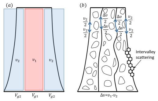
One challenge is to open band gaps by straining the monoatomic hexagonal lattice. The two Dirac points appearing near the and points are protected against perturbations that keep inversion and time reversal symmetries intact, as is the case for uniform (possibly anisotropic) strain. Anisotropic strain replaces the single parameter t by three hopping amplitudes and [see Fig. 1(a)] and shifts the Dirac points in reciprocal space. Interestingly, the difference between the three amplitudes translates into a fictituous vector potential , appearing in the Dirac Hamiltonian Manes (2007), , with and (with the Fermi velocity, the lattice spacing, and ). The strain-induced term , acts within each valley as an external electromagnetic vector potential. However, in order to preserve time reversal symmetry, this “pseudo” vector potential acquires opposite signs in the two valleys. Its magnitude can be expressed in terms of the strain tensor components Manes (2007); Suzuura and Ando (2002); Guinea et al. (2010a),
| (1) |
with .
For carriers in a specific valley, the pseudo vector potential implies electric and magnetic fields. The former, , is induced by time dependent strains, while the latter, , requires specific strain gradients Sasaki et al. (2005); Guinea et al. (2010a, b); Vozmediano et al. (2010). Experimentally, scanning tunneling spectroscopy Levy et al. (2010); Jiang et al. (2017) on triangularly strained graphene found tunneling resonances with a Landau-level-like spacing that indicated remarkably large pseudomagnetic fields exceeding . Recent ARPES spectra Nigge et al. (2019) on multiple triangular islands of graphene further confirm the pseudo-Landau level (PLL) picture of flat bands separated by more than . The large energy gaps exceed room temperature and promise fascinating correlation physics as well as practical technological opportunities. Detecting the pseudoelectric fields on the other hand remains challenging von Oppen et al. (2009). Unavoidable lattice deformations also induce a scalar potential due to compression or dilation of the unit cell. While the scalar field acts equally on both valleys, the pseudoelectric field switches sign between the valleys, and generates valley rather than charge currents.
Here we propose a way to observe the pseudoelectric field through charge currents by combining time-dependent and spatially varying strains which introduce both pseudo- and pseudo fields. The concept is similar to the Hall effect where a transverse drift velocity is generated in the presence of non-parallel fields. While the direction of each individual field is opposite for electrons from the two valleys, the Hall-like drift velocity involves both fields and points in the same direction for both valleys.
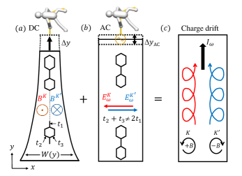
We demonstrate this general concept in a particular and experimentally feasible geometry of a graphene ribbon under uniaxial stress Zhu et al. (2015). As sketched in Fig. 1(a), we set the stress and the lattice armchair direction along the ribbon, while the width of the ribbon is narrowing toward its top end. The stress leads to for this orientation, while the change in induces strain gradients and thus a pseudo field. To generate a pseudo field in the transverse direction we add a small AC stress component to the fixed DC strain, see Fig. 1(b). Together, the two intrinsic fields generate a drift motion along the ribbon for electrons from both valleys and thus an oscillating charge current , see Fig. 1(c). Classically, the current is given by , where is the density measured from the Dirac point. Defining the filling factor , this non quantized current translates into , where is an AC pseudo-voltage difference induced by the intrinsic pseudo- field. While in principle detectable, we show that is usually minute for AC strain frequencies smaller than GHz due to fast and efficient screening by diffusing electrons. Our main prediction is that a sizable charge response can be observed when the pseudo- field is sufficiently strong to cause the formation of PLLs. In this regime, the presence of energy gaps efficiently suppresses screening and a Hall-like is expected for a wide range of frequencies, deformations, and doping levels, provided that intervalley scattering is weak. We suggest a particular device realization where these requirements can be achieved, and compare the conventional quantum Hall (QH) response for static magnetic fields, both externally applied and strain induced, to the dynamic pseudo QH response which is the main prediction of this paper.
System— We envision a micrometer scale geometry as shown in Fig. 2(a). The ribbon is clamped at the top and bottom ends and pulled by metallic beams, which are also used to measure the charge transport response. We compute the mechanical response by COMSOL finite element simulations, adjusting the external stretch to nm to induce a maximum local strain of 20. Beyond this stretch the narrow (top) part of the ribbon will rupture. Naturally, variations in the ribbon’s width translate into gradients in along the direction [see Fig. 2(c)], and hence to a finite . More specifically, the shape function is selected such as to optimize a constant gradient in and hence a uniform pseudo- field over a large section of the ribbon Zhu et al. (2015); app . The color map in Fig 2(b) shows and the calculated strain tensor components. For the specific dimensions presented we obtain a nearly constant T over m at the center of the ribbon, see the black line in Fig. 2(c).
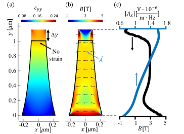
The local pseudo- field is generated by a small AC stress applied in the same direction. We envision a mechanical piezoelectric manipulator that can modulate the strain at a frequency of, say, =10MHz, and assume a small oscillation amplitude such that the device elongates by where nm (leaving approximately unchanged). The orientation of and its magnitude (scaled by a factor ) are determined by and presented at several points in the ribbon by the arrows (size and orientation) in Fig. 2(b). The magnitude of along the line is plotted in Fig. 2(c). As shown, the arrows are pointing primarily in the direction indicating an AC pseudo-voltage difference between the right and left sides of the ribbon. Upon integration, , we find a value mV.
Using a simple elastic theory one can also obtain analytic approximations of the two pseudofields app , , and . In the latter, the three factors display the dependence on the ribbon’s stretching deformation , narrowing parameter , and overall dimension . In the last dimensionful factor, Zhu et al. (2015) is the Poisson ratio and m. The field depends directly on and thus increases along the narrowing ribbon as , see Fig. 2(c). Finally, we note that the frequencies considered are low compared to all relevant electronic and elastic modes and hence we will treat the pseudo- field as quasi-static.
Both the simulated and analytic results presented above show relatively large and uniform intrinsic fields over a micrometer size sample. Compared to the nano-scale systems considered to date, this leads to several advantages: finite size effects are minute, the magnetic length is significantly smaller than the system size, and the cyclotron radius can be tuned below the system’s dimensions by an external gate. Thus, the proposed system allows us to consider the QH regime with (with the cyclotron frequency ) generated by pure strain.
Quantum Hall regime: static case— Before considering AC strain and the associated pseudo- field, we discuss transport in the integer QH regime, contrasting the case of an external magnetic field against an intrinsic pseudo- field, as probed by a two-probe measurement.
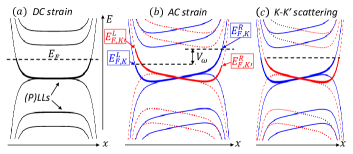
Here, we focus on the clean case, and argue that disorder just renders the QH physics more robust Halperin (1982); Imry (2002); Prange and Girvin (1990). To visualize the LLs and PLLs for these two cases, Fig. 3(a), consider a Corbino disk geometry (i.e., our geometry with a periodic and translation invariant direction). We can then label states by their momenta , which are related to . For an external magnetic field . In contrast, for a pseudo- field and are related differently for the two valleys, . The current follows by summing over the contributions of all occupied states, . Once the Fermi level lies in the bulk gap between LLs (or PLLs), each (P)LL contributes a quantized current Halperin (1982); Imry (2002)
| (2) |
in a two-terminal setup. Here, is the external voltage applied between the two terminals.
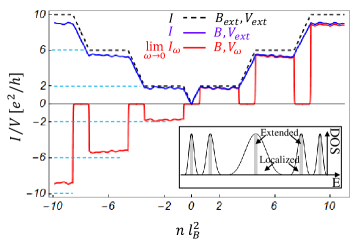
For an external magnetic field, the edge modes are chiral. The voltage at the source terminal feeds into one of the two edges, say the right edge, elevating its chemical potential for both valleys with respect to the opposite edge Datta (1997), i.e., . Summing over spin and valley, this leads to a sequence of quantized plateaus in the two-terminal conductance , where , see the black dashed curve in Fig. 4. The current is quantized and protected by the large distance between the counterpropagating chiral edge modes.
The pseudo- field, on the other hand, spatially superimposes counterpropagating edge states from the two valleys. Thus the system is no longer protected against backscattering, and we expect a nonquantized two-terminal conductance Low and Guinea (2010). The external voltage now imposes opposite interedge chemical potential differences in the two valleys, . Nevertheless, approximate quantization is expected if the disorder potential is smooth on the atomic scale and intervalley scattering is suppressed, see the blue curve in Fig. 4 Morpurgo and Guinea (2006); rem . This is possible, for example, by effectively introducing smooth edges as described in Appendix B.
A few comments on our assumptions for the formation of PLLs are in order. To obtain translation invariance along the direction we use the gauge rather than . Note that our synthetic gauge theory is actually not gauge invariant in the presence of generic intervalley coupling, since the two valleys transform differently. Gauge invariance applies only to each valley separately. Exploiting gauge invariance assumes that valley is a good quantum number. This requires negligible intervalley scattering both in the bulk and on the edges, as discussed above. Additionally, we comment that while Fig. 3(a) shows flat bands, PLLs are not necessarily flat Lantagne-Hurtubise et al. (2019).
Quantum Hall regime: dynamic case— Now, rather than considering a voltage difference between infinite reservoirs, we dynamically apply an intrinsic pseudo- field, generating a potential difference between the edges. This leads to oppositely tilting PLLs in the two valleys as shown in Fig. 3(b). As long as a bulk gap remains open between the tilted PLLs, which requires , the current depends solely on the chemical potential difference between the edges. We have , so that Eq. (2) predicts approximately quantized plateaus for weak intervalley scattering (cf. the two-terminal case with pseudo- field). Thus, in the gap-dominated regime our AC pseudo Hall effect is quantized with , even at low frequencies. This AC charge current in response to the pseudo- field is our main result. The resulting plateaus are schematically displayed in Fig. 4 by the red curve. In the presence of intervalley scattering we expect the edges to equilibrate, see Fig. 3(c). From the above estimate of a 0.1mV pseudo-voltage, we obtain for filling factor .
Notice that while the two-terminal conductance is necessarily positive, the pseudo- response in fact changes sign across the Dirac point, see the red curve in Fig. 4. This is a consequence of the sign change in the group velocity of the edge states upon going from electron to hole doping.
Another crucial difference between the external voltage between infinite reservoirs and the intrinsically generated transverse voltage is that the latter will be screened by electronic diffusion across the ribbon on time scales much faster than the AC frequency. This is reflected in the red curve in Fig. 4 where the current response drops to zero at QH transitions due to screening in these delocalized situations. The same effect of the pseudo- field will occur for any gapless system, in particular for small pseudo- fields with . We now discuss this screening at finite frequency within a semiclassical treatment.
Gapless (screened) regime— The interplay of a dissipative conductivity with the edges of the sample and the resulting valley polarization can be described via the transport equation
| (3) |
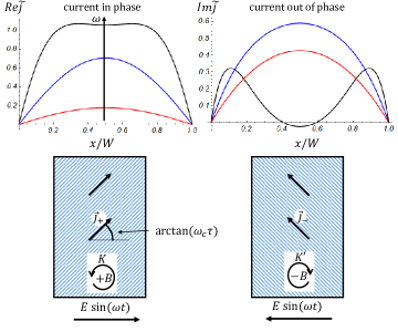
for the current densities and charge densities of the two valleys. The conductivity is related to the diffusion coefficient via the Einstein relation. The last term in Eq. (3) is a Hall term. The edges of the sample imply the boundary condition . We provide a closed form solution of this equation (combined with the continuity equation) in Appendix C. It can be written in terms of two dimensionless parameters. In addition to , the typical time scale for traversing the sample, , introduces a second dimensionless parameter , which controls the reduction of the current due to screening by valley-dependent diffusion currents.
For screening is not effective. In this regime the current takes the Drude form for an infinite system, and is in phase with the pseudo- field. At low frequencies, we find app , which is out of phase with the pseudo- field. In the system in Fig. 1, with MHz, we estimate , leading to a strong reduction of the current at the QH transitions. For we obtain . In principle, however, the effect can be observed even in a gapless regime, provided the frequency is sufficiently high, .
Conclusion— We presented a novel mechanism to generate charge currents from space and time dependent strain fields in graphene, by combining crossed pseudo- and pseudo- fields. A related charge current response was found Vaezi et al. (2013) by gapping out graphene by a mass corresponding to a sublattice potential (e.g. due to h-BN encapsulation), which plays the role of the time reversal invariant and tunable PLL gap in our case. The charge current response should be contrasted with previous theoretical works on transport in strained graphene, predicting valley-polarized currents in the presence of external magnetic fields Low and Guinea (2010); Settnes et al. (2016a); Ma et al. (2016); Milovanović and Peeters (2016); Settnes et al. (2017); Muñoz and Soto-Garrido (2017), including valley filters or switches Zhai et al. (2010); Fujita et al. (2010); Wu et al. (2011); Settnes et al. (2016b); Stegmann and Szpak (2018); Prabhakar et al. (2019); Wu et al. (2017), by combination with polarized light Golub et al. (2011), parametric pumping Jiang et al. (2013); Wang et al. (2014), or even in equilibrium in a zigzag graphene ribbon Lantagne-Hurtubise et al. (2019).
The relatively simple and analytic gauge field treatment of long-wavelength strain in graphene allowed us to analyze inversion symmetry breaking on macroscopic scales, design a tunable static strain-induced bulk gap, and use these to induce a dynamic charge current. We expect this general concept to extend to a wider set of systems and materials, including (3D) Weyl semimetals, which show similar synthetic gauge field effects Pikulin et al. (2016); Grushin et al. (2016); Gorbar et al. (2017); Arjona and Vozmediano (2018). The proposed effect also allows for measuring the edge contribution to intervalley scattering, to which it is highly sensitive even in the static case.
Acknowledgements: We thank Roman Mints for useful discussions. This research was supported by the Binational Science Foundation Grant No. 2016255 (ES), CRC 183 of the Deutsche Forschungsgemeinschaft (FvO), and the Israel Science Foundation Grant No. 1652/18 (MBS).
References
- Wallace (1947) P. R. Wallace, Phys. Rev. 71, 622 (1947).
- Novoselov et al. (2005) K. S. Novoselov, A. K. Geim, S. Morozov, D. Jiang, M. Katsnelson, I. Grigorieva, S. Dubonos, and A. A. Firsov, Nature 438, 197 (2005).
- McCann and Fal’ko (2006) E. McCann and V. I. Fal’ko, Phys. Rev. Lett. 96, 086805 (2006).
- Castro et al. (2007) E. V. Castro, K. Novoselov, S. Morozov, N. Peres, J. L. Dos Santos, J. Nilsson, F. Guinea, A. Geim, and A. C. Neto, Phys. Rev. Lett. 99, 216802 (2007).
- Bistritzer and MacDonald (2011) R. Bistritzer and A. H. MacDonald, Proc. Nat. Acad Sciences 108, 12233 (2011).
- Cao et al. (2018) Y. Cao, V. Fatemi, S. Fang, K. Watanabe, T. Taniguchi, E. Kaxiras, and P. Jarillo-Herrero, Nature 556, 43 (2018).
- Lee et al. (2008) C. Lee, X. Wei, J. W. Kysar, and J. Hone, Science 321, 385 (2008).
- Amorim et al. (2016) B. Amorim, A. Cortijo, F. De Juan, A. Grushin, F. Guinea, A. Gutiérrez-Rubio, H. Ochoa, V. Parente, R. Roldán, P. San-Jose, et al., Phys. Rep. 617, 1 (2016).
- Si et al. (2016) C. Si, Z. Sun, and F. Liu, Nanoscale 8, 3207 (2016).
- Akinwande et al. (2017) D. Akinwande, C. J. Brennan, J. S. Bunch, P. Egberts, J. R. Felts, H. Gao, R. Huang, J.-S. Kim, T. Li, Y. Li, et al., Ext. Mech. Lett. 13, 42 (2017).
- Manes (2007) J. L. Manes, Phys. Rev. B 76, 045430 (2007).
- Suzuura and Ando (2002) H. Suzuura and T. Ando, Phys. Rev. B 65, 235412 (2002).
- Guinea et al. (2010a) F. Guinea, M. Katsnelson, and A. Geim, Nat. Phys. 6, 30 (2010a).
- Zhu et al. (2015) S. Zhu, J. A. Stroscio, and T. Li, Phys. Rev. Lett. 115, 245501 (2015).
- Sasaki et al. (2005) K.-I. Sasaki, Y. Kawazoe, and R. Saito, Prog. Theo. Phys. 113, 463 (2005).
- Guinea et al. (2010b) F. Guinea, A. Geim, M. Katsnelson, and K. Novoselov, Phys. Rev. B 81, 035408 (2010b).
- Vozmediano et al. (2010) M. A. Vozmediano, M. Katsnelson, and F. Guinea, Phys. Rep. 496, 109 (2010).
- Levy et al. (2010) N. Levy, S. Burke, K. Meaker, M. Panlasigui, A. Zettl, F. Guinea, A. C. Neto, and M. Crommie, Science 329, 544 (2010).
- Jiang et al. (2017) Y. Jiang, J. Mao, J. Duan, X. Lai, K. Watanabe, T. Taniguchi, and E. Y. Andrei, Nano Lett. 17, 2839 (2017).
- Nigge et al. (2019) P. Nigge, A. Qu, É. Lantagne-Hurtubise, E. Mårsell, S. Link, G. Tom, M. Zonno, M. Michiardi, M. Schneider, S. Zhdanovich, et al., arXiv preprint arXiv:1902.00514 (2019).
- von Oppen et al. (2009) F. von Oppen, F. Guinea, and E. Mariani, Phys. Rev. B 80, 075420 (2009).
- (22) See supplemental material.
- Halperin (1982) B. I. Halperin, Phy. Rev. B 25, 2185 (1982).
- Imry (2002) Y. Imry, Introduction to mesoscopic physics (Oxford University Press, 2002).
- Prange and Girvin (1990) R. Prange and S. Girvin, Springer New York (1990).
- Datta (1997) S. Datta, Electronic transport in mesoscopic systems (Cambridge University Press, 1997).
- Low and Guinea (2010) T. Low and F. Guinea, Nano lett. 10, 3551 (2010).
- Morpurgo and Guinea (2006) A. Morpurgo and F. Guinea, Phys. Rev. Lett. 97, 196804 (2006).
- (29) One may imagine adding smoothening backgates parallel to the edges of the narrowing device in order to push the electrons away from the disordered edge of the graphene ribbon, see Appendix B.
- (30) One can also combine the dynamical pseudo AC voltage with an external magnetic field . This generates an AC valley current instead of a charge current, which would not be sensitive to intervalley scattering.
- Lantagne-Hurtubise et al. (2019) É. Lantagne-Hurtubise, X.-X. Zhang, and M. Franz, arXiv preprint arXiv:1909.01442 (2019).
- Settnes et al. (2016a) M. Settnes, N. Leconte, J. E. Barrios-Vargas, A.-P. Jauho, and S. Roche, 2D Materials 3, 034005 (2016a).
- Ma et al. (2016) N. Ma, S. Zhang, and D. Liu, Phys. Lett. A 380, 1884 (2016).
- Milovanović and Peeters (2016) S. Milovanović and F. Peeters, J. Phys.: Cond. Matt. 29, 075601 (2016).
- Settnes et al. (2017) M. Settnes, J. H. Garcia, and S. Roche, 2D Materials 4, 031006 (2017).
- Muñoz and Soto-Garrido (2017) E. Muñoz and R. Soto-Garrido, J. Phys.: Cond. Matt. 29, 445302 (2017).
- Zhai et al. (2010) F. Zhai, X. Zhao, K. Chang, and H. Xu, Phys. Rev. B 82, 115442 (2010).
- Fujita et al. (2010) T. Fujita, M. Jalil, and S. Tan, Appl. Phys. Lett. 97, 043508 (2010).
- Wu et al. (2011) Z. Wu, F. Zhai, F. Peeters, H. Xu, and K. Chang, Phys. Rev. Lett. 106, 176802 (2011).
- Settnes et al. (2016b) M. Settnes, S. R. Power, M. Brandbyge, and A.-P. Jauho, Phys. Rev. Lett. 117, 276801 (2016b).
- Stegmann and Szpak (2018) T. Stegmann and N. Szpak, 2D Materials 6, 015024 (2018).
- Prabhakar et al. (2019) S. Prabhakar, R. Nepal, R. Melnik, and A. A. Kovalev, Phys. Rev. B 99, 094111 (2019).
- Wu et al. (2017) Y. Wu, D. Zhai, C. Pan, B. Cheng, T. Taniguchi, K. Watanabe, N. Sandler, and M. Bockrath, Nano lett. 18, 64 (2017).
- Golub et al. (2011) L. Golub, S. Tarasenko, M. Entin, and L. Magarill, Phys. Rev. B 84, 195408 (2011).
- Jiang et al. (2013) Y. Jiang, T. Low, K. Chang, M. I. Katsnelson, and F. Guinea, Phys. Rev. Lett. 110, 046601 (2013).
- Wang et al. (2014) J. Wang, K. Chan, and Z. Lin, Appl. Phys. Lett. 104, 013105 (2014).
- Vaezi et al. (2013) A. Vaezi, N. Abedpour, R. Asgari, A. Cortijo, and M. A. Vozmediano, Phys. Rev. B 88, 125406 (2013).
- Pikulin et al. (2016) D. Pikulin, A. Chen, and M. Franz, Phys. Rev. X 6, 041021 (2016).
- Grushin et al. (2016) A. G. Grushin, J. W. Venderbos, A. Vishwanath, and R. Ilan, Phys. Rev. X 6, 041046 (2016).
- Gorbar et al. (2017) E. Gorbar, V. Miransky, I. Shovkovy, and P. Sukhachov, Phys. Rev. B 96, 125123 (2017).
- Arjona and Vozmediano (2018) V. Arjona and M. A. Vozmediano, Phys. Rev. B 97, 201404 (2018).
- Sarma et al. (2011) S. D. Sarma, S. Adam, E. Hwang, and E. Rossi, Rev. Mod. Phys. 83, 407 (2011).
Appendix A Appendix A: Programmable gauge fields
In this appendix we briefly review the relation between strain fields and synthetic gauge fields in the geometry of Zhu et. al. Zhu et al. (2015). For completeness we review their main ideas and obtain some further useful formulas specifically for the pseudoelectric field.
Consider applying a force along the direction in Fig. 1. It leads to a stretch by . Force balance along any cut at constant implies where is the stress along , is the “width” of graphene, and is the Young modulus. Using this simple relation one obtains a -dependent strain controlled by the width function ,
| (4) |
Thus, a narrowing width yields a strain gradient
| (5) |
In order to obtain a constant gradient one needs to choose a specific width function. The specific shape function is
| (6) |
where .
Next we would like to obtain all the strain tensor components in order to calculate the pseudo vector potential from Eq. (1). We use the constitutive relations , , and , as well as stress equilibrium . Here is the Poisson ratio, and the shear modulus. Assuming uniaxial stretch we have
| (8) |
Combining these relations one obtains Zhu et al. (2015) and . Under the condition of we have
| (9) |
Thus, this simple elasticity theory allows us to determine the synthetic gauge fields in the device using Eq. (1),
| (10) |
where .
Consider an adiabatically slow time-dependent Force of the form . Using Eq. (1) and the above relations we have
| (11) |
Relating the force to the stretch using Eq. (7), and here ignoring , gives
| (12) |
The first, second, and third factors show the relation between the pseudomagnetic field and the relative stretch, the narrowing percentage, and the overall dimensions of the ribbon. The last dimensionfull factor can be estimated for graphene using m T. For a relative stretch of , , and m, as in Fig. 2, as well as and , this estimate gives Tesla, which is close to our COMSOL simulation.
Similarly, the pseudoelectric field along reads
| (13) |
Note the dependence of the pseudoelectric field as given by from Eq. (6), consistent with our COMSOL simulation in Fig. 2(b),(c).
Appendix B Appendix B: Suppressing intervalley scattering using smooth edges
The pseudo QH effect described in this paper strongly relies on the absence of intervalley scattering. Intraedge intervalley relaxation will suppress the current by a factor where is the length of the edge and is the intervalley scattering length.
In this appendix we argue that this assumption can be satisfied in the modified device in Fig. 5. The idea is that any sort of edge physics on the atomic scale, which typically contain an irregular combination of zigzag and armchair edges, produces intervalley scattering. However one can push the effective edges into the interior of the device, where their scattering becomes dominated by the disorder potential stabilizing the QH effect Prange and Girvin (1990); Imry (2002) whose characteristic length scale is typically assumed to significantly exceed the atomic distance. As a result, the trajectories in the interior of the sample will have an approximately conserved valley quantum number.
Consider adding three gates along the device as shown in Fig. 5(a), allowing independent control of the density in the three regions. We envision these regions to stabilize separate gapped QH states, with the filling factor in the central region being (), controlled by , and in the exterior regions which is assumed to be fixed and controlled by . In the bulk, the QH states consist of localized states, and the different QH states are separated by extended states, as shown in Fig. 5(b) where the typical disorder length exceeds the atomic scale. While the external edge mode trajectories between the region and vacuum are sensitive both to bulk disorder and to atomically sharp irregularities of the physical edge of the graphene sample, the interface edge modes between the and regions are determined solely by the smooth disorder potential.
As a result of the smoothness of the disorder potential, the semiclassical trajectories corresponding to a superimposed fast cyclotron motion on top of a slow drift velocity around the disorder potential, , have a well defined valley character. On the other hand, the edge modes near the edges of the sample are strongly affected by atomically sharp edge scattering and thus undergo intervalley scattering. These two types of 1D modes are spatially separated by the gapped QH region of localized states.
These filling factors dictate the number of edge modes at each interface. For a real magnetic field the number of chiral edge modes is given by the filling factor , or by the difference of filling factors at an interface between two different QH states. But for a pseudomagnetic field these modes are equally split at each edge into the two chiralities, i.e., there are modes moving in each direction. As denoted in Fig. 5(b) the number of edge modes of each chirality is at the exterior edge and at the interior interface between and filling factors. Let us assume for simplicity.
Without intervalley scattering anywhere, the total two-terminal conductance as determined by the number of modes is dictated by the largest filling factor
| (14) |
In the presence of strong intervalley scattering we assume that the external edge modes of the region are gapped out and do not contribute. Then the two-terminal conductance becomes
| (15) |
As a function of the gate voltage controlling the conductance will exhibit nearly quantized plateaus. The AC pseudo Hall effect will follow a similar behavior.
This analysis also implies that one can use such a device to probe the importance of intervalley scattering at the outer edge and test the length scale .
Appendix C Appendix C: AC pseudo Hall current in the diffusive regime
As the density is tuned through the extended PLL states, bulk transport takes place. This means that the pseudoelectric field leads to a finite valley current perpendicular to the edges of the sample. Since the electric field is opposite for the two valleys, this leads to a valley polarization near the edges, which eventually in the DC limit leads to a diffusive current effectively screening the external pseudo- field and suppressing . For finite frequency, this opposing diffusive current does not fully develop. In this appendix we present an approximate semiclassical analysis of the current at finite frequency.
We consider a transport equation for the current densities of the two valleys , which includes a dissipative conductance , a diffusion current, and a Hall effect, as well as the continuity equation,
| (16) | |||||
| (17) |
Here is the diffusion constant. The currents and the densities are related by the continuity Eq. (17), and also satisfy boundary conditions . Again here we ignore intervalley scattering and hence obtain uncoupled equations for the two valleys.
We solve these equations under simplifying assumptions of (i) no dependence of neither the width nor the fields , and (ii) the AC electric field points along the direction only. Then the component of Eq. (16) gives , with , and the component of Eq. (16) yields the differential equation
| (18) |
with boundary condition . The electric field is the real part of and the current contains both in and out of phase components. From the diffusion time across the width of the sample
| (19) |
we form a dimensionless parameter (which takes very low values in our system as estimated below). One recasts the differential equation in terms of dimensionless coefficients, a dimensionless variable , and a source term,
| (20) |
with boundary conditions . It is solved by
| (21) |
where . Having solved for (valley ), we can obtain by replacing and . Flow lines and the current profile as function of are plotted in Fig. 6.
At high frequency screening does not have time to develop. With we have , except right on the edge. This current is in phase with the electric field.
At low frequency we expect a strong suppression of the current due to screening. Expanding the solution for small , corresponding to low frequency, we obtain
| (22) |
which is out of phase with respect to the electric field. We see the suppression factor due to the scrreening effect, which becomes efficient when . Integrating over the width of the sample yields
| (23) |
We now estimate the diffusion time for a width m. Doe the diffusion coefficient we use Einstein’s relation with a typical experimental value for the longitudinal conductivity in graphene at QH transitions Novoselov et al. (2005); Sarma et al. (2011). The density of states depends on disorder as depicted in the inset of Fig. 4. Here we estimate very crudely by assuming a density of states of a clean LL, , spread due to disorder over an energy approximately given by the LL spacing . This estimate is equivalent as an order of magnitude to the Dirac density of states with determined from the electronic density of a full LL, . For T this gives and we obtain giving a time of . For a typical piezoelectric-mechanical frequency we have .
While here we considered piezoelectric modulators, which sets an upper limit for possible frequencies, the effect can in principle be observed at higher frequencies.