Quenching of an antiferromagnet into high resistivity states using electrical or ultrashort optical pulses
Ultra-fast dynamics, insensitivity to external magnetic fields, or absence of magnetic stray fields are examples of properties that make antiferromagnets of potential use in the development of spintronic devices. Similar to their ferromagnetic counterparts, antiferromagnets can store information in the orientations of the collective magnetic order vector. However, also in analogy to ferromagnets, the readout magnetoresistivity signals in simple antiferromagnetic films have been weak and the extension of the electrical reorientation mechanism to optics has not been achieved. Here we report reversible and reproducible quenching of an antiferromagnetic CuMnAs film by either electrical or ultrashort optical pulses into nano-fragmented domain states. The resulting resistivity changes approach 20% at room temperature, which is comparable to the giant magnetoresistance ratios in ferromagnetic multilayers. We also obtain a signal readout by optical reflectivity. The analog time-dependent switching and relaxation characteristics of our devices can mimic functionality of spiking neural network components.
Ferromagnets and antiferromagnets are two fundamental classes of materials with magnetic order. Although antiferromagnets are more readily available than ferromagnets, their magnetic order cannot be easily harnessed Neel1971 . Current-induced spin-orbit fields in ferromagnets with broken inversion symmetry can be used to manipulate the magnetic order vector of a ferromagnet, an effect necessary for the operation of ferromagnetic memories. The reorientation of the magnetic order vector – or switching – has recently been extended to antiferromagnets such as CuMnAs and Mn2Au Shick2010 ; Park2011 ; Chen2014 ; Nakatsuji2015 ; Zelezny2014 ; Wadley2016 , where the local symmetry-breaking of the lattice gives rise to a staggered spin-orbit field Zelezny2018 ; Wadley2016 ; Zelezny2014 ; Bodnar2018 , prompting further research into the symmetry and topology landscape of antiferromagnets Jungwirth2016 ; Baltz2018 ; Jungwirth2018 ; Zelezny2018 ; Nemec2018 ; Smejkal2017b ; Gomonay2018 . In these first antiferromagnetic memories, the readout was based on the anisotropic magnetoresistance (AMR) and the retention originated from the switching between ground states with different directions of the collective Néel vector, similar to the operation of the first generation of ferromagnetic random access memories (MRAMs) Daughton1992 .
The polarity of current pulses with pulse lengths in the s–ms range and threshold currents around Acm-2 was used to demonstrate the reorientation (switching) of the Néel vector in CuMnAs devices Wadley2018 . The observations, obtain by X-ray magnetic linear dichroism photoemission electron microscopy (XMLD-PEEM), showed reproducible, reversible, and stable switching of large, micron-scale antiferromagnetic domains and the measurements were consistent with the expected symmetry of the staggered current-induced field. However, only weak AMR readout signals of % were obtained by switching the large domains in the CuMnAs film Wadley2018 . The small AMR amplitude in single-layer CuMnAs films was independently confirmed in a recent study where the Néel vector reorientation was induced by a strong external magnetic field Wang2020 . On the other hand, multilayers with giant-magnetoresistance, which made ferromagnetic MRAMs a commercially viable technology Chappert2007 , have not been realized in antiferromagnets.
Furthermore, after a decade of research, optical control of magnetism using ultra-short single femtosecond-laser pulses has been demonstrated only for ferrimagnets Kimel2019 ; the reorientation of the ferrimagnetic order vector is based on unequal, light-induced demagnetization dynamics of the different spin-sublattices and this mechanism is not compatible with antiferromagnets. All-optical switching was recently observed in ferromagnets, but requires a complex process involving demagnetization and domain-nucleation and expansion driven by multiple laser pulses Kimel2019 .
In this Article, we report deterministic and reversible changes in the resistivity of a film of antiferromagnetic CuMnAs by using electrical pulses with a current density over Acm-2 or by ultra-short optical pulses. By applying the writing pulses, the antiferromagnet is brought to the vicinity of the magnetic transition point and then quenched into a nano-fragmented domain state with high resistivity. We term this effect quench switching of an antiferromagnet. The corresponding resistivity changes exceed the previously reported AMR signals related to the reorientation switching of the magnetic order vector by up to three orders of magnitude. The quench switching can by also probed optically by reflectivity measurements. The nano-fragmented antiferromagnetic domain state under electrical pulsing conditions has been imaged by diamond NV-center magnetometry Wornle2019 , and we confirm the findings via synchrotron-based XMLD-PEEM measurements. Our observations suggest that the time dependence of the resistivity after the quench switching follows the Kohlrausch stretched-exponential relaxation form.
Electrical switching detected by resistivity or reflectivity
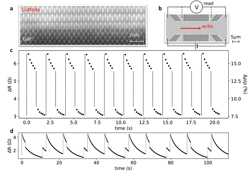
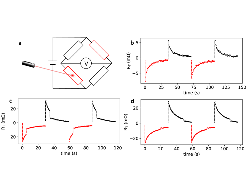
Fig. 1 shows results of the quench switching by unipolar electrical current pulses in a bar resistor at room temperature. Our microdevices (Fig. 1b) were lithographically patterned from a 50 nm thick epilayer of tetragonal CuMnAs of 20 sheet resistance grown by molecular beam epitaxy on an insulating lattice-matched GaP substrate (Fig. 1a) Wadley2013 ; Krizek2020 . In the measurements plotted in Fig. 1c, we use the simplest two-point resistor geometry for delivering the writing pulses and for detecting the readout signals. We start by applying an electrical writing pulse of 100 s and measure for 1 s the resulting change in the ohmic resistance of the device. The pulse induces an increase in the resistance. We then repeat the measurement using a writing pulse of reduced amplitude (by 8%) and observe that the resistance drops back to a lower value. This pattern of changes in the resistance is precisely reproducible as illustrated after ten pulse sequences, corresponding to high/low resistance levels (Fig. 1c). A different pulsing sequence confirming the reproducible and deterministic characteristics of the process is shown in Fig. 1d (see also Supplementary Information Fig. S1).
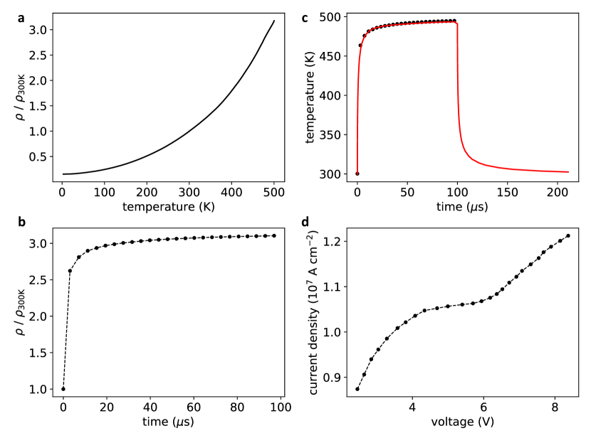
The abrupt resistance drop after the weaker pulse excludes the possibility that the detected high resistance after the first pulse was due to the sample still remaining at an elevated temperature during the readout time. In the Supplementary Information Fig. S2 we show that within a few s after the pulse, the sample cools down back to the base temperature. Our switching signals are therefore detected at times safely exceeding the transient heating time. We estimated from the measured resistivity during the 100 s pulse and from the measured dependence of the resistivity on the base temperature (Supplementary Information Fig. S2) that the temperature of the device during the pulse reaches approximately C, i.e., is around the CuMnAs Néel temperature Wadley2013 .
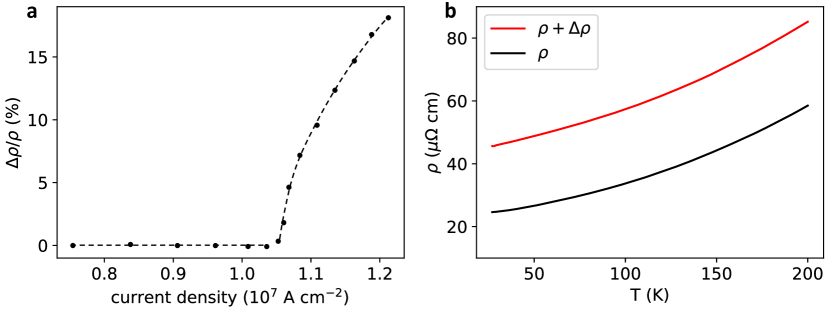
In Fig. 2a we plot the relative size of the quench-switching signal, , obtained directly from a four-point resistivity measurement (see dashed voltage probes in Fig. 1b). The data are plotted for amplitudes of the writing pulses safely below any detectable parasitic electromigration effects (see the discussion of structural characterization below and in the Supplementary Information Sec. II). In all electrical pulsing experiments we use a voltage pulse-source. The voltage-current characteristics for the 100 s writing pulse is shown in Supplementary Information Fig. S2. In Fig. 2a we see no switching signal at lower current amplitudes and an onset followed by an increase with increasing pulse amplitude Shi2020 . In all measurements, the reading current amplitude is well below the onset writing current. The resistive switching ratio approaches 20% at room temperature, i.e., is comparable to the giant-magnetoresistance ratios in ferromagnetic multilayers Chappert2007 .
While at 300 K the metastable high-resistivity state relaxes within a s time-scale, at 200 K the retention time approaches a year (for details see the discussion of Fig. 4). When quench-switching the device by the 100 s writing pulse at 200 K we can therefore perform longer measurements, such as the temperature sweep shown in Fig. 2b, with no relaxation of the written high-resistivity state. By comparing the temperature dependence of the resistivity after applying the writing pulse, , to the resistivity without the pulse, , we see that the switching signal is nearly temperature independent while decreases with decreasing temperature in the metallic CuMnAs. As a result, the switching ratio approaches 100% at low temperatures. We point out that the simple bar-geometry of our devices and their micron-scale lateral size were chosen to highlight the bulk resistivity nature of our quench-switching signals. A comparison of CuMnAs films with thicknesses between 50 and 20 nm further verifies that the signal stems from the bulk of the antiferromagnetic metallic film and not from interface or surface effects.
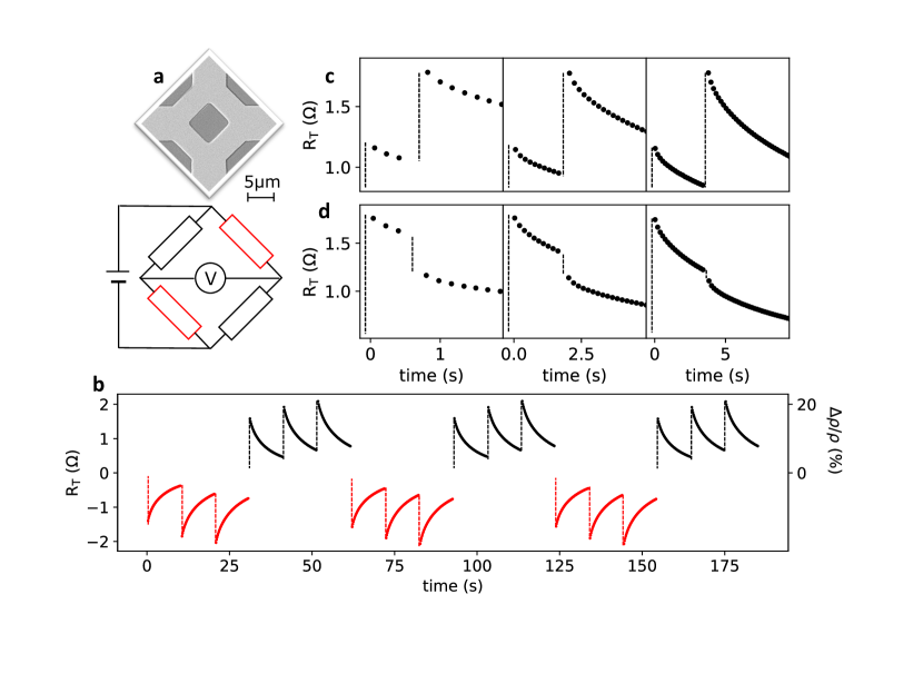
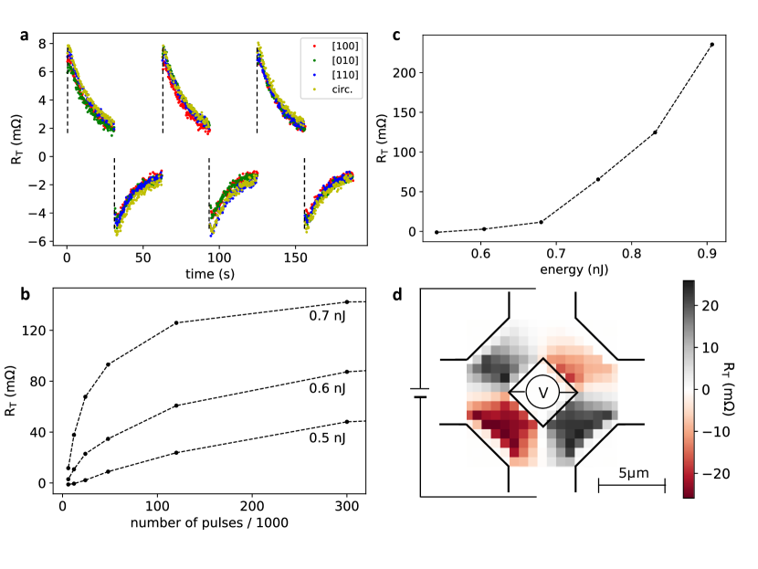
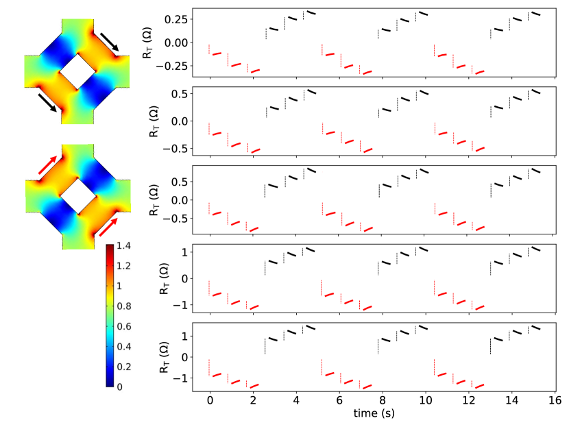
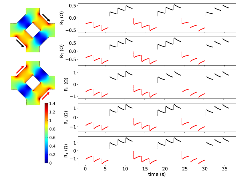
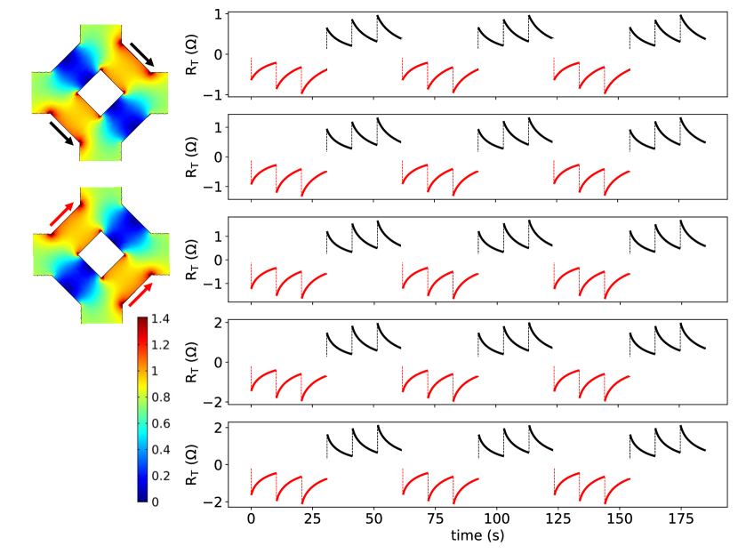
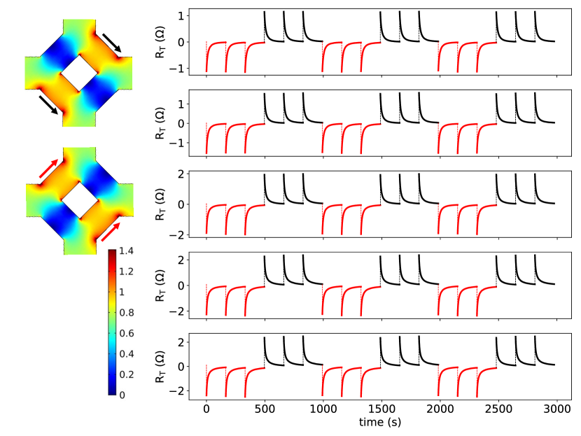
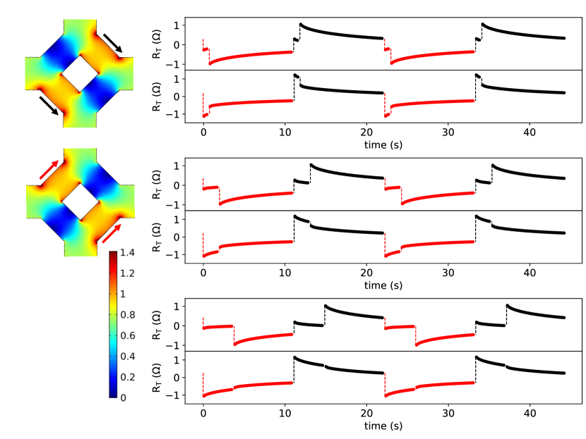
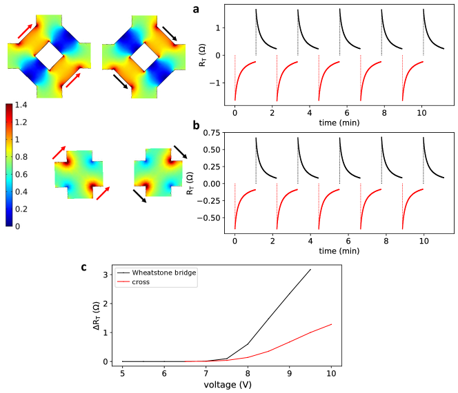
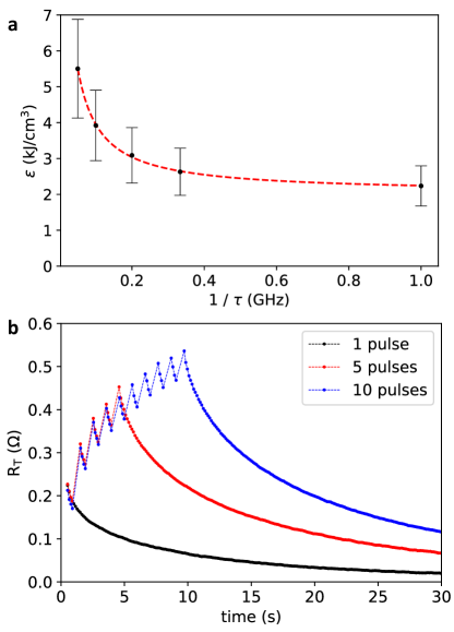
In Fig. 3 we show measurements on a Wheatstone-bridge microdevice which brings several technical advantages over the simple bar geometry. By pulsing the bridge first along one pair and then along the orthogonal pair of resistors and by measuring the bridge resistance (Fig. 3a) we can directly check the reproducibility of the switching signal between different physical resistors while using the same readout probes. Apart from the flipped sign of , which is a geometry effect of the Wheatstone-bridge, the two pairs of resistors show a quantitatively identical switching pattern, as seen in Fig. 3b. This includes the increase of the switching signal with the number of successive pulses of the same amplitude, and the relaxation after each pulse (for more examples see Supplementary Information Figs. S3-7).
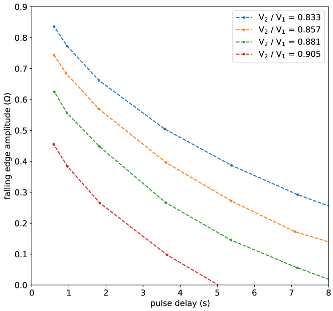
Figs. 3c,d further highlight the analog time-dependent characteristics of our switching signals. When the successive writing pulses have different amplitudes, the written signal can encode the order and delay between the pulses. The presence of a falling edge indicates that the weaker pulse arrived after the stronger pulse and the size of the falling edge decreases with increasing the delay between the two pulses. Supplementary Information Figs. S8,9 highlight the reproducibility and show a more systematic mapping of this analog time-dependent characteristics. We point out that highly reproducible switching characteristics are obtained for different CuMnAs wafers prepared under equivalent growth conditions, and similar switching behavior is also seen in films grown on GaAs or Si over a range of growth parametersKrizek2020 , and in different device geometries (cf. Fig. 1, Fig. S1, Fig. 3, Fig S3-10).
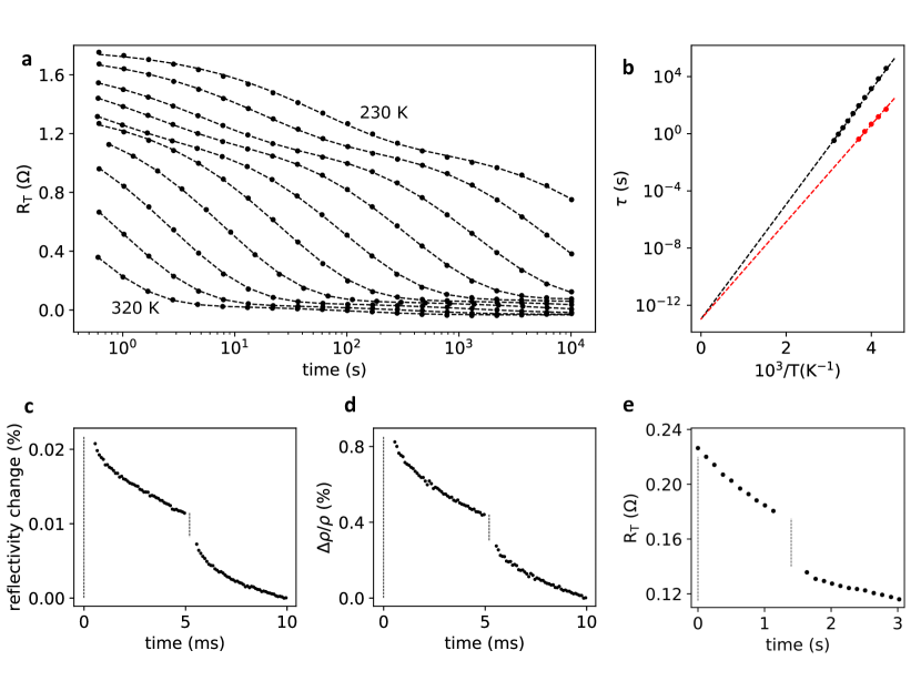
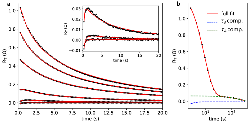
Another advantage of the Wheatstone-bridge geometry is that it removes the temperature dependent offset resistance. (Without applying the switching pulse, the bridge is balanced and .) This allows us to perform low-noise measurements of the switching and subsequent relaxation over times spanning more than four orders of magnitude up to timescales of hours, as shown in Fig. 4a. The observed functional form of the relaxation is universal to all studied temperatures and contains two leading components accurately fitted to Kohlrausch stretched exponentials, , with and two different relaxation times. In theories of relaxation in complex systems, such as glassy materials, where is the dimensionality of the diffusion equation describing the relaxation process Phillips2006 . Our experimental value of corresponds to in the measured 50 nm thick film.
Consistent with theory Phillips2006 , the dependence of the relaxation times on temperature follows a simple exponential, , as seen in Fig. 4b. Here the extrapolated attempt time is within the picosecond range typical of antiferromagnetic dynamics, compared to ferromagnets where it falls into the ns range Aharoni1969 . For the activation energy we obtained K for the slower component and K for the faster component, giving the room-temperature relaxation times in the s and ms ranges, respectively. (For more details on the fitting see Supplementary Information Fig. S11.) We point out that the exponential temperature dependence of the relaxation time explains the unipolar switching from the high to low resistivity state seen in Figs. 1 and 3. During the transient heating of the device due to the weaker pulse, the relaxation of the signal written by the preceding stronger pulse is exponentially accelerated which results in the abrupt falling edge of the signal after the weaker pulse. The resulting signal written by the weaker pulse is lower which reflects the dependence of the size of the signal on the amplitude of the writing pulse (cf. Fig. 2a).
The picture of switching in our devices into complex states, as described by the Kohlrausch model, is consistent with the antiferromagnetic domain nano-fragmentation systematically imaged in our devices by laboratory diamond magnetometryWornle2019 and confirmed by our synchrotron X-ray microscopy which we discuss later in the article. The Kohlrausch relaxation is an example, noted in the past in a range of physical systems, that reproducible and universal behavior can transcend the details of the complex disordered materials and of the measurement probesPhillips2006 . Indeed, we observe high reproducibility of the above switching and relaxation characteristics across different samples and experimental set-ups.
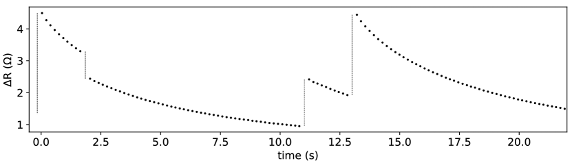
In Figs. 4c,d we demonstrate that our current-induced switching can be probed not only electrically but also optically by measuring the reflectivity change. We again apply the stronger/weaker electrical writing pulse sequence and detect the falling edge. In this experiment we set the delay between the pulses to 5 ms to further illustrate the dynamics of the faster relaxing component () of our switching signal. The short measurement window also allowed us to minimize the noise due to the optical set-up instability in the detection of the weak change in the optical reflectivity. Apart from the smaller amplitude, the optical signal (Fig. 4c) shows the same switching and relaxation pattern as the electrically detected signal (Fig. 4d).
For consistency, we used 100 s writing pulses in all experiments presented so far. Our devices have, however, analogous switching characteristics over the full explored range of current pulse lengths down to 1 ns. This is illustrated in Fig. 4e, again on the stronger/weaker writing pulse sequence and the detection of the falling edge (for more results see Supplementary Information Fig. S12.). We point out that the writing current density in Fig. 4e is lower than in the spin-orbit torque switching by ns-pulses in conventional ferromagnetic devices Baumgartner2017 .
fs-laser pulse switching
To explore the ultimate pulse-length limit we now move in Fig. 5 to the optical switching. In the measurement shown in Fig. 5b we used a nm wavelength laser beam with a 1.7 m spot size and an energy of 1 nJ (30% absorbed) per 100 fs pulse. Using a pulse-picker we select a single 100 fs pulse focused on a single spot on the Wheatstone bridge device (see Fig. 5a). 550 ms after the laser pulse we start recording the electrical readout signal . We then shift the laser spot to the neighboring arm of the Wheatstone bridge and again perform the single-pulse switching measurement. In analogy to the electrical switching, the sign of flips when shifting the spot from one to the neighboring arm and we observe the same relaxation characteristics of the signal. The energy density required for switching by the single fs-laser pulse (kJcm-3) is comparable to the Joule energy density in the electrical switching by a ns-pulse (see Supplementary Information Fig. S12). Since switching is governed by the energy (current) density, our mechanism allows for the device scalability as in the latest generation of ferromagnetic spin-torque memories, and in contrast to the unscalable traditional magnetic recording by the Oersted field proportional to current. We emphasize that our quench-switching mechanism allows us to write, in the same material and device, by a pulse whose length covers the entire range from micro to femtoseconds and that our energy of the laser pulse is lower than in the earlier ultra-fast optical switching experiments in ferrimagnetsKimel2019 .
Next we show that we can optically control the high/low resistance switching as in the unipolar electrical experiment. In the measurement in Fig. 5c we fixed the position of the laser spot in one arm and first applied the 1.7 m focused laser beam with 10 kHz repetition rate over 250 ms. Then we measured for 5 s the readout signal. Next we applied another pulse train in which we defocused the beam to a larger diameter to reduce its maximum energy. We observe the falling edge in the readout signal. In analogy to the electrical switching experiment in Fig. 3, the size of the falling edge depends on the delay between the stronger and the weaker laser pulse, as shown in Figs. 5c,d.
The optical switching we observe is independent of the polarization of the laser pulse, as shown in Fig. 6a. The comparison between Figs. 5b,c also shows that the switching signals after a train of pulses are larger than after a single laser-pulse. The dependence on the number and amplitude of the laser pulses is studied in detail in Figs. 6b,c. Here to facilitate a direct comparison to the amplitudes in the electrical switching measurements, we show the readout signal measured after completing a scan of the laser beam over the entire arm of the Wheatstone-bridge device. Using a pulse-picker, the points in Fig. 6b are obtained with a 600 ms long scanning pulse train while the repetition rate is increased from 10 kHz to 0.5 MHz. The switching signals generated by the optical pulses reach comparably high amplitudes as in the case of electrical pulses. Also in analogy to the electrical writing, we observe a multi-level optical switching but due to the high repetition rates of the laser pulses we can access orders of magnitude higher number of pulses. A single device is exposed to millions of pulses in these optical measurements which, apart from the reproducibility, evidences the endurance of the devices in our switching experiments.
To illustrate the additional spatial resolution allowed by extending our switching mechanism to optical pulses, we plot in Fig. 6d a scanning pixel-by-pixel sequence of optical-writing and electrical-readout in the Wheatstone bridge device. Here each micron-size pixel is exposed to a train of pulses with a 10 kHz repetition rate over 250 ms. Then we record the electrical readout signal and shift the laser spot to the next pixel and repeat the same measurement procedure. As expected, the sign of the signal sharply changes when shifting the spot across the neighboring arms.
The smooth relaxation function we observe in our universal electrical or optical quench-switching is unparalleled in traditional magnetic devices in which the memory loss has a form of stochastic fluctuations between the two equilibrium states with opposite magnetization. Our quench-switching and relaxation functionality can be implemented in analog spiking neuromorphic circuits to mimic the neuron’s leaky integration (Fig. 3b and Figs. S3-7) and to detect the pulse order and delay (Figs. 3c,d and Figs. S8,9) which determine the synaptic weightsWulframGerstner2002 ; Kurenkov2019 . We have demonstrated that, at room temperature, our analog devices can simultaneously operate in two relaxation ranges of milliseconds and seconds. The ranges can be further modified by, e.g., changing the operation temperature. We note that in the alternative magnetic memory concept considered for spiking neuromorphics prior to our workKurenkov2019 , the time-dependence was realized via the extrinsic transient heating by the pulses. This is fundamentally distinct from our mechanism relying on the intrinsic smooth, universal and tunable relaxation from the higher energy metastable states.
Quench-switching mechanism
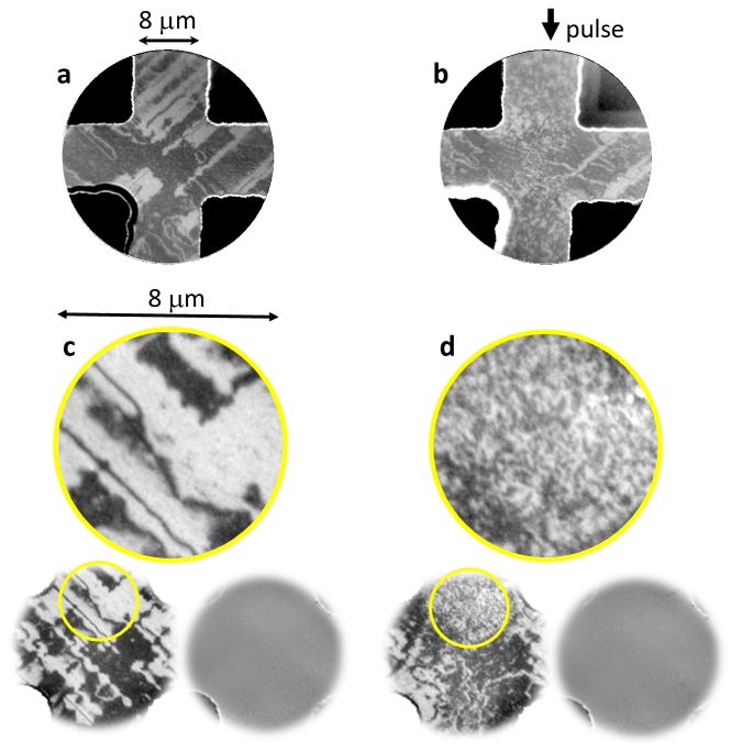
In this section we discuss the microscopic origin of our new switching mechanism. In a parallel study on our CuMnAs devicesWornle2019 , electrical pulsing has been performed simultaneously with a scanning NV-diamond magnetometry of antiferromagnetic domains using a pump-probe scheme. The imaging reveals a nano-scale fragmentation of the antiferromagnetic domains linked to the analog switching signals. The domain fragmentation, which is estimated to reach a 10 nm scale, is controlled by the number and amplitude of the pulses. Images acquired at different pump-probe delays reveal that the fragmented domain pattern maintains a memory of the pristine state towards which it relaxes. These characteristics are mirrored in the multi-level switching and relaxation of the electrical readout signal. An independent confirmation of the pulse-induced fragmentation of antiferromagnetic domains by our XMLD-PEEM measurements is presented in Fig. S14 (see also Methods).
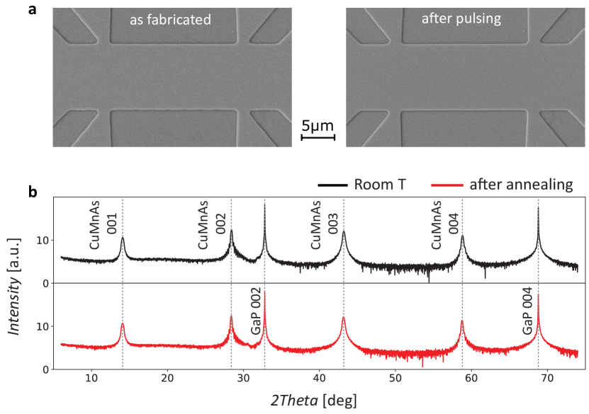
Additionally, a collection of structural characterization measurements has been performed on our samples, some presented in Supplementary Information Figs. S13 and S14, and an extensive set of results summarized in a parallel studyKrizek2020 . The experiments show that the single-crystal CuMnAs epilayers grown with the best substrate matching, stoichiometry, uniformity, and minimized abundance of defects have optimized characteristics of our quench-switching signals. As mentioned above, we experimentally determined that the system heats up to the vicinity of the antiferromagnetic transition temperature during the short writing pulse. In comparison, the range of optimal growth temperatures (190-260∘C) exceeds the Néel temperature and at these high temperatures and for the much longer growth time (tens of minutes) than the pulse length, the synthesized epilayer preserves full crystal order. Our structural characterizations also include scanning electron microscopy (Figs. S13) and X-ray absorption PEEM (Fig. S14) on pulsed devices, transmission electron microscopy on thin lamellae while heated to temperatures exceeding the transient heating in devices during the pulseKrizek2020 , and X-ray diffraction after post-growth annealing of the crystal at these excessive temperatures (Fig. S13). We observe no signs of electromigration or structural transition of the crystal for electric field and heating conditions corresponding to the pulsing experiments reported in our work.
The transition to the metastable nano-fragmented domain state is, on the other hand, firmly established by the two independent magnetic microscopies. The excitation of the antiferromagnet into a fragmented domain state when bringing the system close to the Néel transition point can be readily ascribed to the entropy gain in the free energy Yin-Yuan1956 . Remarkably, our experiments show that the antiferromagnet retains the high resistive nano-fragmented domain state over time scales that exceed by many orders of magnitude the time over which the system is in the transient excited state at elevated temperature.
Regarding the magnitude of the resistive signal we refer, for example, to an earlier study of the striped domain phase of a Co film Gregg1996 where a 5% increase of the resistivity compared to the uniform magnetic state was caused by a density of domain walls about twenty-times lower than the density reached in the present experiments, as inferred from the parallel NV-diamond magnetometry study on our devices Wornle2019 . Resistive changes of 100% in our nano-fragmented state are, therefore, in line with the measurements in ferromagnets when extrapolated to our high domain wall densities. Another comparison is provided by earlier ab initio transport calculations in CuMnAs Maca2017 . Here a relative increase of the resistivity by over 100% was obtained when comparing the resistivity of a material with a given substitutional lattice disorder and a perfect magnetic order to a material with the same lattice disorder and a strong frozen magnetic disorder.
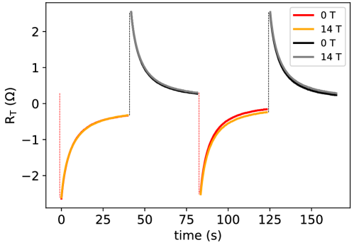
Finally, we remark that in current-polarity dependent switching measurements, the NV-diamond magnetometry study also illustrates a coexistence of the domain fragmentation with the Néel vector reorientation in the antiferromagnetic domains Wornle2019 . The Néel vector reorientation was also directly observed in earlier XMLD-PEEM studiesGrzybowski2017 ; Wadley2018 . From the magnetic imaging and from another parallel study of AMR in CuMnAs in strong magnetic fields Wang2020 we conclude that for the resistive switching ratios on the order of a fraction of a per centWadley2016 ; Olejnik2018 , both AMR due the Néel vector reorientation in the domain and the resistivity increase due to the domain fragmentation can contribute. With increasing amplitude of the resistive readout signal, the domain fragmentation quench-switching takes over. We note that the magnetic-field dependent AMR and XMLD Wang2020 indicate that the reorientation of the Néel vector inside the antiferromagnetic domains can occur at around 2 T while XMLD-PEEM measurementsWang2020 showed that the system remained in a multi-domain state even after applying and removing a 7 T field. Consistently with these microscopies, our large quench-switching signals, ascribed to nano-fragmented multi-domain states, are insensitive to strong magnetic fields (see Supplementary Information Fig. S15 for our measurements in 14 T).
Conclusions
We have reported the quenching of an antiferromagnet into high-resistive nano-fragmented domain states after bringing the system close to the Néel transition point using electrical or ultra-short optical pulses. Key questions do though remain, which are related to the limiting excitation time-scales of the quench-switching process, as well as the scattering mechanism responsible for the high resistivity of the quenched state. Furthermore, the processes that allow a single-crystal epilayer with a collinear antiferromagnetic ground state to remain in the fragmented metastable state for macroscopic timescales are currently unclear. To address these questions, considering the nanoscale fragmentation and the picosecond relaxation attempt times we observe, microscopic imaging techniques with higher spatial and temporal resolution will be needed. Furthermore, since electronic (structural) fluctuation at the nanoscale might accompany the strong magnetic disorder, both charge and spin sensitive imaging will be desirable to elucidate the microscopic origin of the activation energy barriers determining the retention/relaxation time-scale. The quench switching in dipolar-field free antiferromagnets reported here has no counterpart in ferromagnetic systems and could prove to be of value in a range of areas, from unconventional memory-logic devices to ultrafast optical switching.
Methods
Growth. of the films of tetragonal CuMnAs used in this study was done by molecular beam epitaxy at substrate temperatures around 200°C. The films were capped by 3nm of Al layer which, after quick oxidation following removal from vacuum, prevents oxidation of CuMnAsKrizek2020 . To pattern the devices we used electron beam lithography and wet chemical etching: Aluminium cap was removed in 2.7% C4H13NO (3 s) and as the CuMnAs etchant we used a mixture 4:1:2 C4H6O6(5%):H2O2(5%):H2SO4(10%) with the rate of 50 nm per 30 s.
Synchronous electrical and optical readout. (Figs. 4c,d) we performed using a fast NI data acquisition card which recorded simultaneously in one channel electrical resistance and in second channel analog output of a lock-in amplifier monitoring reflected light intensity (modulated by a photoelastic modulator at frequency 100 kHz).
ns electrical pulses. (Fig4e, Fig. S12) we delivered using a custom designed four-terminal high frequency PCB sample holder. The voltage pulses were generated by a specialized pulse generator (Kentech RTV-30 Sub-ns Pulser).
100 fs optical pulses. (Figs. 5,6) were generated by a Ti:sapphire laser. The base repetition rate was 82 MHz and we utilized a pulse picker to obtain lower repetition rates. The wavelength of the laser light was 800 nm, corresponding to energy of 1.55 eV, i.e., well below the band gap of the GaP substrate (2.26 eV).
Photo-emission electron microscopy (PEEM) images. (Fig. S14) were obtained on beamline I06 at Diamond Light Source, using an Elmitec SPELEEM-III microscope to image secondary-electron emission arising from X-rays incident on the sample at a grazing angle of 16∘. The probe depth was nm, and the lateral resolution was nm. A pulsing power supply was connected to the sample in ultrahigh vacuum via feedthroughs to the sample holder. Magnetic contrast images were obtained using the X-ray magnetic linear dichroism (XMLD) asymmetry, which measures the local surface Néel vector. We acquired images for each X-ray energy during 1s exposure times, and we averaged 20 images to obtain a single XMLD-PEEM image. For more details see Ref. Wadley2018, .
Data availability statement. The data that support the plots within this paper and other findings of this study are available from the corresponding author upon reasonable request.
References
- (1) Neel, L., Néel, L., Neel, L. & Néel, L. Magnetism and Local Molecular Field. Science 174, 985–992 (1971).
- (2) Shick, A.B., Khmelevskyi, S., Mryasov, O.N., Wunderlich, J. & Jungwirth, T. Spin-orbit coupling induced anisotropy effects in bimetallic antiferromagnets: A route towards antiferromagnetic spintronics. Physical Review B 81, 212409 (2010).
- (3) Park, S.R., Kim, C.H., Yu, J., Han, J.H. & Kim, C. Orbital-angular-momentum based origin of rashba-type surface band splitting. Physical Review Letters 107, 156803 (2011).
- (4) Chen, H., Niu, Q. & Macdonald, A.H. Anomalous Hall effect arising from noncollinear antiferromagnetism. Physical Review Letters 112, 017205 (2014).
- (5) Nakatsuji, S., Kiyohara, N. & Higo, T. Large anomalous Hall effect in a non-collinear antiferromagnet at room temperature. Nature 527, 212–215 (2015).
- (6) Železný, J. et al. Relativistic Néel-order fields induced by electrical current in antiferromagnets. Physical Review Letters 113, 157201 (2014).
- (7) Wadley, P. et al. Electrical switching of an antiferromagnet. Science 351, 587–590 (2016). eprint 1503.03765.
- (8) Železný, J., Wadley, P., Olejník, K., Hoffmann, A. & Ohno, H. Spin transport and spin torque in antiferromagnetic devices. Nature Physics 14, 220–228 (2018).
- (9) Bodnar, S.Y. et al. Writing and reading antiferromagnetic Mn2Au by Néel spin-orbit torques and large anisotropic magnetoresistance. Nature Communications 9, 348 (2018).
- (10) Jungwirth, T., Marti, X., Wadley, P. & Wunderlich, J. Antiferromagnetic spintronics. Nature Nanotechnology 11, 231–241 (2016).
- (11) Baltz, V. et al. Antiferromagnetic spintronics. Reviews of Modern Physics 90, 015005 (2018).
- (12) Jungwirth, T. et al. The multiple directions of antiferromagnetic spintronics. Nature Physics 14, 200–203 (2018).
- (13) Němec, P., Fiebig, M., Kampfrath, T. & Kimel, A.V. Antiferromagnetic opto-spintronics. Nature Physics 14, 229–241 (2018).
- (14) Šmejkal, L., Mokrousov, Y., Yan, B. & MacDonald, A.H. Topological antiferromagnetic spintronics. Nature Physics 14, 242–251 (2017).
- (15) Gomonay, O., Baltz, V., Brataas, A. & Tserkovnyak, Y. Antiferromagnetic spin textures and dynamics. Nature Physics 14, 213–216 (2018).
- (16) Daughton, J.M. Magnetoresistive memory technology. Thin Solid Films 216, 162–168 (1992).
- (17) Wadley, P. et al. Current polarity-dependent manipulation of antiferromagnetic domains. Nature Nanotechnology 13, 362–365 (2018).
- (18) Wang, M. et al. Spin flop and crystalline anisotropic magnetoresistance in CuMnAs. Physical Review B 101, 094429 (2020).
- (19) Chappert, C., Fert, A. & Van Dau, F.N. The emergence of spin electronics in data storage. Nature Materials 6, 813–823 (2007).
- (20) Kimel, A.V. & Li, M. Writing magnetic memory with ultrashort light pulses. Nature Reviews Materials 4, 189–200 (2019).
- (21) Wörnle, M.S. et al. Current-induced fragmentation of antiferromagnetic domains (2019). URL http://arxiv.org/abs/1912.05287.
- (22) Wadley, P. et al. Tetragonal phase of epitaxial room-temperature antiferromagnet CuMnAs. Nature Communications 4, 2322 (2013).
- (23) Krizek, F. et al. Molecular beam epitaxy of CuMnAs. Physical Review Materials 4, 014409 (2020).
- (24) Shi, J. et al. Electrical manipulation of the magnetic order in antiferromagnetic PtMn pillars. Nature Electronics 3, 92–98 (2020).
- (25) Phillips, J.C. Axiomatic theories of ideal stretched exponential relaxation. Journal of Non-Crystalline Solids 352, 4490–4494 (2006).
- (26) Aharoni, A. Effect of a Magnetic Field on the Superparamagnetic Relaxation Time. Phys. Rev. 177, 793 (1969).
- (27) Baumgartner, M. et al. Spatially and time-resolved magnetization dynamics driven by spin-orbit torques. Nature Nanotechnology 12, 980–986 (2017).
- (28) Gerstner, W. & Kistler, V.M. Spiking Neuron Models (Cambridge University Press, 2002).
- (29) Kurenkov, A. et al. Artificial Neuron and Synapse Realized in an Antiferromagnet/Ferromagnet Heterostructure Using Dynamics of Spin-Orbit Torque Switching. Advanced Materials 31, 1900636 (2019).
- (30) Li, Y.Y. Domain Walls in Antiferromagnets and the Weak Ferromagnetism of Fe2O3. Physical Review 101, 1450–1454 (1956).
- (31) Gregg, J.F. et al. Giant Magnetoresistive Effects in a Single Element Magnetic Thin Film. Physical Review Letters 77, 1580–1583 (1996).
- (32) Máca, F. et al. Physical properties of the tetragonal CuMnAs: A first-principles study. Physical Review B 96, 094406 (2017).
- (33) Grzybowski, M.J. et al. Imaging Current-Induced Switching of Antiferromagnetic Domains in CuMnAs. Physical Review Letters 118, 057701 (2017).
- (34) Olejník, K. et al. Terahertz electrical writing speed in an antiferromagnetic memory. Science Advances 4, eaar3566 (2018).
Acknowledgements
We acknowledge Jiří Kastil and Martin Míšek for experimental support. This work was supported in part by the Ministry of Education of the Czech Republic infrastructures Grants CzechNanoLab No. LM2018110, No. LNSM-LNSpin and MGLM No. LM2018096, the Czech Science Foundation Grant No. 19-28375X, the Charles University Grant GA UK No. 886317 and 1582417, the EU FET Open RIA Grant No. 766566, the Engineering and Physical Sciences Research Council Grant No. EP/P019749/1. P.W. acknowledges support from the Royal Society through a University Research Fellowship. T.J acknowledges the support from the Neuron Foundation Prize, and K.O. form the Neuron Foundation Impuls Grant.
Author Contributions
Author contributions: K.O., Z.K., and T.J. conceived and designed the project. Z.K., M.S., J.Z., F.K., K.O., P.W., K.W.E., S.R., O.J.A., F.M., and S.S.D. performed experiments. K.O., P.N., P.W., K.W.E., J.W., X.M., M.S.W, P.G., and T.J. analyzed data. V.N., F.K., and R.P.C. contributed materials. K.O. and T.J. wrote the paper.
Competing interests
The authors declare no competing interests.
Additional information
Supplementary Information is available for this paper at https://doi.org/10.1038/s41928-020-00506-4.
Reprints and permissions information is available at www.nature.com/reprints.
Correspondence and requests for materials should be addressed to K.O. and T.J.
Figures
Supplementary Note 1
Electrical switching
This section contains supplementary figures on analog switching characteristics for 100 s electrical pulses (Figs. S1, S3-S10), temperature rise during the pulse and current-voltage characteristic (Fig. S2), fitting of the time and temperature dependent relaxation (Fig. S11), and switching by 1 ns electrical pulses with comparison of switching energies for ns-electrical and fs-laser pulses (Fig. S12).

Supplementary Note 2
Structural characterization and magnetic imaging
This section contains figures with scanning electron micrographs of devices before and after pulsing and X-ray diffraction of films before and after annealing (Fig. S13), and X-ray absorption PEEM and XMLD-PEEM images of devices before and after pulsing (Fig. S14). Below we also discuss parasitic effects reported elsewhere in sputtered Pt/insulator bilayers.
Several papers have recently reported parasitic pulse-induced resistive changes in Pt-(antiferromagnetic)insulator bilayers with few-nm thick Pt filmsChiang2019 ; Zink2019 ; Zhang2019c ; Baldrati2019 ; Cheng2020 ; Churikova2020 These parasitic signals, typically of a fraction of per cent amplitude, are linked to the well-established elecromigration effects promoted at grain boundaries in microdevices of sputtered thin metal filmsKozlova2013 . A Viewpoint articleZink2019 on Ref. Chiang2019, emphasizes that the possible occurrence of parasitic effects in these samples highlights the importance of direct imaging of the magnetic switching in the insulating antiferromagnet.
In contrast to the above studies, we use a single-crystal metallic antiferromagnet CuMnAs grown by molecular beam epitaxy. The switching to the metastable nano-fragmented antiferromagnetic domain state in our devices was verified by a parallel systematic laboratory study employing the NV-diamond microscopy Wornle2019 , and by our independent synchrotron XMLD-PEEM measurements (Supplementary Fig. S14). Previous XMLD-PEEM measurements in CuMnAs also provided direct images of the earlier mechanism of the Néel vector reorientation controlled by the current directionWadley2018 .
The absence of detectable structural transitions is discussed in the main text, evidenced here in Supplementary Fig. S13 and S14, and in an extensive parallel studyKrizek2020 . The magnetic transition to the metastable nano-fragmented domain state is, on the other hand, firmly established by the magnetic microscopies. Regarding the magnitude of the corresponding resistive signal we refer in the main text to the consistency with earlier domain wall resistance studies in ferromagnetsGregg1996 and ab initio transport calculations in CuMnAsMaca2017 . We also recall from the main text that we performed, in the same material and device structure, electrical and optical switching experiments with pulses covering the nine orders of magnitude range from microseconds to femtoseconds and that we observed precisely reproducible relaxation of the metastable state with attempt times in the picosecond range, consistent with the internal dynamics scale of antiferromagnets.
Unlike the claims in Ref. Chiang2019, on their experiments on sputtered polycrystalline Pt-insulator structures, we experimentally excluded the possibility that our signals are due transient heating induced by the writing pulse and persisting during readout. First evidence is the resistance drop after the weaker pulse (Figs. 1-4 in the main text and Supplementary Figs. S1 and S8), i.e., that we can deterministically control the switching towards not only the high but also the low resistivity states by the pulse amplitude. Second, we showed in Supplementary Fig. S2 that within a few s after the s pulse, the sample cools down back to the base temperature. Our switching signals are therefore detected at times safely exceeding the transient heating time.
Supplementary Note 3
Switching in the presence of strong magnetic fields
References
- (1) Wadley, P. et al. Current polarity-dependent manipulation of antiferromagnetic domains. Nature Nanotechnology 13, 362–365 (2018).
- (2) Chiang, C. C., Huang, S. Y., Qu, D., Wu, P. H. & Chien, C. L. Absence of Evidence of Electrical Switching of the Antiferromagnetic Néel Vector. Physical Review Letters 123, 227203 (2019).
- (3) Zink, B. The Heat in Antiferromagnetic Switching. Physics 12, 134 (2019).
- (4) Zhang, P., Finley, J., Safi, T. & Liu, L. Quantitative Study on Current-Induced Effect in an Antiferromagnet Insulator/Pt Bilayer Film. Physical Review Letters 123, 247206 (2019).
- (5) Baldrati, L. et al. Mechanism of Néel Order Switching in Antiferromagnetic Thin Films Revealed by Magnetotransport and Direct Imaging. Physical Review Letters 123, 177201 (2019).
- (6) Cheng, Y., Yu, S., Zhu, M., Hwang, J. & Yang, F. Electrical Switching of Tristate Antiferromagnetic Néel Order in alpha Fe2O3Epitaxial Films. Physical Review Letters 124, 027202 (2020).
- (7) Churikova, A. et al. Non-magnetic origin of spin Hall magnetoresistance-like signals in Pt films and epitaxial NiO/Pt bilayers. Applied Physics Letters 116, 022410 (2020).
- (8) Kozlova, T., Rudneva, M. & Zandbergen, H. W. In situ TEM and STEM studies of reversible electromigration in thin palladium-platinum bridges. Nanotechnology 24, 505708 (2013).
- (9) Wörnle, M. S. et al. Current-induced fragmentation of antiferromagnetic domains (2019).
- (10) Krizek, F. et al. Molecular beam epitaxy of CuMnAs. Physical Review Materials 4, 014409 (2020).
- (11) Gregg, J. F. et al. Giant Magnetoresistive Effects in a Single Element Magnetic Thin Film. Physical Review Letters 77, 1580–1583 (1996).
- (12) Máca, F. et al. Physical properties of the tetragonal CuMnAs: A first-principles study. Physical Review B 96, 094406 (2017).