listing
Streaming Message Interface: High-Performance Distributed Memory Programming on Reconfigurable Hardware
Abstract.
Distributed memory programming is the established paradigm used in high-performance computing (HPC) systems, requiring explicit communication between nodes and devices. When FPGAs are deployed in distributed settings, communication is typically handled either by going through the host machine, sacrificing performance, or by streaming across fixed device-to-device connections, sacrificing flexibility. We present Streaming Message Interface (SMI), a communication model and API that unifies explicit message passing with a hardware-oriented programming model, facilitating minimal-overhead, flexible, and productive inter-FPGA communication. Instead of bulk transmission, messages are streamed across the network during computation, allowing communication to be seamlessly integrated into pipelined designs. We present a high-level synthesis implementation of SMI targeting a dedicated FPGA interconnect, exposing runtime-configurable routing with support for arbitrary network topologies, and implement a set of distributed memory benchmarks. Using SMI, programmers can implement distributed, scalable HPC programs on reconfigurable hardware, without deviating from best practices for hardware design.
This is a preprint version..
1. Introduction
The end of Moore’s law and Dennard scaling causes a major disruption to the high-performance computing industry. Both require us to re-think computer architecture in order to reduce data movement and power dissipation on chips, and to use the existing transistors more efficiently. To address both problems, reconfigurable architectures with application-specific dataflow as well as compute logic provide a viable option. Many large-scale datacenter operators, such as Amazon (instances, [n. d.]) and Microsoft (Chung et al., 2018), already build on reconfigurable logic to specialize hardware implementations to their workloads. Reconfigurable logic can avoid the well-known architectural von Neumann (load-store) bottleneck, but poses new challenges in programming these devices. Yet, highly efficient designs with significant performance and energy benefits have shown that efforts in the area are well spent (Kara et al., 2017; Zhang et al., 2016; Umuroglu et al., 2017).
Reconfigurable hardware traditionally came in the flavor of fully configurable logic devices, field-programmable gate arrays (FPGAs), or devices with a large fraction of hardened logic with flexible datapaths, so-called coarse-grained reconfigurable arrays (CGRAs). Today, the boundary between FPGAs and CGRAs is vanishing, with the introduction of high-performance FPGAs that contain powerful DSP cores, such as Intel’s Stratix 10 ( single precision (Table, [n. d.]a)), and AI Engines in Xilinx Versal devices (Table, [n. d.]b). Those high-performance FPGAs become highly attractive for HPC workloads if the programming problem can be solved. Recent developments in high-level synthesis promises to deliver high productivity on FPGAs replacing the traditional register transfer logic (RTL) specification with a standard C/C++ code interface integrated with modern OpenCL frameworks (Czajkowski et al., 2012; Cong et al., 2011).
Most of the HLS research focuses on programming one or multiple FPGAs attached to a single host. Yet, in HPC systems, single FPGAs need to be scaled up to clusters containing many devices. Today, communication is performed through message passing at the host, where data is usually transported via PCI Express (PCIe) to the main memory, and then through a different PCIe channel to the network interface. This adds high overheads in terms of latency, bandwidth, and load on the host’s memory subsystem. Nearly all modern FPGA chips bear high-performance serial link network connections. For example, Intel’s Stratix 10 chip has four connections and Xilinx’ UltraScale+ chips support off-chip connectivity. These links are often available via proprietary interfaces for communication among directly connected FPGAs. Unfortunately, no distributed memory programming model exists for HLS-programmed devices, and programmers are forced to resort to licensed IP cores and RTL designs to implement FPGA-to-FPGA communications (Owaida and Alonso, 2018; Kobayashi et al., 2018).
We propose a distributed memory HLS programming model for FPGAs that provides the convenience of message passing for HLS-programmed hardware devices. While we cannot simply use the Message Passing Interface (MPI) API due to the peculiarities of programmed hardware, we are heavily inspired by MPI’s interface, to benefit from its proven effectiveness in practice, and maintain familiarity for programmers. The reason for this specialization is that high-performance HLS designs are deeply pipelined and vectorized. This means that several results are produced at each clock cycle and shallow buffering along predefined (pipeline) paths is a necessity for performance. Thus, our Streaming Message Interface (SMI) does not assume that buffers are first computed and then communicated—instead, sending a message is integrated into the pipeline. The key concept of SMI is its streaming nature, where a send or receive is set up first, and the data is then written or read on a cycle-by-cycle basis. This concept modifies MPI-style messages into transient channels, that have similar semantics, but integrate seamlessly with HLS-programmed pipelines.
The key contributions of our work are:
-
•
We propose the streaming messages communication model, unifying the message passing and streaming models;
-
•
We design the Streaming Message Interface (SMI), an HLS communication interface specification for programming streaming messages in distributed memory multi-FPGA systems;
-
•
We implement and benchmark a reference implementation of SMI that integrates with OpenCL on Intel FPGAs;
-
•
We release the reference library and example applications implemented with a modern HLS tool as open source code that does not rely on additional licensed IP cores.
We evaluate our approach on several numerical computations, showing the performance benefits of distributed memory FPGA programming, by increasing available compute resources and memory bandwidth.
2. Programming FPGA Communication
To design a suitable communication model for distributed FPGA programming, we wish to learn from the most prominent model found in HPC, namely message passing (specifically, MPI), but adapt it to a form suitable for hardware programming. We call our model streaming messages, and will introduce it by highlighting the gaps in existing models, which it has been designed to fill.
Programming FPGAs with high-level synthesis revolves around designing deep hardware pipelines, exploiting the spatially parallel nature of the FPGA fabric. Parallelism is achieved by making this pipeline deeper (pipeline parallelism), by making the pipeline wider (vector parallelism), or by replicating the pipeline entirely (task parallelism) (de Fine Licht et al., 2018). Pipelines are expressed as loops in the HLS code, designed such that new operands can be accepted every cycle. It is thus imperative that a communication model is compatible with this programming model, allowing communication to happen during pipelined computations.
2.1. Existing Communication Models
2.1.1. Message Passing
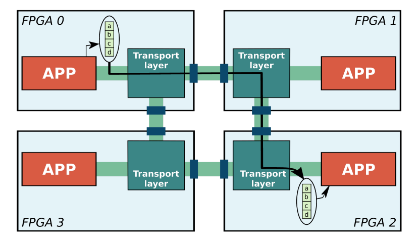
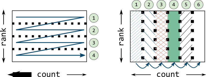
The paradigm of message passing uses local buffers to both send and receive information to/from other processes (called ranks). A distributed algorithm will work on a local subset of data on each rank, then indicate to the communication layer when a buffer is ready to be sent to another rank, or when it is ready to receive new data into a buffer. This is illustrated with an example code in Fig. 4, where a buffer is populated in a loop, then sent to another rank. To hide communication time, message passing uses non-blocking calls to overlap communication and computation, thus letting ranks operate on different data than what is currently being exchanged.
In the context of hardware programming, message passing has two key shortcomings. First, the model relies on bulk transfers, which is a poor match to the HLS programming model, as we wish to communicate during pipelined computation. Second, bulk transfers imply large buffers required to store intermediate data. On the CPU, these buffers exist in the global memory space, and can dynamically move between cache and DRAM, depending on their size and the behavior of the program. In contrast, buffers used when programming for hardware are explicitly instantiated in a fast memory distributed across the chip, and moving them to an off-chip memory requires explicit wiring to limited DRAM interfaces, which are shared among all accesses. Fully adapting this approach in hardware would thus come with significant disadvantages in resource utilization, programmability, and performance.
2.1.2. Streaming
A classical way of moving data between FPGAs is to simply stream it across an inter-FPGA channel in a pipelined fashion (e.g., the Maxeler dataflow engine architecture (Dimond et al., 2011)), similar to how data is moved across the chip on a single FPGA. This approach offers a way of expressing communication that is natural to the hardware paradigm, by pushing data to the output interface in a pipelined fashion during processing (see Fig. 4). Streaming relies on point-to-point connections known at configuration time, suitable for extending one-dimensional systolic array-style architectures across multiple chips (Sano et al., 2014).
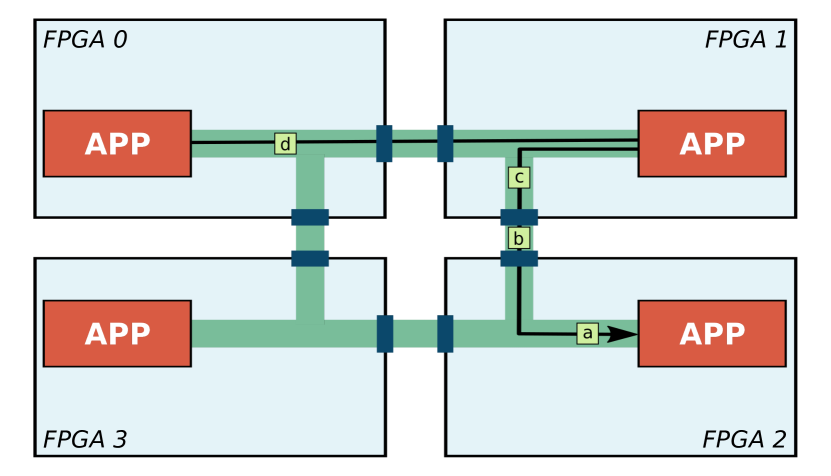
The major shortcoming of streaming interfaces in a distributed memory setting is the lack of flexibility in the implied API and transport layer. Even if the target platform has the necessary hardware ports, a shell that exposes them, and an API to access them, moving data from a given source to a given destination requires the programmer to construct the exact path that the data has to move across as part of the architecture. This has to be repeated for every desired communication channel, for every target application; including forwarding logic when multiple hops are required, and arbitration between different channels using the same hardware connection. In the example shown in Fig. 4, data travelling from FPGA 0 to FPGA 2 must first be sent through FPGA 1, where custom user logic must take care of forwarding it to the final destination. For more complicated distributed memory environments, the streaming interface in its pure form is thus insufficient to productively express arbitrary communication patterns.
2.2. Streaming Messages
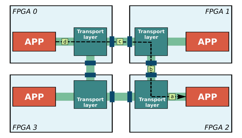
To capture the key ideas of message passing and streaming, while addressing the gaps in both outlined above, we introduce streaming messages: an HPC-oriented communication model for hardware programming, with an implied transport layer. Streaming messages replace traditional, buffered messages with pipeline-friendly transient channels, offering a streaming interface to the hardware programmer, but with the flexibility known from the message passing paradigm. Knowledge of the interconnect topology is not required at compile-time: channels between endpoints are transiently established, where source and destination ranks can be specified dynamically. This is illustrated in Fig. 4, where a kernel on rank 0 on opens a channel to rank 2 on , using port 0 to distinguish the target application (akin to starting a non-blocking send in MPI, but without implying that the data is ready), then pushes data to the channel during processing in a pipelined fashion (as in the streaming paradigm). Routing data to the destination is then handled transparently by the transport layer.
In streaming messages, a rank is associated with a coarse hardware entity assigned to dedicated communication logic, connected to the incoming and outgoing hardware communication ports. A port uniquely identifies an endpoint within a rank, and implements a hardware streaming interface for every Push and Pop operation present in the code to/from a matching external port. This implies that all ports must be known at compile time, such that, within each rank, the necessary hardware connections between the communication endpoints and the network can be instantiated. Ports must be specified both for point-to-point and collective communication primitives to establish the required hardware. All ports represent hardware connections, and can thus operate fully in parallel.
Channels can be programmed either in a single program, multiple data (SPMD) fashion, or in a multiple program, multiple data (MPMD) fashion. In this work, we assume a single rank per FPGA. Ranks involved in communication and the total number of ranks can then be dynamically altered without recompiling the program, by simply updating the routing configuration at each rank.
3. Streaming Message Interface
To concretize the concept of streaming messages, we introduce the Streaming Message Interface (SMI), a communication interface specification for HLS programs inspired by MPI (Message Passing Interface Forum, 2015). SMI is not an implementation, and merely implies the functionality that must be supported by the transport layer to support the interface specification. The interface exposes primitives for both point-to-point and collective communications.
3.1. Point-to-Point Communication
Point-to-point communication in SMI codes is based on transient channels: when established, a streaming interface is exposed at the specified port at either end, allowing data to be streamed across the network using FIFO semantics, with an optional finite amount of buffer space at each endpoint. A streaming message consists of one or more elements with a specified data type. The communication endpoints are uniquely identified by their rank. Ranks uniquely identify FPGA devices, and ports distinguish distinct communication endpoints within a rank.
The example in Lst. 5 shows an MPMD application composed of two ranks implemented with SMI (for code examples, we use the Intel FPGA OpenCL directive syntax, where pragmas apply to the following scope). Rank 0 streams a message of integer elements to Rank 1 using a send channel. Rank 1 opens a receive channel to receive the message, and applies a computation on each data item. Input and output channels are opened before the beginning of the loop, and messages are received and sent one-by-one during computation. Channels are thus accessible with a streaming cycle-by-cycle interface: computations can Push or Pop data to/from a communication channel, one data element per clock cycle.
3.1.1. Point-to-Point Communication API
The user can declare a send or receive channel by specifying the number of elements to send, the data type of the elements, the source or destination rank, the port, and the communicator. Once established, channels exist in code in the form of channel descriptors. Channels are implicitly closed when the specified number of elements have been sent or received.
Analogously to MPI, communicators can be established at runtime, and allow communication to be further organized into logical groups. Channels can also be used to communicate between two applications that exist within the same rank using matching ports. To send and receive data elements from within the pipelined HLS code, SMI provides the SMI_Push and SMI_Pop primitives:
Both functions operate on a channel descriptor from a previously opened channel, and a pointer either to the data to be sent, or to the target at which to store the data. These primitives are blocking, such that SMI_Push does not return before the data element has been safely sent to the network, and the sender is free to modify it, and SMI_Pop returns only after the output buffer contains the newly received data element.
To respect the streaming message model, SMI_Push and SMI_Pop must be implemented in such a way that: i) data elements are sent and received in the same order specified by the user, and ii) calling them can be pipelined to a single clock cycle, such that they can be used in pipelined loops without impairing the initiation interval. Additionally, the type specified by the SMI_Push/SMI_Pop operations must match the ones defined in the Open_Channel primitives. With these primitives, communication is programmed in the same way that data is normally streamed between intra-FPGA modules.
3.2. Collective Communication
Collective communication in MPI is key to develop distributed applications that can scale to a large number of nodes. In collective operations, all ranks in a given communicator must be involved in communicating data. SMI defines the Bcast, Reduce, Scatter, and Gather collective operation primitives analogous to their MPI counterparts.
Each collective operation defined by SMI implies a distinct channel type, open channel operation, and communication primitive. The example in Lst. 6 shows an SPMD application in which the root rank broadcasts the locally produced elements to the other ranks in the communicator.
To perform a Bcast, each rank opens a broadcast-specific channel (SMI_BChannel), indicating the count and data type of the message elements, the rank of the root, the port, and the communicator:
To participate in the broadcast operation, each rank will use the associated primitive (analogous to SMI_Push and SMI_Pop for Send and Recv, respectively):
If the caller is the root, it will push the data towards the other ranks. Otherwise, the caller will pop data elements from the network. Similarly, to perform a Reduce, the associated channel must be opened, indicating the reduction operation to perform, such as SMI_ADD, SMI_MAX, or SMI_MIN:
Data communication occurs with the primitive:
Each rank sends its contribution (data_snd), while the reduced result is produced to the root rank (data_rcv).
SMI allows multiple collective communications of the same type to execute in parallel, provided that they use separate ports. We leave out the interfaces for Scatter and Gather, as they follow the same scheme as presented above.
3.3. Buffering and Communication Mode
SMI channels are characterized by an asynchronicity degree , meaning that the sender can run ahead of the receiver by up to data elements. If the sender tries to push the -th element before an element is popped by the receiver, the sender will stall. The concrete implementation of these buffers can use any form of on-chip memory. Because of this asynchronicity, an SMI send is non-local: it can be started whether or not the receiver is ready to receive, but its completion may depend on the receiver, if the message size is larger than . Correctness of the communication in a distributed setting must be guaranteed by the user, i.e., ensuring that there are no cyclic dependencies between sends and receives that allow deadlocks, and that the program will terminate even if the system provides no buffering.
If the channel asynchronicity degree is bigger or equal than the message size, we suggest to use an eager protocol to transfer data for efficient point-to-point communication: elements can be pushed into the network without first performing a handshake with the receiver, aided by buffers at either endpoint. This saves costly round-trip latencies, improving the efficiency of small messages. Creating a new channel is thus a zero-overhead operation, as this merely instructs the transport layer where data should be sent. The network interfaces must be able to handle stalling and backpressure to safely enable eager communication. On the other hand, if the buffer size is smaller than the message size, a transmission protocol with credit-based flow control must be used between the two application endpoints, to guarantee that the communication occurring on a transient channel will not block the transmission of other streaming messages.
For streaming collective operations, even with sufficiently large buffers, we cannot rely on backpressure and flow control alone to coordinate senders and receivers. With streaming messages, we exploit that data is produced, communicated, and consumed in a pipelined fashion, such that we can rely on small intermediate storage in the FPGA fast memory to buffer parts of the message during computation. However, when data can arrive from a dynamic number of other ranks to a single root FPGA (all-to-one), or when multiple collectives are used in succession, some ranks can run ahead of others. In these scenarios, data can arrive at the receiver side (the root in all-to-one, or any rank in one-to-all) in arbitrary order. Because of limited buffer space, the root cannot reorder the data for a dynamic number of ranks and number of elements. Consider, for example, a Gather without any coordination: rank could send its full contribution to the root before rank , which the root would be unable to reorder for arbitrary message sizes.
To ensure correctness in collective primitives, we employ different synchronization protocols, depending on the type of communication used. For one-to-all collectives (i.e., Bcast and Scatter), ranks must communicate to the root when they are ready to receive before the root starts streaming data across the network, to prevent mixing of data from subsequently opened transient channels using the same port. For all-to-one collectives (Reduce and Gather), the root rank must communicate to each source rank when it is ready to receive the given sequence of data. For Bcast, Scatter, and Gather, synchronization is done once per rank, before all data elements from the given rank can be sent. For Reduce, the root synchronizes with all ranks per tile of reduced elements. This is illustrated for Scatter/Gather and Reduce, respectively, in Fig. 7.
In Gather/Scatter, each rank will send/receive count elements in sequence, only when allowed by the matching rank (i.e., the root for Gather or a non-root rank for Scatter). The communication between the root and the different ranks are performed in sequential order (shown with arrow and numbers in Fig. 7). For Reduce, the root must receives the first sequence of element from all ranks (in any order, given the associativity and commutativity properties of the reduction operation), before receiving the next sequence from all ranks. All the ranks can stream their contributions in parallel (fill columns in Fig. 7) for the current tile being reduced (horizontal width of columns), to the root. The root communicates to all the other ranks when they can start sending the data for the next tile.
As participating in collective operations is parallel with the number of distinct ports, multiple collectives can perform their rendezvous and communication concurrently.
4. Reference Implementation
We present a proof-of-concept implementation of SMI, where the transport layer and all communication primitives are implemented as HLS code, targeting the Intel FPGA SDK for OpenCL (Czajkowski et al., 2012). Network connections are implemented using I/O channels in the SDK, which are mapped to physical interfaces implemented by the board support package (BSP) specifying the FPGA shell, provided by the board vendor. SMI as an interface specification is platform independent, but as the transport layer relies on many platform-specific features, we focus on the Intel infrastructure here.
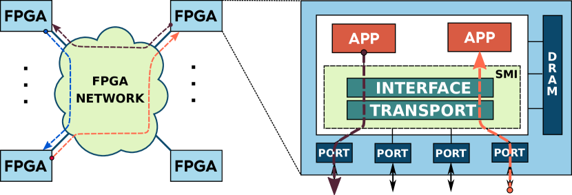
4.1. General Architecture
The SMI implementation resides between applications and the network ports exposed by the FPGA board (see Fig. 8). It is composed of two components: the interface, which implements the SMI primitives described in Sec. 3, and a transport component, which handles data transfer between endpoints.
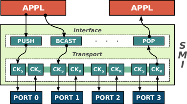
At the SMI application interface, messages are packaged in network packets, which have a size equal to the width of the I/O interface to the network provided by the BSP (e.g., for the experimental platform used). The network packet is the minimal unit of routing, and it may contain one or more data elements. The transport component receives network packets both from the interface and from the network (through the BSP network interfaces). The packet is immediately forwarded onto one of the output links according to the specified target rank and port. The transport layer can accept one new network packet, either coming from the network or from the applications, every clock cycle. With the exception of the routing metadata, no bulk data needs to be buffered in the transport layer, and the transmission of a message is fully pipelined across the network.
4.2. Data Forwarding
Each data communication to/from the network involves moving the data between applications and the transport component through physical hardware connections configured on the FPGA. These connections are implemented using FIFO buffers, where the internal buffer size is a compile-time parameter. This buffer size can be tweaked according to the expected length of the messages that will be sent, taking available FPGA resources into account. By increasing the buffer size, a sending rank can commit more data to the network while continuing computations, which can in some cases improve the overall runtime. This is considered an optimization parameter, as programs must not rely on these buffer sizes for correctness (i.e., to avoid deadlocks). The ports declared in Open_Channel primitives are used to uniquely identify the accessed FIFO buffer, and instructs the HLS compiler to lay down the buffer for connecting the communication endpoint (e.g., a push or a pop) to the transport layer. The transport component effectively acts as middleware between the applications and the network ports.
In the Intel FPGA SDK for OpenCL, channels are restricted to a single reader (for input channels) or writer (for output channels): for this reason, we create dedicated entities that handle access to the BSP network I/O channels. We refer to these entities as send communication kernels (CKS), if they send data to the network, and receive communication kernels (CKR), if they receive data from the network, respectively. To perform the actual data transmission between two remote endpoints, we can follow two approaches:
-
•
Circuit switching: when a CKS accepts the first network packet that composes a message, it will continue to accept data only from that application until all the content of the message has been transferred. The message first transmits a single network packet containing all meta-information (source and destination rank, message data type, port, etc.), followed by a sequence of payload network packets.
-
•
Packet switching: CKS allows interleaving messages from different endpoints. The message is transmitted as a sequence of packets in which each packet must contain the meta-information necessary to route it.
The reference implementation presented here uses the second approach. Despite being less bandwidth efficient, as part of each network packet is consumed by the message header, it allow us to easily multiplex different channels, avoiding temporary stalls due to the transmission of long messages, and all applications can concurrently send/receive messages.
Concretely, network packets in our implementation are composed of of header data, and a payload of . The header contains source and destination ranks ( each), the port (), the operation type (e.g., send/receive, ), and the number of valid data items contained in the payload (). We thus truncate the rank and port information with respect to the SMI interface to each to mitigate the penalty of packet switching.
Packing and unpacking network packets is implemented in the Push and Pop primitives. Push internally accumulates data items until a network packet is full. The packet is then forwarded to CKS, which will forward it towards its destination. Pop internally unpacks data returned from CKR, and transmits it to the application one element at a time, according to the specified data type.
4.3. Routing Management
In our implementation we exploit dedicated interconnection network between FPGAs without using additional network equipment like routers or switches. Therefore, the transport layer is in charge of implementing the routing of the data between any pair of ranks.
Each FPGA network interface is managed by a different CKS/CKR pair. In this way, we avoid a single centralization point that would have serialized packet transferring. Application endpoints are connected to one CKS or CKR using a FIFO buffer. The communication kernels are interconnected as shown in Fig. 9. After the kernel receives a packet, it consults an internal routing table to determine where to forward the packet. The reference implementation employs a configurable polling scheme: when a CKS/CKR module receives a packet from an incoming connection, it keeps reading from the same connection up to times (where is an optimization parameter) while data is available, before continuing to poll other ports. With , the CKS module polls a different connection every cycle. Higher values of increase the bandwidth for applications with a sparse communication pattern, but increases the per-connection latency for applications where many incoming connections are active simultaneously.

The routing information used by the SMI communication kernels can be uploaded dynamically at runtime, allowing it to be specialized to the interconnect, and even to the application. We use static routing to determine the optimal paths for routing packets between any pair of FPGAs: before the application starts, the paths between FPGAs are computed using a deadlock-free routing scheme (Domke et al., 2011), according to the target FPGA interconnection topology. If the interconnection topology changes, or the programs run on a different number of FPGAs, the bitstream does not need to be rebuilt, as the routing scheme merely needs to be recomputed and uploaded to each device.
Routing tables are buffered in on-chip memory local to each CKR and CKS module. The routing tables at sender modules (CKS) are indexed by the destination rank of the packet: if the destination rank is the local rank, the packet is forwarded to the connected CKR; otherwise, the packet is forwarded either to another local CKS module, or to the associated network interface. At a receiver module (CKR), if the destination rank is not the local rank, it is forwarded to the associated CKS module. This situation could occur when the local rank is an intermediate hop in the route to reach the destination. Otherwise, the CKR will use the port of the packet as an index into its routing table. The table instructs it to either send the packet directly to a connected application, or to forward the packet to the CKR that is directly connected to the destination port.
By implementing the routing logic in this way, we guarantee that a rank is reachable from all others, even if there is no physical direct connection between them, and we allow the communication topology to be changed without regenerating the FPGA bitstream.
4.4. Collective Implementation
Collective communication requires coordination between involved ranks (see Sec. 3.2). In our reference implementation, collectives are implemented using a simple linear scheme. The implemented SMI transport layer uses a support kernel for coordinating each collective. Support kernels reside between the application and the associated CKR/CKS modules, and their logic is specialized to the specific collective. For this reason they can also be exploited to offer different implementations of collectives, such as tree-based schema for Bcast and Reduce. Both the root and non-root behavior is instantiated at every rank, to allow the root rank to be specified dynamically. For Bcast and Scatter, the support kernel will wait at the root for the notification that a receiving rank is ready to receive before streaming data towards it. For Gather, the root rank has to receive the data from the ranks in the correct order, which is coordinated by the support kernel. For Reduce, the support kernel will be in charge of receiving the elements to reduce, and applying the relevant reduction operation. The latter implements rendezvous with a credit-based flow control algorithm with credits, corresponding to an internal buffer of size at the root rank holding accumulation results. When contributions have been received from each rank, the reduced result is forwarded to the application, and new credits are sent to the ranks ( can be considered a tile size of the Reduce communication, corresponding to the width of columns in Fig. 7).
4.5. Development Workflow
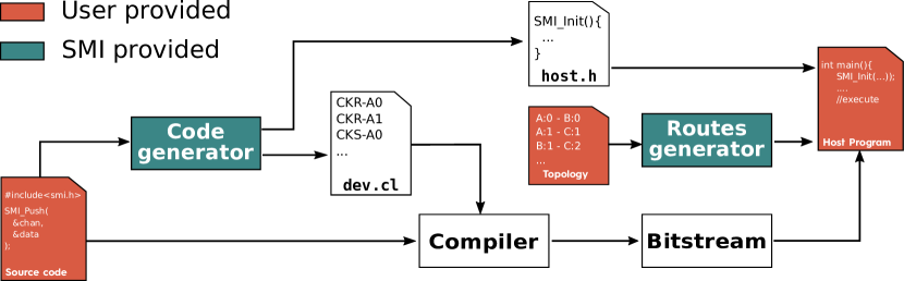
The development workflow for using SMI is depicted on Fig. 10. The communication logic of SMI is produced by a code generator. It takes the description of SMI operations (ports, data types) as an input and outputs a device source file with all the necessary CKS, CKR, communication primitives and collective support kernel implementations that are tailored for the specified set of SMI operations. The code generator also outputs a host header file that contains support functions for SMI initialization.
To generate the correct input to the code generator, we provide a metadata extractor, that parses the user’s device code with Clang, finds all used SMI operations and extracts their metadata to a file. After the code generator is executed on this metadata, the code-generated SMI implementation can be compiled together with the the user’s code by an FPGA compiler to produce a bitstream. For SPMD programs, only one instance of the code is generated, and thus the user only needs to build a single bitstream for any number of nodes in a multi-FPGA system.
A route generator accepts the network topology of the FPGA cluster and produces the necessary routing tables that drive the forwarding logic at runtime. The topology is provided as a JSON file, which describes connections between FPGA network ports. The route generator needs to access metadata created by the code generator, but it doesn’t modify or create any source code and therefore it can be executed independently from the compilation (crucially, you can change the routes without recompiling the bitstream).
Finally, the user host program takes the compiled bitstream and the routing tables as inputs, and uses functions provided by the generated host header to setup the routing tables, and to start all of the SMI transport components on the FPGA. We also provide build system integration for CMake which fully automates the full workflow with a single function invocation.
4.6. Implementation Portability
The proof-of-concept implementation of SMI discussed here targets the Intel FPGA SDK for OpenCL, but as SMI is a platform independent interface specification, it can be implemented for other vendors, such as Xilinx FPGAs, as well. The interface, and key concepts of the transport component can be reused, adapting it to the target platform and SDK (changing the pragma style, FIFO buffer management, etc.). However, the current implementation exploits Intel OpenCL I/O channels to perform communications using the on-board network interfaces. To the best of our knowledge, other vendors do not expose similar high level network interfaces directly from the shell to the HLS programmer. Therefore, additional IP cores would be necessary to port the transport component.
5. Evaluation
To analyze the expressiveness of SMI and the performance of our reference implementation, we implement four microbenchmarks and two distributed applications, showing both the SPMD and MPMD approaches of writing SMI-based kernels.
5.1. Experimental Setup
We target the Noctua cluster at the University of Paderborn, which contains Nallatech 520N boards, each carrying a Stratix 10 GX2800 FPGA chip. The board exposes 4 quad small form-factor pluggable (QSFP) transceivers as network ports, each rated at . The QSFP interfaces do not implement a full reliable network stack, but implement error correction, flow control, and handle backpressure, which we can rely on in our communication layer. We target the 18.1.1_max BSP provided by Nallatech, which exposes the QSFP ports as 8 I/O channels (4 input and 4 output) per device. The I/O channels exposed to HLS are 256 bit wide, and can be accessed using read/write primitives. All hardware kernels (applications and transport layer) running on the device is implemented in OpenCL, and are compiled with the Intel Quartus Prime Pro 18.1.1 toolset.
Within the target cluster, each node contains two FPGA devices, and the QSFP ports of different FPGAs are directly connected to each other (either within or between nodes). The FPGA interconnection topology is described by a list of point-to-point connections, which is used to generate the routing tables. For the experiments performed here, we had access to 8 FPGAs connected in a 2D torus, such that all the 4 QSFP ports in each FPGA are wired to 4 distinct other FPGAs. Each host node is equipped with two Intel Xeon Gold 6148F CPUs, for a total of 40 cores operating at , and have of DRAM. The nodes are interconnected using an Intel Omni-Path network. Host code is compiled using gcc v7.3 and OpenMPI v3.1.
All experiments were executed multiple times until 99% confidence interval is within 5% of the measured median. For the tests in which there is no host intervention, few runs were sufficient to meet this condition, due to the highly deterministic nature of FPGA codes. Then, median times have been considered for producing the reported performance figures.
5.2. FPGA Resource Utilization
Tab. 1 shows the FPGA resource consumption of SMI, in terms of lookup tables (LUTs), flip-flops (FFs) and on-chip memory blocks (M20Ks). The table reports resources consumed by the interconnection structure (Interconn.) and communication kernels (C.K.) both in absolute values and in fractions of the total resource capacity. We consider two scenarios: one where only a single network port is used, and one where all the four available network ports are utilized. In the former case, only one pair of communication kernels is deployed. In the latter, 4 CKS/CKR kernels are used, leading to additional interconnect logic. In either case, we consider one application endpoint attached per CKS/CKR pair.
| 1 QSFP | 4 QSFPs | |||||
|---|---|---|---|---|---|---|
| LUTs | FFs | M20Ks | LUTs | FFs | M20Ks | |
| Interconn. | 144 | 4,872 | 0 | 1,152 | 39,264 | 0 |
| C. K. | 6,186 | 7,189 | 10 | 30,960 | 31,072 | 40 |
| % of max | 0.3% | 0.7% | 0% | 1.7% | 1.9% | 0.3% |
The the number of used resources grows slightly faster than linear. This is due to the fact that the number of input/output channels that the communication kernels must handle increases with the number of used QSFPs. In all cases, the resource overhead of SMI is insignificant, amounting to less than of the total chip resources. Tab. 2 reports the resource consumption of the support kernels used to implement the collectives evaluated in the following. These numbers are for 32-bit floating point data, and with SUM as the Reduce operation.
| LUTs | FFs | M20Ks | DSPs | |
|---|---|---|---|---|
| Broadcast | 2,560 (0.1%) | 3,593 (0.1%) | 0 (0%) | 0 (0%) |
| Reduce (FP32 SUM) | 10,268 (0.6%) | 14,648 (0.4%) | 0 (0%) | 6 (0.1%) |
5.3. Microbenchmarks
To measure how well our reference implementation can exploit the experimental setup, we evaluate its key characteristics by using a set of four microbenchmarks. Communication kernels use , and an eager transmission protocol is used for point-to-point communication.
5.3.1. Bandwidth
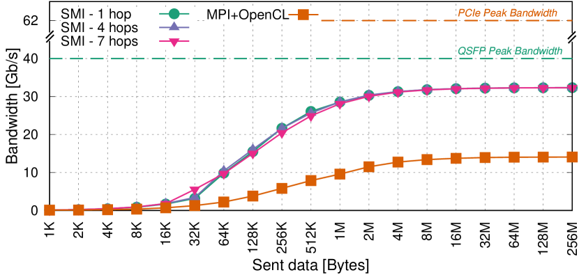
In this benchmark, a source application streams a large message to a receiver. To test our routing approach, and measure the properties of SMI on less connected topologies, we vary our connection topology so that the two applications are at different network distances (hops), by disabling other connections as needed. This is done by changing the connection list used to compute the routes, so that the 8 FPGAs are treated as being organized along a linear bus, rather than in a torus (without rebuilding the bitstream).
As a reference comparison for the SMI bandwidth, we consider a data transfer performed through the host stack, where the application writes the message into off-chip DRAM on the device, transfers it across PCIe to the host, sends it to the remote host using an MPI_Send primitive. On the receiving host, symmetric operations are performed. Fig. 11 shows the achieved bandwidth by varying the message size and considering only the payload as data exchanged. SMI approaches of the peak bandwidth offered by the QSFP connection, which is when taking the header of each network into account. Because the message is streamed, larger network distance (in the absence of contention in the network) does not affect the achieved bandwidth. Despite using a higher bandwidth interconnect, the host-based implementation achieves approximately one third of the SMI bandwidth, due to the long sequence of copies through local device memory, local PCIe, host network, remote PCIe, and remote device memory.
While this benchmark shows the bandwidth advantage on the tested PCIe-attached setup, SMI is not coupled to a specific transport layer. For example, in FPGAs with a high bandwidth cache-coherency bus to the host CPU (e.g., Intel HARP devices), or where a NIC can write to FPGA memory directly, it could be more beneficial to use the general purpose interconnect as the transport backend instead.
5.3.2. Latency
We measure the message latency by implementing a ping-pong benchmark of a small message between two ranks, and measure the latency as half the execution time of a single round-trip. Tab. 3 shows the measured latency. As comparison reference we implemented the same benchmark by using host based communications. As expected, SMI is able to obtain a much lower latency, and the time needed to reach the target increases linearly with the increase of the network distance.
| MPI+OpenCL | SMI-1 | SMI-4 | SMI-7 |
| 36.61 | 0.801 | 2.896 | 5.103 |
5.3.3. Injection rate
We measure the number of cycles that pass before a CKS (or CKR) is able to inject another request from the same application endpoint: i.e., the injection latency of the design. The injection rate is computed from this according to the clock frequency of the design. To benchmark this, we use a sender application that opens a send channel and sends a message with one element at every iteration of a pipelined loop (i.e., every clock cycle). Independent of the network, the sender is thus capable of an injection rate equivalent to the clock frequency of the design.
We benchmark the scenario in which we have 4 communication channels per FPGA with 4 CKR/CKS pairs and we let the parameter vary. We measure the injection rate by dividing the number of injected messages by the kernel execution time, then multiplying this by the clock frequency to obtain the injection latency.
| 5 | 2.5 | 1.8 | 1.69 |
|---|
For the case in which we measure clock cycles. This latency is due to the implemented packet switching protocol (see Sec. 4.3), where the CKS module polls a different port at every cycle, corresponding to a latency of 5 cycles (1 from the application, 1 from CKR, 3 from other CKS modules). As long as increases, the injection rate decreases as the communication kernels will spend more time in reading from the same port.
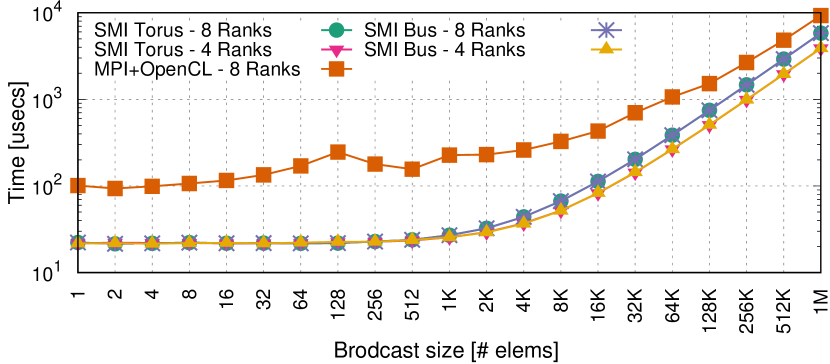
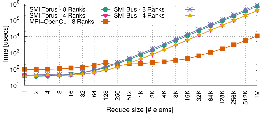
5.3.4. Collective operations
We benchmark the time required to broadcast and reduce a message of varying size between 4 and 8 FPGAs, considering two different connection topologies: a torus, and a linear bus. The evaluation is done with 32-bit floating point data and with SUM as the Reduce operation. Results are shown in Fig. 12 and Fig. 13 for broadcast and reduce, respectively. For broadcast, SMI is able to achieve lower communication time for all the considered input sizes. SMI achieves similar performance independently of the considered connection topology. For small to medium-sized messages, SMI’s Reduce outperforms going over the host using OpenCL and MPI, but loses its benefit at high message sizes. The credit-based flow control algorithm implemented by the root is latency sensitive, therefore the time to completion increases with the diameter of the network. The SMI reference implementation does not yet implement tree-based collectives, resulting in a higher congestion in the root rank.
5.4. Applications
5.4.1. GESUMMV
Dense linear algebra makes up some of the most common routines in HPC applications, and are good candidates for exploiting the spatial parallelism offered by FPGAs. We consider the GESUMMV routine, which is a part of the Extended BLAS set (Blackford et al., 2002), which in turn invokes BLAS subroutines. It computes , where and are scalars, and are vectors of length , and and are matrices of size . To show the benefit of SMI, we implement a single chip and a distributed version of the routine. The single-FPGA implementation consists of two matrix-vector multiplications (GEMV routines) that compute in parallel, and stream their results to a vector addition module (AXPY routine) producing the final result (Fig. 14, left). As these routines are memory-bound, the computation is bottlenecked by memory bandwidth.
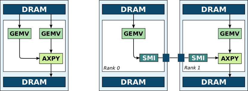
The distributed implementation is obtained by functional decomposition, and it is implemented as a MPMD program using two ranks (Fig. 14, right). Rank 0 computes the first matrix-vector multiplication and sends the result elements to rank 1 using an SMI channel. On rank 1, the second matrix-vector multiplication and the vector addition are performed, receiving data from both local DRAM and the remote GEMV routine. The full application thus gains access to twice the memory bandwidth across the two FPGAs. The implementations of GEMV and AXPY are derived from an open-source synthesizable library (Matteis et al., 2019).
Fig. 15 shows the expected speedup of of the distributed implementation over the single-chip implementation. Execution times of the SMI benchmarks are reported on top of the histogram boxes. Adapting the application required only minimal code modifications to the kernel, with a difference of 8 lines of code: GEMV on rank 0 is changed to perform an SMI send rather than pushing its result to a regular FIFO, and the vector addition is modified to read one of its inputs from an SMI network channel.
5.4.2. Stencil
Stencil applications are a suitable target for FPGA acceleration, as their regular access pattern allows implementing memory reuse schemes that make highly efficient use of on-chip memory. Even with perfect reuse across the spatial domain, however, stencils generally exhibit low computational intensity. Additional reuse can be obtained by using time tiling, which is implemented on FPGAs by connecting a linear array of processing elements in a deep pipeline, executing multiple timesteps in parallel (Sano et al., 2014; Zohouri et al., 2018). When parallelizing to multiple FPGAs, Sano et al. (Sano et al., 2014) simply extend this array to multiple FPGAs by using serial connections between them in a streaming model (as conceptually illustrated in Fig. 4).
For large stencil domains, FPGA designs must tile the spatial domain in addition to the time domain, as the required buffer size grows with the size of the domain. This results in a halo region of redundant computations, which is proportional to the number of pipelined timesteps executed in parallel (Zohouri et al., 2018). This puts a hard limit on the scalability of this approach, as the number of redundant computations will in the extreme case dominate “useful” computations. Furthermore, not all stencils require or allow time tiling, leaving spatial parallelism (e.g., vectorization) as the only option to speed up the computation, in which case the problem becomes memory bound. It is thus desirable to parallelize spatially across multiple FPGAs, exploiting both compute resources and memory bandwidth of multiple devices.
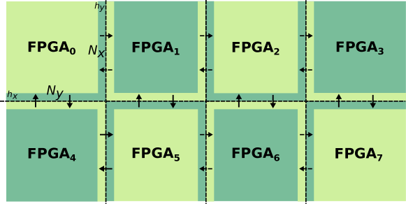
We implement a SPMD distributed memory FPGA stencil code using SMI. The spatial domain is scattered to multiple devices before execution, and the devices exchange halo regions during computation. Shift registers are used to achieve perfect spatial reuse within each FPGA. We decompose the domain in two dimensions, such that each FPGA communicates to and from a north, west, east, and south neighbor, shown in Fig. 16. Additional tiling can be employed for large domains and 3D stencils by further decomposing the domain on each rank without affecting the communication pattern. The communication is naturally expressed with streaming messages in the pipelined code. A snippet of the communication code is shown in Lst. 17: at each timestep, channels are opened to adjacent ranks using a distinct port for each neighbor, and data is read from the network during computation using SMI_Pop commands. Although the west and east halos are not contiguous in memory, they are expressed as a single message in the streaming messages model. Due to the transient nature of SMI channels, all ranks will be configured with the same bitstream, and the rank of adjacent neighbors is computed at runtime. If no neighbor exists (e.g., the west and north neighbor for in Fig. 16), the given channel simply remains unused.
To fully hide communication, the communication volume of the non-halo region of size must be greater than the communication volume of the halo regions of size (send and receive), weighted by the memory bandwidth consumed to read values from memory on each FPGA () and the network bandwidth between two adjacent FPGAs (), respectively (for our system, we consider constant. In larger networks, depends on how ranks are mapped to the network topology). That is, the following inequality must hold:
Since the left-hand side grows quadratically with the stencil domain size, this condition is easily met when tackling large problems.
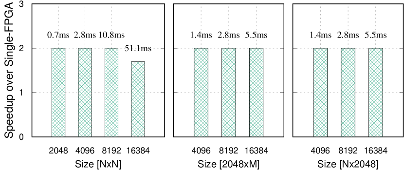
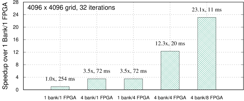
For benchmarks we use a 4-point stencil (i.e., ). We demonstrate the benefit of spatial tiling in a distributed memory FPGA setting using SMI by showing the strong scaling behavior of five kernels executed over the same stencil domain: a vectorized kernel with perfect spatial reuse, reading elements per cycle from a single DDR bank (1 bank/1 FPGA); a spatially tiled kernel running on a single node, reading elements per cycle across all four memory modules of the FPGA (4 banks/1 FPGA); an SMI code running on four FPGAs, each reading elements per cycle from a single memory bank per FPGA (1 bank/4 FPGAs); an SMI code running on four FPGAs, each reading elements per cycle across all memory banks (4 banks/4 FPGAs); and an SMI implementation running on 8 FPGAs organized in a shape, each reading elements per cycle across all memory banks (4 banks/8 FPGAs). Results are shown in Fig. 18 for a domain, executed for 32 timesteps using the torus connection topology. We executed the same benchmarks with the FPGAs organized in a bus topology, and observed this to not affect the execution time.
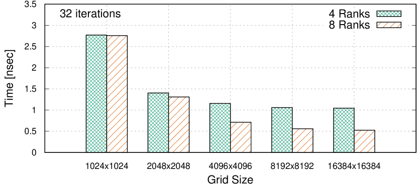
Exploiting four banks on a single FPGA, and exploiting one bank per FPGA on four FPGAs, both show a nearly identical speedup of , demonstrating that communication and computation is fully overlapped. When reading elements on four FPGAs, we get the exact product as speedup over the single bank version, while 8 FPGAs exhibit a speed of . In Fig. 19 we evaluate weak scaling, by reporting the average computation time per grid point obtained with different grid sizes for the 4 and 8 FPGAs setups. At large grid sizes, 8 FPGAs achieve a 2x speedup over 4 FPGAs.
With SMI and our reference implementation, we show that we can execute FPGA programs in both MPMD and SPMD fashion, target any network topology, specialize to the target network topology, and scale the number of FPGAs using the same bitstream. Adapting to SMI requires minimal code intervention, as the interface integrates into the conventional streaming approach taken by pipelined HLS codes, and is thus nearly equivalent to parallelizing the code on a single device.
6. Related Work
In previous work targeting multi-FPGA systems, FPGAs interconnected by point-to-point serial connections are typically programmed according to the streaming model (Fig. 4). The common approach to scaling to multiple FPGAs is to organize the computation in a pipeline spanning across multiple chips, in which each stage communicates only with the previous and the successive stage (e.g., systolic array approaches). Sato et. al. (Sano et al., 2014) parallelize 2D and 3D stencils in this way by pipelining a linear array of processing elements across multiple FPGAs. Each processing element performs one time-step, and the results are streamed to the next one. Zhang et al. (Zhang et al., 2016) propose an implementation of a convolutional neural network that pipelines 6 FPGA devices connected in a ring topology. In their solution, a network layer is implemented by a single stage. Geng et al. (Geng et al., 2018) addresses a similar problem by proposing a pipelined implementation in which layers are distributed across multiple pipeline stages. Owaida et al. (Owaida and Alonso, 2018) parallelize the inference over a decision tree ensemble. They proposed a communication shell to implement communications between FPGAs either by using serial links or via host intervention. In all the aforementioned cases, the application programmer is limited to the streaming model in expressing a distributed computation, constructing the exact path to move the data across the FPGAs in the system. With streaming messages and SMI we propose a more flexible solution, allowing programmers to dynamically exploit arbitrary communication topologies in the spirit of MPI, while maintaining a streaming programming model for computations.
Despite accelerators being ubiquitous in supercomputers and data centers, there is no unified programming model or library for communicating directly from/to accelerator devices. Traditionally, programmers have been forced to use a mix of different programming models (e.g, MPI+CUDA or MPI+OpenCL). More recently, there has been an effort from the HPC community in developing programming models and libraries that treat accelerators as first-class citizens: Aji et al. (Aji et al., 2016) propose MPI-ACC, an accelerator-aware MPI implementation, to support data transfers in heterogeneous clusters; Gysi et al. (Gysi et al., 2016) propose dCuda, which combines the CUDA programming model with a subset of MPI remote memory access operations; and the authors of IMPACC (Kim et al., 2016) propose integrating MPI and OpenACC, by mapping all the available host and device memories in a node to a single unified node virtual address space. All these solutions involve intervention of the host to perform the actual data communication. In SMI, we provide an accelerator-oriented communication library, and show how this can be used to exploit a dedicated FPGA interconnect, avoiding costly trips through the host nodes, saving PCIe, host DRAM, and host network bandwidth.
In the context of FPGA programming, various works address applying the message passing model to multi-FPGA systems. TMD-MPI (Saldaña et al., 2010) implements a subset of MPI primitives for multi-FPGA systems. The authors implement a VHDL-based engine that performs communications, exploiting shared memory (if the FPGAs are attached to the same host) or a specialized network interface (for remote communications). Shu et al. (Shu et al., 2019) propose DUA, a communication architecture that provides uniform access for FPGAs to data center resources like CPUs, GPUs, and disks. The system is implemented in Verilog, but provides an OpenCL interface, and targets FPGAs implementing a full network stack in a cloud setting. The system provides basic message-passing primitives, but does not go further to address the programming model. Eskandari et al. (Eskandari et al., 2019) propose HUMboldt, a message passing communication layer, supporting messages to be sent among different FPGA kernels and CPU kernels. In all these works, authors apply the message passing model directly to program a multi-FPGA system. With SMI, we explicitly address the issue of programming communication in a pipelined HLS setting, providing a model and interface that is familiar to HPC users, yet integrates well into hardware designs.
Finally, George et al. (George et al., 2016) present a network infrastructure for allowing communication among FPGAs organized in a 3D torus. In their subsequent work (Lawande et al., 2016), they build an OpenCL abstraction on top of this network stack to enable inter-FPGA communications in HLS programs. In contrast to SMI, their solution exploits the streaming model, without defining a precise communication interface and with no support for collective communications.
7. Conclusion
We propose streaming messages, a communication model for distributed memory programming on reconfigurable hardware. Streaming messages unify message passing and traditional streaming communication, allowing transient channels to be dynamically established between multiple FPGAs in distributed systems, while maintaining a programming model that integrates seamlessly into HLS designs. To capture and expose the semantics of streaming messages, we introduce SMI, a communication interface specification for HLS programs, drawing inspiration from MPI, but designed to fit the hardware programming model, and release an open source reference implementation for use with OpenCL-capable Intel FPGAs. With the simple and powerful model offered by SMI, we hope to further the viability of FPGAs as a HPC accelerators, and make distributed programming on FPGAs more accessible to both HPC and hardware developers.
Acknowledgements.
We wish to thank the Paderborn Center for Parallel Computing (PC2), in particular Christian Plessl and Tobias Kenter, for access, support, maintenance, and upgrades, sometimes on very short notice. We also would like to thank Mohamed Issa (Intel Corporation), for valuable suggestions. This project has been supported from the European Research Council (ERC) under the European Union’s Horizon 2020 programme, Grant Agreement No. 678880 (DAPP), and Grant Agreement No. 801039 (EPiGRAM-HS). Jakub Beránek was supported by the European Science Foundation through the “Science without borders” project, reg. nr. CZ.02.2.69/0.0./0.0./16_027/ 0008463 within the Operational Programme Research, Development and Education.References
- (1)
- Aji et al. (2016) A. M. Aji, L. S. Panwar, F. Ji, K. Murthy, M. Chabbi, P. Balaji, K. R. Bisset, J. Dinan, W. Feng, J. Mellor-Crummey, X. Ma, and R. Thakur. 2016. MPI-ACC: Accelerator-Aware MPI for Scientific Applications. IEEE Transactions on Parallel and Distributed Systems 27, 5 (May 2016), 1401–1414. https://doi.org/10.1109/TPDS.2015.2446479
- Blackford et al. (2002) Susan Blackford, James Demmel, Jack Dongarra, Iain Duff, Sven Hammarling, Greg Henry, Michael Heroux, Linda Kaufman, Andrew Lumsdaine, Antoine Petitet, Roldan Pozo, Karin Remington, and Clint Whaley. 2002. An Updated Set of Basic Linear Algebra Subprograms (BLAS). ACM Trans. Math. Softw. 28, 2 (June 2002), 135–151.
- Chung et al. (2018) E. Chung, J. Fowers, K. Ovtcharov, M. Papamichael, A. Caulfield, T. Massengill, M. Liu, D. Lo, S. Alkalay, M. Haselman, M. Abeydeera, L. Adams, H. Angepat, C. Boehn, D. Chiou, O. Firestein, A. Forin, K. S. Gatlin, M. Ghandi, S. Heil, K. Holohan, A. El Husseini, T. Juhasz, K. Kagi, R. Kovvuri, S. Lanka, F. van Megen, D. Mukhortov, P. Patel, B. Perez, A. Rapsang, S. Reinhardt, B. Rouhani, A. Sapek, R. Seera, S. Shekar, B. Sridharan, G. Weisz, L. Woods, P. Yi Xiao, D. Zhang, R. Zhao, and D. Burger. 2018. Serving DNNs in Real Time at Datacenter Scale with Project Brainwave. IEEE Micro 38, 2 (Mar 2018), 8–20. https://doi.org/10.1109/MM.2018.022071131
- Cong et al. (2011) J. Cong, B. Liu, S. Neuendorffer, J. Noguera, K. Vissers, and Z. Zhang. 2011. High-Level Synthesis for FPGAs: From Prototyping to Deployment. IEEE Transactions on Computer-Aided Design of Integrated Circuits and Systems 30, 4 (April 2011), 473–491. https://doi.org/10.1109/TCAD.2011.2110592
- Czajkowski et al. (2012) Tomasz S Czajkowski, Utku Aydonat, Dmitry Denisenko, John Freeman, Michael Kinsner, David Neto, Jason Wong, Peter Yiannacouras, and Deshanand P Singh. 2012. From OpenCL to high-performance hardware on FPGAs. In 22nd international conference on field programmable logic and applications (FPL). IEEE, 531–534.
- de Fine Licht et al. (2018) Johannes de Fine Licht, Simon Meierhans, and Torsten Hoefler. 2018. Transformations of High-Level Synthesis Codes for High-Performance Computing. CoRR abs/1805.08288 (2018). arXiv:1805.08288 http://arxiv.org/abs/1805.08288
- Dimond et al. (2011) Rob Dimond, Sébastien Racaniere, and Oliver Pell. 2011. Accelerating large-scale HPC Applications using FPGAs. In 2011 IEEE 20th Symposium on Computer Arithmetic. IEEE, 191–192.
- Domke et al. (2011) J. Domke, T. Hoefler, and W. E. Nagel. 2011. Deadlock-Free Oblivious Routing for Arbitrary Topologies. In 2011 IEEE International Parallel Distributed Processing Symposium. 616–627. https://doi.org/10.1109/IPDPS.2011.65
- Eskandari et al. (2019) Nariman Eskandari, Naif Tarafdar, Daniel Ly-Ma, and Paul Chow. 2019. A Modular Heterogeneous Stack for Deploying FPGAs and CPUs in the Data Center. In Proceedings of the 2019 ACM/SIGDA International Symposium on Field-Programmable Gate Arrays (FPGA ’19). ACM, New York, NY, USA, 262–271. https://doi.org/10.1145/3289602.3293909
- Geng et al. (2018) T. Geng, T. Wang, A. Sanaullah, C. Yang, R. Xu, R. Patel, and M. Herbordt. 2018. FPDeep: Acceleration and Load Balancing of CNN Training on FPGA Clusters. In 2018 IEEE 26th Annual International Symposium on Field-Programmable Custom Computing Machines (FCCM). 81–84.
- George et al. (2016) A. D. George, M. C. Herbordt, H. Lam, A. G. Lawande, J. Sheng, and C. Yang. 2016. Novo-G#: Large-scale reconfigurable computing with direct and programmable interconnects. In 2016 IEEE High Performance Extreme Computing Conference (HPEC). 1–7.
- Gysi et al. (2016) T. Gysi, J. Bär, and T. Hoefler. 2016. dCUDA: Hardware Supported Overlap of Computation and Communication. In SC ’16: Proceedings of the International Conference for High Performance Computing, Networking, Storage and Analysis. 609–620. https://doi.org/10.1109/SC.2016.51
- instances ([n. d.]) Amazon EC2 F1 instances. [n. d.]. https://aws.amazon.com/ec2/instance-types/f1/.
- Kara et al. (2017) Kaan Kara, Dan Alistarh, Gustavo Alonso, Onur Mutlu, and Ce Zhang. 2017. FPGA-accelerated dense linear machine learning: A precision-convergence trade-off. In 2017 IEEE 25th Annual International Symposium on Field-Programmable Custom Computing Machines (FCCM). IEEE, 160–167.
- Kim et al. (2016) Jungwon Kim, Seyong Lee, and Jeffrey S. Vetter. 2016. IMPACC: A Tightly Integrated MPI+OpenACC Framework Exploiting Shared Memory Parallelism. In Proceedings of the 25th ACM International Symposium on High-Performance Parallel and Distributed Computing (HPDC ’16). ACM, New York, NY, USA, 189–201. https://doi.org/10.1145/2907294.2907302
- Kobayashi et al. (2018) Ryohei Kobayashi, Yuma Oobata, Norihisa Fujita, Yoshiki Yamaguchi, and Taisuke Boku. 2018. OpenCL-ready High Speed FPGA Network for Reconfigurable High Performance Computing. In Proceedings of the International Conference on High Performance Computing in Asia-Pacific Region (HPC Asia 2018). ACM, New York, NY, USA, 192–201. https://doi.org/10.1145/3149457.3149479
- Lawande et al. (2016) A. Lawande, A. D. George, and H. Lam. 2016. An OpenCL Framework for Distributed Apps on a Multidimensional Network of FPGAs. In 2016 6th Workshop on Irregular Applications: Architecture and Algorithms (IA3). 42–49. https://doi.org/10.1109/IA3.2016.012
- Matteis et al. (2019) Tiziano De Matteis, Johannes de Fine Licht, and Torsten Hoefler. 2019. FBLAS: Streaming Linear Algebra on FPGA. CoRR (Aug. 2019).
- Message Passing Interface Forum (2015) Message Passing Interface Forum. 2015. MPI: A Message-Passing Interface Standard, Version 3.1. Specification. https://www.mpi-forum.org/docs/mpi-3.1/mpi31-report.pdf
- Owaida and Alonso (2018) M. Owaida and G. Alonso. 2018. Application Partitioning on FPGA Clusters: Inference over Decision Tree Ensembles. In 2018 28th International Conference on Field Programmable Logic and Applications (FPL). 295–2955. https://doi.org/10.1109/FPL.2018.00057
- Saldaña et al. (2010) Manuel Saldaña, Arun Patel, Christopher Madill, Daniel Nunes, Danyao Wang, Paul Chow, Ralph Wittig, Henry Styles, and Andrew Putnam. 2010. MPI As a Programming Model for High-Performance Reconfigurable Computers. ACM Trans. Reconfigurable Technol. Syst. 3, 4, Article 22 (Nov. 2010), 29 pages. https://doi.org/10.1145/1862648.1862652
- Sano et al. (2014) Kentaro Sano, Yoshiaki Hatsuda, and Satoru Yamamoto. 2014. Multi-FPGA accelerator for scalable stencil computation with constant memory bandwidth. IEEE Transactions on Parallel and Distributed Systems 25, 3 (2014), 695–705.
- Shu et al. (2019) Ran Shu, Peng Cheng, Guo Chen, Zhiyuan Guo, Lei Qu, Yongqiang Xiong, Derek Chiou, and Thomas Moscibroda. 2019. Direct Universal Access: Making Data Center Resources Available to FPGA. In 16th USENIX Symposium on Networked Systems Design and Implementation (NSDI 19). USENIX Association, Boston, MA, 127–140. https://www.usenix.org/conference/nsdi19/presentation/shu
- Table ([n. d.]a) Stratix 10 GX/SX Product Table. [n. d.]a. https://www.intel.com/content/dam/www/programmable/us/en/pdfs/literature/pt/stratix-10-product-table.pdf.
- Table ([n. d.]b) Versal ACAP AI Core Series Product Table. [n. d.]b. https://www.xilinx.com/support/documentation/selection-guides/versal-ai-core-product-selection-guide.pdf.
- Umuroglu et al. (2017) Yaman Umuroglu, Nicholas J. Fraser, Giulio Gambardella, Michaela Blott, Philip Leong, Magnus Jahre, and Kees Vissers. 2017. FINN: A Framework for Fast, Scalable Binarized Neural Network Inference. In Proceedings of the 2017 ACM/SIGDA International Symposium on Field-Programmable Gate Arrays (FPGA ’17). ACM, New York, NY, USA, 65–74. https://doi.org/10.1145/3020078.3021744
- Zhang et al. (2016) Chen Zhang, Di Wu, Jiayu Sun, Guangyu Sun, Guojie Luo, and Jason Cong. 2016. Energy-Efficient CNN Implementation on a Deeply Pipelined FPGA Cluster. In Proceedings of the 2016 International Symposium on Low Power Electronics and Design (ISLPED ’16). ACM, New York, NY, USA, 326–331. https://doi.org/10.1145/2934583.2934644
- Zohouri et al. (2018) Hamid Reza Zohouri, Artur Podobas, and Satoshi Matsuoka. 2018. Combined spatial and temporal blocking for high-performance stencil computation on FPGAs using OpenCL. In Proceedings of the 2018 ACM/SIGDA International Symposium on Field-Programmable Gate Arrays. ACM, 153–162.