Observation of stimulated Brillouin scattering in silicon nitride integrated waveguides
Abstract
Silicon nitride (Si3N4) has emerged as a promising material for integrated nonlinear photonics and has been used for broadband soliton microcombs and low-pulse-energy supercontinuum generation. Therefore understanding all nonlinear optical properties of Si3N4 is important. So far, only stimulated Brillouin scattering (SBS) has not been reported. Here we observe, for the first time, backward SBS in fully cladded Si3N4 waveguides. The Brillouin gain spectrum exhibits an unusual multi-peak structure resulting from hybridization with high-overtone bulk acoustic resonances (HBARs) of the silica cladding. The reported intrinsic Brillouin gain at 25 GHz is estimated as m/W. Moreover, the magnitude of the photoelastic constant is estimated as . Since SBS imposes an optical power limitation for waveguides, our results explain the capability of Si3N4 to handle high optical power, central for integrated nonlinear photonics.
Introduction - Integrated photonics has significantly advanced over the past decades. Today, integrated photonics is used to build on-chip lasers which can be found in data centers, and passive optical elements such as filters and arrayed waveguide gratings for optical signal processing. Although silicon and indium phosphide are the most mature platforms, there has been growing interest and advances in silicon nitride (). Amorphous [1] shows exceptional performance in terms of low linear optical losses below 1 dB/m and absence of two-photon absorption, and has been widely used for passive elements such as delay lines and multi-mode interferometers [2]. In addition, the high Kerr nonlinearity and flexibility to engineer the anomalous group velocity dispersion (GVD) via geometry variation [3] have made an ideal platform for integrated nonlinear photonics. Moreover, is suitable for applications in space [4]. Although already considered in the 1980’s for its promise in integrated photonics [5], only recent advancements in nanofabrication for film growth and patterning have overcome the highly tensile film stress of stoichiometric [6, 7]. These developments allow high-yield fabrication of waveguides with tight optical confinement and anomalous GVD, as required for parametric frequency conversion via Kerr nonlinearity [8]. Such integrated waveguides are presently a leading platform for dissipative-Kerr-soliton-based frequency comb ("soliton microcomb") generation [9]. Integrated Si3N4-based soliton microcomb can now operate with ultralow electrical driving power [10, 11] and repetition rate extending down into the microwave domain (e.g. X- and K-band) [12], and have been used for system-level demonstrations [9]. In addition, waveguides enables coherent and low-pulse-energy supercontinuum generation in near-infrared [13], as well as in mid-infrared for dual-comb spectroscopy [14]. Other nonlinear phenomena in waveguides such as second- and third-harmonic generation [15, 16], as well as stimulated Raman scattering (SRS) [17] have been studied. However to date, there is no report on backward Brillouin scattering in . Understanding the acousto-optic interaction in waveguides is key to characterize Brillouin gain, and equally important, to model the noise properties resulting from thermally-excited guided acoustic waves.
Stimulated Brillouin scattering (SBS) is a nonlinear process mediated by acousto-optic interaction inside a medium [18, 19, 20]. It has been observed in various platforms, including silica fibers [21, 22, 23, 24, 25], whispering-gallery-mode resonators [26, 27, 28, 29], and integrated waveguides based on chalcogenide [30, 31], silicon [32, 33] and aluminum nitride [34]. SBS has led to several applications, such as slow and fast light [35, 36], microwave photonic filters [32, 37], microwave synthesis [38], highly coherent laser sources [39, 40], gyroscopes [41, 40], isolators [42], mode-locked lasers [23, 43] and sensors [44]. At the same time, Brillouin scattering poses a power limitation in waveguides and fibers [45], and in addition induces noises via thermal excitation of guided acoustic waves.
Recently, integrated Si3N4 waveguides have been used to demonstrate a Brillouin laser [40]. However in that work, Si3N4 was used solely to guide the light, and the SBS interaction occurred within the silica (SiO2) cladding, as confirmed by the Brillouin frequency shift of 10.9 GHz. A second work proposed the use of Si3N4 membrane including a waveguide and a phononic crystal to explore forward SBS [46, 47]. A third work demonstrated a large light-sound interaction using forward SBS in integrated silicon waveguides [32], while a membrane was used to guide the transverse phonons. However, to date, no work has shown backward SBS in material. Moreover, to the best of our knowledge, there is no reference to the photoelastic tensor (e.g. and ) in the literature.
In this Letter, we characterize, for the first time, the backward SBS gain spectrum in a 5-mm-long waveguide buried in SiO2. Figure 1(a) shows an artist’s view of SBS in a waveguide buried in SiO2. Two optical fields, pump and probe, spatially overlap and are phase-matched with an acoustic mode, which induce acoustic oscillations through electrostriction and subsequent generation of a moving grating. Reciprocally, acoustic waves scatter light via photoelasticity. The phase-matching condition is given by:
| (1) |
where is the effective refractive index of the optical mode, is the probe wavelength, is the acoustic mode velocity and is the Brillouin frequency shift. In the present case, our waveguide cross-section is a m2 trapezoid, exhibiting a smaller width at the top (see Supplementary Material), as shown in the false-color scanning electron microscopy (SEM) image in Fig. 1(a) inset. The refractive indices of and SiO2 at 1550 nm are and , respectively.
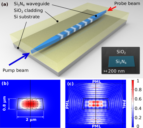
(a) Artist’s view of SBS in a waveguide. Note that the length of the inverse tapers is exaggerated for illustrative purpose. The actual taper length is 300 m, while the full length of the waveguide is 5 mm. White and blue shading represents the material density variation generated by SBS when the pump and probe beams overlay. Inset: false-color SEM of the waveguide cross-section of m2. (b) Normalized electric field distribution for the optical TElike mode. The arrows represent the direction and strength of the electric field in the cross-section plane. (c) Normalized displacement field norm for the fundamental acoustic mode. Visible waves exiting the waveguide indicate a rather high phonon leakage rate. A PML is surrounding the entire domain and absorbs these waves. The vertical black line visible in (b) and (c) is indicative of the waveguide symmetry.
The waveguide fundamental quasi-transverse electric (TElike) mode is adiabatically excited by inverse nanotapers [48, 49] placed at chip facets. The simulated optical mode profile in the waveguide using finite-element method (FEM) is shown in Fig. 1(b). The computed effective refractive index and mode area are and 1.2 m2, respectively. A solid mechanics simulation of the fundamental acoustic mode displacement field norm is shown in Fig. 1(c). The details about the simulations are provided in the Supplementary Material. Due to the weak confinement caused by the lower acoustic velocity in SiO2 and by the small waveguide dimension, acoustic waves propagate away from the waveguide and are absorbed by the surrounding perfectly matched layer (PML) [18, 50]. Moreover, the mode shape in the waveguide substantially deviates from the usual bell shape. This is caused by the small waveguide dimensions inducing hybrid acoustic modes [51]. Due to the negligible optical evanescent field in SiO2 cladding, SBS happens mainly in . Indeed, our simulations show that the SiO2 contributes to of the total Brillouin gain of the aforementioned acoustic mode.
Experiments and results - Residual reflections between the two chip facets make the waveguide a low-finesse Fabry-Pérot (FP) cavity. The transmission spectrum of the waveguide is shown in Fig. 2(a), exhibiting a FP cavity free spectral range (FSR) of GHz, corresponding to the 5-mm waveguide length. This cavity causes several experimental challenges: (1) The probe transmission is intensity-modulated by low-frequency random environmental fluctuations (e.g. temperature changes due to variations in the coupling ratio of the pump beam), which constantly shifts the FP cavity’s transmission spectrum. In our experiments, this process generates a noise of standard deviation times higher than the Brillouin signal. (2) Intensity modulation of the pump signal modulates the cavity refractive index via Kerr effect. The resulting time-dependent shift of the FP cavity transmission spectrum modulates the probe signal. Hence, pump intensity variations are transferred to the probe signal and generate a noisy background of standard deviation two times larger than the Brillouin peak gain. (3) In our work, the chip is coupled via two 1-m-long standard single-mode fiber patchcords [52] in which the pump and probe counter-propagate and, as a result, SRS occurs along those fibers and generates a noisy background signal. This process contributes to a lesser extent to the system noise ( 10% of the Brillouin peak gain). Note that SRS is considered much smaller than for silica [17] and can be neglected. Details about the estimates given above are provided in the Supplementary Material.
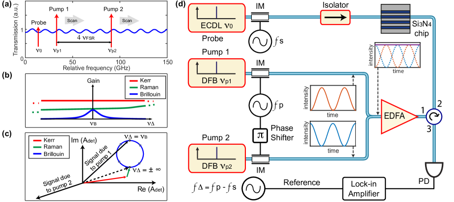
To overcome the three aforementioned challenges, we developed a novel technique, triple intensity modulation (TIM), able to measure the exact Brillouin gain profile. This technique is now explained in details. The pump and probe beams are intensity-modulated at frequency and respectively, and the detection is made at the frequency difference (in our experiment, 20 MHz and = 75 kHz). This implementation exploits the nonlinear nature of SBS leading to sum-difference frequency generation, and has two benefits: (1) It moves the signal detection frequency away from the direct-current (DC) frequency, where the low-frequency environmental noises lie. (2) It efficiently filters the pump reflection out from the probe beam in the radio-frequency (RF) domain. The filtering is achieved by detecting the signal at a distant frequency from the modulated pump frequency via a lock-in amplifier, eliminating the need for high extinction optical filtering. Such a technique is commonly used to filter out stray light in Brillouin microscopy [53].
The aforementioned Kerr effect and Raman scattering issues are resolved by cancelling the temporal variation of the pump intensity. A similar method has been developed to cancel the non-resonant background in coherent anti-Stokes Raman spectroscopy [54]. This is realized by adding a second modulated pump beam (i.e. pump 2), whose intensity and polarization match perfectly those of the first pump (i.e. pump 1). The optical frequency of pump 2 () is increased compared to that of pump 1 () by a multiple of the chip FP cavity FSR: , (in our experiment, n = 4), as illustrated in Fig. 2(a). In this way, both pumps’ intensities remain identical at all times inside the chip, irrespective of environmental noises. In addition, the two pumps are intensity-modulated at the same frequency but are -phase shifted, such that perfect intensity cancellation of the modulation frequency occurs. Hence, the Kerr effect no longer modulates the probe transmission, due to the constant total pump intensity. Moreover, the SRS gain experienced by the probe is nearly identical for each pump, because the frequency difference of the two pumps, , is much smaller than the silica Raman gain bandwidth ( 7 THz).
Since the two pumps are modulated with -phase difference, SRS is attenuated at the detection frequency . For SBS, however, the probe only interacts with pump 1. The situation is summarized in Fig. 2(b) in which the gain behaviour of the Kerr effect (phase-to-intensity conversion can be seen as a gain process for the probe beam), SRS and SBS are sketched in function of the pump-probe detuning frequency , where is the probe frequency. It can be seen that Kerr effect is flat over the entire detuning frequency range and the Raman gain of the silica patchcord is nearly flat over the Brillouin gain bandwidth. Thus, these two contributions result in an identical gain for the two pumps. As the pumps have a -phase difference, these effects cancel out at the detection frequency . A different view of this cancellation is represented in Fig. 2(c) where the different contributions of the probe detection signal , are represented in the complex-plane, for the two pumps. Kerr effect and SRS generate a background signal (dotted arrow) that is cancelled by pump 2. The blue circle represents the path of the SBS Lorentzian amplitude lineshape that is traced when the pump-probe detuning frequency , is scanned. Brillouin gain spectral shape is measured by scanning the two pump frequencies and , while fixing the probe frequency . The two pump frequencies are scanned simultaneously such that their frequency difference remains constant during the scanning, as illustrated in Fig. 2(a).
The experimental setup is shown in Fig. 2(d). The two pumps are generated by two distributed feedback (DFB) lasers and the frequency scanning is performed by temperature control of these lasers. In the small gain approximation [55], the magnitude of the measured amplitude in the presence of SBS in the waveguide can be written as [56]:
| (2) |
where is the photodetector power-to-voltage conversion factor, is the time-averaged detected probe power, is the time-averaged pump power in the waveguide (pump 1 only), is the Brillouin peak gain in unit of , is the waveguide length, and is the gain lineshape.
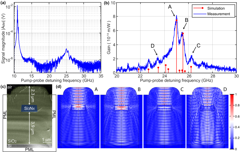
Figure 3(a) shows the magnitude of the measured amplitude , when the pump-probe detuning frequency is scanned from 10 to 35 GHz. The peak to the left is the silica Brillouin gain of the 1-m-long fiber patchcords connecting to the waveguide, and the signal around 25 GHz is the Brillouin gain. Since these two gains are measured jointly, their ratio provides an additional way to estimate the Si3N4 Brillouin gain value. Figure 3(b) shows the measured gain spectrum along with our simulation results. A main peak reaching 10-14 m/W is found at 25 GHz, accompanied by other smaller peaks. The details about error estimation are provided in the Supplementary Material. Using the phase matching condition Eq. 1, the velocity of the main acoustic mode is calculated as 10.5 km/s, which agrees with the literature [58]. The full width at half maximum of the main peak MHz, is obtained by a Lorentzian fitting. Figure 3(d) shows the FEM simulations performed over a 3D trench of the entire chip cross-section including the SiO2-air top interface and SiO2-silicon-substrate bottom interface. The simulation model is built using the precisely measured parameters from SEM as shown in Fig. 3(c). The details about the simulations are provided in the Supplementary Material. Acoustic eigenmodes, computed from 21 to 27 GHz, show that the multiple peaks in the gain spectrum originate from the hybridization with high-overtone bulk acoustic resonances (HBARs) caused by the reflection of acoustic waves at the SiO2-air top boundary and SiO2-silicon-substrate bottom boundary [59].
Discussion - In our waveguide, the optical mode can be approximated as a transverse mode. Then, the Brillouin gain in units m/W, can be expressed as:
| (3) |
where is the refractive index, is the speed of light in vacuum, is the material density, is the photoelastic constant, is the acoustic damping and is the acousto-optic overlap coefficient. We now discuss on the three main parameters: , and .
The acoustic damping is proportional to the Brillouin linewidth as , where represents material damping caused by phonon absorption, and represents phonon leakage from the waveguide. The Brillouin linewidth measured here is 10-times larger than that of silica (), leading to a tenfold gain reduction. Note that, material damping generally follows a square dependence on the Brillouin frequency shift () [60]. Compared to 11 GHz silica Brillouin shift, a fivefold increase in material damping is expected in : . Therefore the remaining damping is assumed to be due to phonon leakage: .
The photoelastic constant quantifies the amount of stress induced in the material by an electric field due to electrostriction. By fitting the peak heights of the FEM simulation results to the measured gain spectrum, the estimated photoelastic constant magnitude , is obtained:
| (4) |
The details about error estimation are provided in the Supplementary Material. This value corresponds to a 5.7-times reduction with respect to that of silica, leading to a 33-times gain decrease as .
The acousto-optic overlap coefficient is the coupling strength between the optical mode and the acoustic mode in relation to their spatial distributions. For example, almost perfect overlap of optical and acoustic modes is achieved in optical fibers, i.e. . Our simulations show an acousto-optic overlap as .
By substituting all these contributions to Eq. 3, we obtain a theoretical 342-times gain reduction in waveguides compared to single-mode fibers. The Brillouin gain value measured in our waveguide, in units m/W, is 250-times smaller than the silica intrinsic gain (), in agreement with the theoretical value derived above. When the intrinsic gain is considered, however, phonon leakage is absent and acousto-optic overlap is unity (). Therefore, the intrinsic Brillouin gain is estimated as , 30-times smaller than that of silica.
In addition, the SBS threshold [61] is estimated as 87 kW (see Supplementary Material). To give two comparisons, a 1-m-long standard single-mode fiber has a SBS threshold of 100 W and a hypothetical silica waveguide with the same dimensions as our waveguide would have a SBS threshold power of 20 kW.
Conclusion - We have characterized backward SBS in integrated waveguides. The observed SBS gain spectrum exhibits multiple peaks due to the hybridization with bulk acoustic resonance modes in the presence of SiO2 cladding of finite thickness. The calculated acoustic velocity in from the measured Brillouin frequency shift (Eq. 1) agrees with the reported value in Ref. [58]. Note that the observed SBS frequency shift in of 25 GHz is the largest SBS frequency value reported on integrated platforms [18]. In addition, the SBS threshold in is estimated as 87 kW in our 5-mm-long waveguide. Since SBS usually limits the maximum optical power in waveguides, its high threshold in shows excellent high power handling capability of central for integrated nonlinear photonics such as soliton microcomb [9] and chip-based supercontinuum generation [13]. Our work also allows assessing the fundamental noise associated with light propagation in Si3N4 waveguides as caused by thermal excitations of acoustic modes.
Acknowledgments: This work was supported by the Swiss National Science Foundation (SNSF) under grant agreement No. 159897, 178895, 176563 (BRIDGE), and by funding from the European Union’s H2020 research and innovation programme under FET Proactive grant agreement No. 732894 (HOT), and by the Defense Advanced Research Projects Agency (DARPA), Microsystems Technology Office (MTO) under contract No. HR0011-15-C-0055 (DODOS). J.H. acknowledges the support provided by Prof. Hwa-Yaw Tam and from the GRF of the Hong Kong Government under project PolyU 152207/15E. The Si3N4 samples were fabricated in the EPFL center of MicroNanoTechnology (CMi).
Data Availability Statement: The code and data used to produce the plots within this work will be released on the repository Zenodo upon publication of this preprint.
References
- Moss et al. [2013] D. J. Moss, R. Morandotti, A. L. Gaeta, and M. Lipson, Nature Photonics 7, 597 (2013).
- Blumenthal et al. [2018] D. J. Blumenthal, R. Heideman, D. Geuzebroek, A. Leinse, and C. Roeloffzen, Proceedings of the IEEE, Proceedings of the IEEE 106, 2209 (2018).
- Foster et al. [2006] M. A. Foster, A. C. Turner, J. E. Sharping, B. S. Schmidt, M. Lipson, and A. L. Gaeta, Nature 441, 960 (2006).
- Brasch et al. [2014] V. Brasch, Q.-F. Chen, S. Schiller, and T. J. Kippenberg, Optics Express 22, 30786 (2014).
- Henry et al. [1987] C. H. Henry, R. F. Kazarinov, H. J. Lee, K. J. Orlowsky, and L. E. Katz, Applied Optics 26, 2621 (1987).
- Luke et al. [2013] K. Luke, A. Dutt, C. B. Poitras, and M. Lipson, Optics Express 21, 22829 (2013).
- Pfeiffer et al. [2018] M. H. P. Pfeiffer, C. Herkommer, J. Liu, T. Morais, M. Zervas, M. Geiselmann, and T. J. Kippenberg, IEEE Journal of Selected Topics in Quantum Electronics 24, 1 (2018).
- Kippenberg et al. [2004] T. J. Kippenberg, S. M. Spillane, and K. J. Vahala, Physical Review Letters 93, 083904 (2004).
- Kippenberg et al. [2018] T. J. Kippenberg, A. L. Gaeta, M. Lipson, and M. L. Gorodetsky, Science 361, eaan8083 (2018).
- Stern et al. [2018] B. Stern, X. Ji, Y. Okawachi, A. L. Gaeta, and M. Lipson, Nature 562, 401 (2018).
- Raja et al. [2019a] A. S. Raja, A. S. Voloshin, H. Guo, S. E. Agafonova, J. Liu, A. S. Gorodnitskiy, M. Karpov, N. G. Pavlov, E. Lucas, R. R. Galiev, A. E. Shitikov, J. D. Jost, M. L. Gorodetsky, and T. J. Kippenberg, Nature Communications 10, 680 (2019a).
- Liu et al. [2019a] J. Liu, E. Lucas, A. S. Raja, J. He, J. Riemensberger, R. N. Wang, M. Karpov, H. Guo, R. Bouchand, and T. J. Kippenberg, arXiv 1901.10372 (2019a).
- Gaeta et al. [2019] A. L. Gaeta, M. Lipson, and T. J. Kippenberg, Nature Photonics 13, 158 (2019).
- Guo et al. [2019] H. Guo, W. Weng, J. Liu, F. Yang, W. Hansel, C. S. Brès, L. Thévenaz, R. Holzwarth, and T. J. Kippenberg, arXiv 1908.00871 (2019).
- Levy et al. [2011] J. S. Levy, M. A. Foster, A. L. Gaeta, and M. Lipson, Optics Express 19, 11415 (2011).
- Xue et al. [2017] X. Xue, F. Leo, Y. Xuan, J. A. Jaramillo-Villegas, P.-H. Wang, D. E. Leaird, M. Erkintalo, M. Qi, and A. M. Weiner, Light: Science & Applications 6, e16253 (2017).
- Karpov et al. [2016] M. Karpov, H. Guo, A. Kordts, V. Brasch, M. H. P. Pfeiffer, M. Zervas, M. Geiselmann, and T. J. Kippenberg, Physical Review Letters 116, 103902 (2016).
- Eggleton et al. [2019] B. J. Eggleton, C. G. Poulton, P. T. Rakich, M. J. Steel, and G. Bahl, Nature Photonics , 1 (2019).
- Safavi-Naeini et al. [2019] A. H. Safavi-Naeini, D. V. Thourhout, R. Baets, and R. V. Laer, Optica 6, 213 (2019).
- Wiederhecker et al. [2019] G. S. Wiederhecker, P. Dainese, and T. P. Mayer Alegre, APL Photonics 4, 071101 (2019).
- Ponikvar and Ezekiel [1981] D. R. Ponikvar and S. Ezekiel, Optics Letters 6, 398 (1981).
- Kang et al. [2009] M. S. Kang, A. Nazarkin, A. Brenn, and P. S. J. Russell, Nature Physics 5, 276 (2009).
- Pang et al. [2015] M. Pang, X. Jiang, W. He, G. K. L. Wong, G. Onishchukov, N. Y. Joly, G. Ahmed, C. R. Menyuk, and P. S. J. Russell, Optica 2, 339 (2015).
- Beugnot et al. [2014] J.-C. Beugnot, S. Lebrun, G. Pauliat, H. Maillotte, V. Laude, and T. Sylvestre, Nature Communications 5, 5242 (2014).
- Florez et al. [2016] O. Florez, P. F. Jarschel, Y. a. V. Espinel, C. M. B. Cordeiro, T. P. Mayer Alegre, G. S. Wiederhecker, and P. Dainese, Nature Communications 7, 11759 (2016).
- Grudinin et al. [2009] I. S. Grudinin, A. B. Matsko, and L. Maleki, Physical Review Letters 102, 043902 (2009).
- Tomes and Carmon [2009] M. Tomes and T. Carmon, Physical Review Letters 102, 113601 (2009).
- Lee et al. [2012] H. Lee, T. Chen, J. Li, K. Y. Yang, S. Jeon, O. Painter, and K. J. Vahala, Nature Photonics 6, 369 (2012).
- Yang et al. [2018] K. Y. Yang, D. Y. Oh, S. H. Lee, Q.-F. Yang, X. Yi, B. Shen, H. Wang, and K. Vahala, Nature Photonics 12, 297 (2018).
- Pant et al. [2011] R. Pant, C. G. Poulton, D.-Y. Choi, H. Mcfarlane, S. Hile, E. Li, L. Thévenaz, B. Luther-Davies, S. J. Madden, and B. J. Eggleton, Optics Express 19, 8285 (2011).
- Morrison et al. [2017] B. Morrison, A. Casas-Bedoya, G. Ren, K. Vu, Y. Liu, A. Zarifi, T. G. Nguyen, D.-Y. Choi, D. Marpaung, S. J. Madden, A. Mitchell, and B. J. Eggleton, Optica 4, 847 (2017).
- Shin et al. [2013] H. Shin, W. Qiu, R. Jarecki, J. A. Cox, R. H. Olsson Iii, A. Starbuck, Z. Wang, and P. T. Rakich, Nature Communications 4, 1944 (2013).
- Van Laer et al. [2015] R. Van Laer, B. Kuyken, D. Van Thourhout, and R. Baets, Nature Photonics 9, 199 (2015).
- Liu et al. [2019b] Q. Liu, H. Li, and M. Li, Optica 6, 778 (2019b).
- Song et al. [2005] K. Y. Song, M. G. Herráez, and L. Thévenaz, Optics Express 13, 82 (2005).
- Okawachi et al. [2005] Y. Okawachi, M. S. Bigelow, J. E. Sharping, Z. Zhu, A. Schweinsberg, D. J. Gauthier, R. W. Boyd, and A. L. Gaeta, Physical Review Letters 94, 153902 (2005).
- Marpaung et al. [2015] D. Marpaung, B. Morrison, M. Pagani, R. Pant, D.-Y. Choi, B. Luther-Davies, S. J. Madden, and B. J. Eggleton, Optica 2, 76 (2015).
- Li et al. [2014] J. Li, X. Yi, H. Lee, S. A. Diddams, and K. J. Vahala, Science 345, 309 (2014).
- Loh et al. [2016] W. Loh, J. Becker, D. C. Cole, A. Coillet, F. N. Baynes, S. B. Papp, and S. A. Diddams, New Journal of Physics 18, 045001 (2016).
- Gundavarapu et al. [2019] S. Gundavarapu, G. M. Brodnik, M. Puckett, T. Huffman, D. Bose, R. Behunin, J. Wu, T. Qiu, C. Pinho, N. Chauhan, J. Nohava, P. T. Rakich, K. D. Nelson, M. Salit, and D. J. Blumenthal, Nature Photonics 13, 60 (2019).
- Li et al. [2017] J. Li, M.-G. Suh, and K. Vahala, Optica 4, 346 (2017).
- Kang et al. [2011] M. S. Kang, A. Butsch, and P. S. J. Russell, Nature Photonics 5, 549 (2011).
- Pang et al. [2016] M. Pang, W. He, X. Jiang, and P. S. J. Russell, Nature Photonics 10, 454 (2016).
- Antman et al. [2016] Y. Antman, A. Clain, Y. London, and A. Zadok, Optica 3, 510 (2016).
- Smith [1972] R. G. Smith, Applied Optics 11, 2489 (1972).
- Dehghannasiri et al. [2017a] R. Dehghannasiri, A. A. Eftekhar, and A. Adibi, Physical Review A 96, 053836 (2017a).
- Dehghannasiri et al. [2017b] R. Dehghannasiri, A. A. Eftekhar, and A. Adibi, in 2017 IEEE Photonics Conference (IPC) (2017) pp. 135–136.
- Almeida et al. [2003] V. R. Almeida, R. R. Panepucci, and M. Lipson, Optics Letters 28, 1302 (2003).
- Liu et al. [2018] J. Liu, A. S. Raja, M. H. P. Pfeiffer, C. Herkommer, H. Guo, M. Zervas, M. Geiselmann, and T. J. Kippenberg, Optics Letters 43, 3200 (2018).
- Poulton et al. [2013] C. G. Poulton, R. Pant, and B. J. Eggleton, Journal of the Optical Society of America B 30, 2657 (2013).
- Dainese et al. [2006] P. Dainese, P. S. J. Russell, N. Joly, J. Knight, G. Wiederhecker, H. L. Fragnito, V. Laude, and A. Khelif, Nature Physics 2, 388 (2006).
- Raja et al. [2019b] A. S. Raja, J. Liu, N. Volet, R. N. Wang, J. He, E. Lucas, R. Bouchand, P. Morton, J. Bowers, and T. J. Kippenberg, arXiv 1906.03194 (2019b).
- Grubbs and MacPhail [1994] W. T. Grubbs and R. A. MacPhail, Review of Scientific Instruments 65, 34 (1994).
- Marowsky and Lüpke [1990] G. Marowsky and G. Lüpke, Applied Physics B 51, 49 (1990).
- Boyd [2008] R. W. Boyd, Nonlinear optics (Elsevier, 2008) pp. 436–440.
- Gyger et al. [2018] F. Gyger, Z. Yang, M. A. Soto, F. Yang, K. H. Tow, and L. Thévenaz, in Optical Fiber Sensors (Optical Society of America, 2018) p. ThE69.
- Xuan et al. [2016] Y. Xuan, Y. Liu, L. T. Varghese, A. J. Metcalf, X. Xue, P.-H. Wang, K. Han, J. A. Jaramillo-Villegas, A. A. Noman, C. Wang, S. Kim, M. Teng, Y. J. Lee, B. Niu, L. Fan, J. Wang, D. E. Leaird, A. M. Weiner, and M. Qi, Optica 3, 1171 (2016).
- Wolff et al. [2014] C. Wolff, R. Soref, C. Poulton, and B. Eggleton, Optics Express 22, 30735 (2014).
- Chen et al. [2019] H. Chen, N. F. Opondo, B. Jiang, E. R. MacQuarrie, R. S. Daveau, S. A. Bhave, and G. D. Fuchs, arXiv 1906.06309 (2019).
- Auld [1973] B. A. Auld, Acoustic fields and waves in solids (Ripol Klassik, 1973).
- Boyd et al. [1990] R. W. Boyd, K. Rzazewski, and P. Narum, Physical Review A 42, 5514 (1990).