A 50 ps resolution monolithic active pixel sensor without internal gain in SiGe BiCMOS technology
Abstract
A monolithic pixelated silicon detector designed for high time resolution has been produced in the SG13G2 130 nm SiGe BiCMOS technology of IHP. This proof-of-concept chip contains hexagonal pixels of and side. The SiGe front-end electronics implemented provides an equivalent noise charge of 90 and 160 for a pixel capacitance of nd , respectively, and a total time walk of less than . Lab measurements with a source show a time resolution of the order of . This result is competitive with silicon technologies that integrate an avalanche gain mechanism.
1 Fast, low noise SiGe electronics and sensor design for sub-100ps timing
1.1 Introduction
Our previous researches [1][2][3][4] proved the feasibility of a fully-efficient monolithic pixel detector in SiGe BiCMOS technology with 100 ps RMS time resolution for minimum ionising particles (MIPs). The result of [4] was obtained with a simple design that integrated the pixel matrix inside the guard-ring, while keeping the electronics in the periphery of the chip and referring the substrate to ground. The area of the pixels of that chip, designed for the TT-PET project [5], was sufficient to utilise it without impacting the intrinsic resolution of positron-emission tomography. That relatively-large pixel area resulted in a pixel capacitance of 750 fF that was limiting the noise performance of the front-end. Since Cadence Spectre simulations showed that the Equivalent Noise Charge (ENC) of the preamplifier implemented in that chip decreases linearly with the pixel capacitance down to [3], we investigated the possibility for our SiGe BiCMOS frontend to achieve time resolutions below , even in absence of an internal gain mechanism, simply by reducing the pixel capacitance.
1.2 Pixel matrix design
The reduction of the pixel capacitance requires to decrease the pixel size and reduce the signal routing distance to the preamplifier. In the prototype described here, realized in the SG13G2 130nm BiCMOS technology [6] of IHP, this is achieved by placing the electronics in triple wells inside the guard rings.
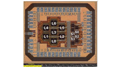
Figure 1 shows the prototype chip. It contains two matrices of hexagonal pixels with side of either r and areas corresponding to square pixels of approximately nd , respectively. The hexagonal shape of the pixels was chosen to increase the angles at the corners of the pixels, therefore reducing the electric field at the nearby surface and limit the risk of an early break-down due to the P-stop layer in the low-resistivity substrate. TCAD222https://www.synopsys.com/silicon/tcad.html simulations were used to estimate the pixel capacitance, which resulted to be approximately for the large pixel and for the small ones, for a high voltage of that provides a depletion depth of .
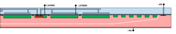
The top panel of Figure 2 shows a conceptual cross section of the detector. The P-doped substrate, in the technology standard resitivity of , is connected to the negative high voltage from the top surface outside the guard-rings and from the chip backside, while the pixels and the triple wells containing the electronics are referred to the positive low-voltage. During operation, the HV connection on the chip backside is AC coupled to ground. The chip was thinned to to reduce the resistance in series to the preamplifier input circuit. Currents below were measured when the chip was operated at bias voltages up to to take the data presented here.
Probe-station tests showed that for HV 160 V or larger a current rising up to appears after two or more days of continuous operation. This current disappears if the detector is powered off for several hours. After investigations, it was realised that this effect could be due to the very high electric field inside the shallow-trench insulation at the chip surface, which is caused by the necessity to deplete a low-resistivity silicon wafer 333This current can be eliminated by using higher-resistivity wafers that would produce a more uniform electric field. . This current is too low to affect the noise of the pixel detector and impact its timing performance.
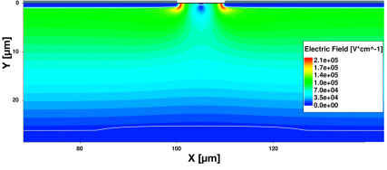
The depth of the depletion layer is not controlled by a backside P+ implantation, but it is limited by the low resistivity of the wafer. This solution greatly simplified the production of this proof-of-concept detector, although it slightly degrades the uniformity of the timing performance due to the lower electric field at the boundary between two pixels. This effect is illustrated by the TCAD simulation shown in the bottom panel of Figure 2.
1.3 SiGe HBT based front-end
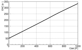
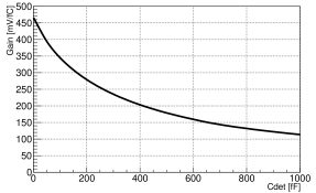
The preamplifier design is based on the one developed for the TT-PET project [3], with minor circuital adaptations to increase the gain and allow for the placement inside a deep N-well. Figure 3 shows the ENC and gain of the amplifier as predicted by Cadence Spectre simulation.
The amplifier is DC connected to a CMOS-based open-loop 3-stage discriminator. The signal from the discriminator is sent directly to the output via a low-voltage differential driver. Both the Time Of Arrival (TOA) and the Time Over Threshold (TOT) of the amplifier output can be measured from the discriminated signal. Due to the limited number of I/Os available on the chip, the pixels share four output channels, as described in Figure 1. In order to be able to turn on/off single pixels, each of them has a dedicated discrimination threshold.
2 Experimental setup and calibrations
A radioactive source, that generates photons, and a , that generates photons of 22 keV and 25 keV relevant for this study, were used to measure the performance of the preamplifier.
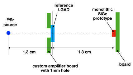
The measurement of the time resolution required the use of an LGAD detector [7] to provide a reference time. The LGAD was glued on a purposely-designed amplifier board, with a 1mm-wide opening under the LGAD to let the electrons from a source reach our chip and enable a Time-Of-Flight (TOF) measurement (see Figure 4). The reference LGAD used for this test has a time resolution of RMS [7]. To verify that the time resolution of the reference LGAD is not affected by the custom amplifier board, the TOF between two LGADs was measured using the same setup. Our measurement confirmed the time resolution found in the literature.
3 Results
3.1 Performance of the front-end electronics
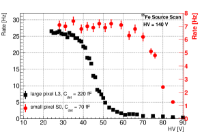
The left panel of Figure 5 shows the noise hit rate of the amplifier as a function of the discriminator threshold measured in the case of the small pixel S0 of Figure 1, both for a positive (above the baseline) and a negative threshold. The right panel of the same figure shows the noise hit rate for the large pixel L3. The noise hit rate measurements give an RMS voltage noise of and for the small and the large pixels, respectively. However, since the discriminator hysteresis acts as a filter, the actual RMS amplifier noise was obtained from Cadence Spectre simulations, and it is found to be for the small pixels and for the large ones.
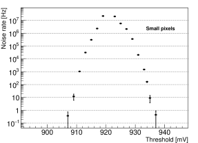
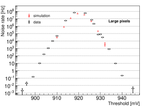
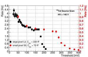
Figure 6 shows the photon hit rate as a function of the threshold measured with a and a source, for a high voltage of . The rate is approximately constant for low threshold values, indicating a good discrimination of the photon peak. The photons from the source are energetic enough to allow a rather accurate measurement of the gain, which results to be for the small pixel and for the large one.
Finally, from the measurement of the amplifier noise and the charge gain it is possible to estimate the ENC as:
which gives an ENC of 90 electrons for the small pixel and 160 electrons for the large one. This results is 30% higher than the CADENCE simulation. This discrepancy, generated by the measured values of , could be explained either by a parasitic feedback capacitance of in the amplifier circuit or by a lower voltage gain of the amplifier.
3.2 Time resolution
The electrons emitted by the source were used to measure the TOF between pixel L3 and pixel S0 of the prototype and the reference LGAD detector. For this measurement the output of the pixel under test was read by an oscilloscope with 25 Gs/s sampling rate and analogue bandwidth limited to . The remaining pixels were operated at low threshold and sent to a single channel of the oscilloscope to generate a tag signal for events with charge shared by the pixel under test and the neighbouring pixels. In the case of the large-pixel matrix, pixel L5, which shares the same output of L3, was masked.
Data were taken at several threshold and HV values. The TOF values were calculated as:
where is the time measured by the prototype chip and is the time measured by the reference LGAD. The selection cuts applied to the LGAD to obtain the sample used for the TOF were the same used for the verification of its 50 ps time resolution. No event selection was applied to the data of the prototype chip under test.
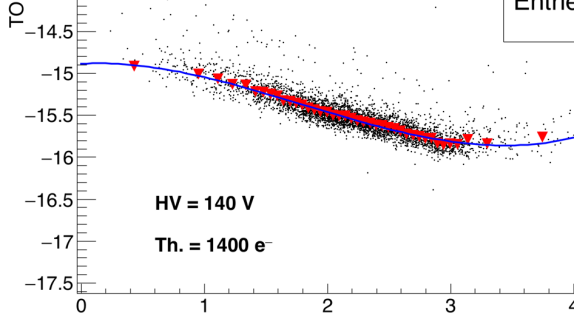
The left panels of Figure 7 show the time-walk corrections obtained for the small pixel S0 and the large pixel L3 at HV = 140 V and a threshold of 1400 and 2300 electrons, respectively. The maximum time walk is found to be less than .

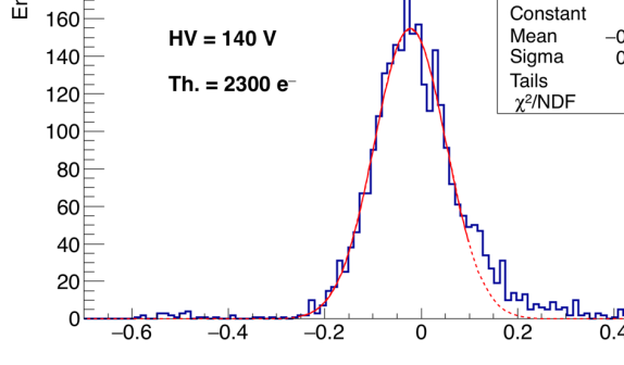
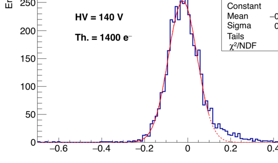
The right panels of Figure 7 show the TOF distribution for the same working points after time-walk correction. A non-Gaussian tail is observed for positive TOF values. This tail, present for all threshold and HV values, could be attributed to the electrons from the source crossing the region between two pixels and requires to be investigated in a testbeam. Gaussian fits to the time-walk corrected TOF distributions were performed to establish the time resolution of the core of the distributions. TOF times larger than +100 ps were excluded from the fits to avoid that the asymmetric tail alters the results. The time resolution of our monolithic prototype chip was calculated by subtraction in quadrature of the 50 ps time resolution contribution of the reference LGAD from the time-walk corrected TOF value. For the small pixel at the working point of Figure 7 bottom we obtain
ps
while for the large pixel at the working point of Figure 7 top the Gaussian part of the time resolution provides ps. In all instances the non-Gaussian tails were below 10 %. The negative mean value of the time-walk corrected TOF distributions is an artefact due to the fact that the time-walk corrections were calculated using all the events, including those in the tails.
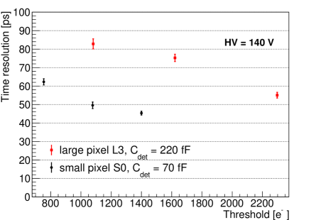
Figure 8 shows the time resolution of the prototype as a function of the discrimination threshold for the small pixel S0 and the large pixel L3 operated at HV = 140 V. For both pixel sizes the time resolution is measured to improve with increasing threshold. This observation could be explained by an improved resolution in the time-walk correction at high threshold values: the TOT, used to correct for the time walk, has a smaller error when the analogue signal crosses the discrimination threshold with a larger slope. Therefore, the present timing performance appears to be limited by the method selected to correct for the time walk.
Although the detection efficiency cannot be measured with the present experimental setup using a radioactive source, it is possible to verify that the threshold value is not cutting the measured-charge distribution above its most-probable value. The depletion depth of a silicon sensor with bulk resistivity of operated at 140 V is , which corresponds to a most probable deposited charge from a MIP of approximately 1600 electrons. Therefore, we should expect that in Figure 8 only the two higher-threshold measurements for the large pixel suffer from a significant loss in efficiency in the detection of MIPs. For the small pixel, at the intermediate threshold value, which should be close to maximal efficiency operation, the measured time resolution is ps. For a similar threshold the large pixel shows a time resolution of ps.
Figure 9 shows the dependence of the time resolution on the high voltage for the small pixel. An improvement of the time resolution is observed with increasing high voltage. This behaviour could be attributed to: i) an increase of the depletion region that provides a larger charge and a slightly lower capacitance, and therefore larger signal/noise; ii) a better uniformity of the carrier drift velocity. These limiting factors can be controlled by producing the sensor on a high resistivity epitaxial layer with a highly doped substrate.

4 Conclusions
A monolithic pixel detector prototype was produced in the IHP SiGe BiCMOS SG13G2 technology, with a sensor design optimised for timing and a fast and low-noise SiGe HBT amplifier. The prototype contains small matrices of hexagonal pixels of nd side and capacitance of approximately nd , respectively. Single-hit rate scans performed with a source indicate an ENC of the preamplifier of 90 electrons RMS and a gain of for the small pixels, and 160 electrons RMS and for the large pixels.
Data taken with a source were used to measure the TOF between the prototype and a reference LGAD detector that has 50 ps time resolution. A total excursion of the time walk below 1 ns was measured, which confirms the fast response of the amplifier. At a bias voltage of 140 V, time resolutions between ps and ps were measured at different thresholds for the smaller pixels after time-walk correction. These resolutions refer to the 90% of the events in the Gaussian core of the distributions. No event selection was performed. These results are competitive with silicon technologies that integrate an avalanche mechanism, and prove that SiGe HBT technology can provide precision tracking and excellent time resolution even in the absence of an internal gain mechanism. Experiments at beamline facilities with an external tracking system will allow for more detailed studies and for an accurate measurement of the efficiency.
Acknowledgments
The authors wish to thank Ivan Peric for several useful discussions on the sensor integration in the CMOS process, and Nicolò Cartiglia for providing the reference LGADs used in this measurement. Special thanks go to the technical staff of the DPNC of the University of Geneva for the assembly of the instrumentation and for the support during the preparation of the test. This research is based on the work performed within the TT-PET project funded by the Swiss National Science Foundation grant CRSII2-160808.
References
- [1] M. Benoit et al., 100 ps time resolution with thin silicon pixel detectors and a SiGe HBT amplifier, JINST 11 (2016) P03011, http://dx.doi.org/10.1088/1748-0221/11/03/P03011
- [2] L. Paolozzi et al., Test beam measurement of the first prototype of the fast silicon pixel monolithic detector for the TT-PET project, JINST 13 (2017) P02015, https://doi.org/10.1088/1748-0221/13/04/P04015
- [3] P. Valerio et al., A monolithic ASIC demonstrator for the Thin Time-of-Flight PET scanner, arxiv:1811.10246, accepted by JINST, https://arxiv.org/abs/1811.10246.
- [4] L. Paolozzi et al., Characterization of the demonstrator of the fast silicon monolithic ASIC for the TT-PET project., JINST 14 (2019) P02009
- [5] The TT-PET: Thin Time-of-Flight PET project, SNSF grant CRSII2-160808, http://p3.snf.ch/project-160808
- [6] H. Ruecker et al., Half-Terahertz SiGe BiCMOS technology, IEEE SiRF Symp. Dig., pp. 129-132, DOI: 10.1109/SiRF.2012.6160164, 2012.
- [7] V. Sola et al., First FBK production of 50 oltra-fast silicon detectors, NIM A 924 (2019) 360-368
- [8] L. Paolozzi, Silicon monolithic pixel detectors in a SiGe Bi-CMOS process for sub-100ps time resolution., 12th "Trento" Workshop on Advanced Silicon Radiation Detectors Oral Presentation (2017) Direct link: https://indico.cern.ch/event/587631/contributions/
- [9] C. Allaire et al., Beam test measurements of Low Gain Avalanche Detector single pads and arrays for the ATLAS High Granularity Timing Detector, JINST 13 (2018) P06017