Densities of states in Fe-doped III-V semiconductors: a first-principles study
Abstract
The electronic structures of Fe-doped III-V semiconductors were studied by first-principles supercell calculation. It was found that their electronic structures are basically the same as those of Mn-doped ones except that the extra electron of Fe compared to Mn occupies either majority-spin - hybridized antibonding states () or minority-spin states () and that the center of gravity of the partial density of states is higher for Fe than for Mn.The present calculations suggest that ferromagnetism appears when the states start to be occupied. The band splitting due to - hybridization was found to be significantly smaller than the one due to - hybridization. This indicates that the - exchange interaction is not responsible for the high-temperature ferromagnetism of the Fe-doped ferromagnetic semiconductors even in -type compounds.
pacs:
Valid PACS appear hereI Introduction
Ferromagnetic semiconductors (FMSs) have been studied extensively for decades since the discovery of Mn-doped III-V FMSs Munekata et al. (1989); Ohno et al. (1996); Jungwirth et al. (2014); Dietl and Ohno (2014); Tanaka et al. (2014); Dietl et al. (2015). More recently, Fe-doped FMSs were synthesized Nam Hai et al. (2012a); Tu et al. (2014); Anh et al. (2015); Tu et al. (2018); Wakabayashi et al. (2014) and have attracted much interest because they possess several advantages over the prototypical (Ga,Mn)As or (In,Mn)As. First of all, the Curie temperatures () are very high. Especially, the ’s of (Ga,Fe)Sb and (In,Fe)Sb are 340 K Tu et al. (2016) and 335 K Tu et al. (2018) at highest, respectively, exceeding not only the highest K of (Ga,Mn)As Chen et al. (2011) but also room temperature. Second, various types of transport properties are realized: -type semiconducting for (Ga,Fe)Sb Tu et al. (2014) and Ge:Fe Ban et al. (2014), -type semiconducting for (In,Fe)As:Be Nam Hai et al. (2012a) and (In,Fe)Sb Tu et al. (2018), and insulating for (Al,Fe)Sb Anh et al. (2015). However, the basic electronic structure and the mechanism of the ferromagnetism as well as the origin of the diverse transport properties remain unclear and should be revealed for further development in this direction.
First-principles calculation based on density functional theory (DFT) is a powerful method for such a purpose, and has been widely used to study the electronic structures of FMSs Jungwirth et al. (2006); Sato et al. (2010). Although it is difficult to exactly simulate randomly doped systems, a supercell approach provides the useful information about the basic electronic structures and the magnetic properties Sato and Katayama-Yoshida (2000); Sandratskii and Bruno (2002); Shick et al. (2004); Wierzbowska et al. (2004); Filippone et al. (2011). In the present study, we have constructed supercells and calculated the electronic structure or the density of states (DOS) of newly-discovered Fe-doped III-V FMSs as well as the spin and orbital magnetic moments.
II Methods
| Unit cell | [Å] | ||||
|---|---|---|---|---|---|
| 5.4672 | 2.5 | 2.33 | 1.95 | 5.5 | |
| 5.4505 | 2.49 | 2.44 | 1.94 | 5.5 | |
| 5.8697 | 2.5 | 2.5 | 2.09 | 5.5 | |
| 5.6611 | 2.36 | 2.19 | 2.24 | 6.5 | |
| 5.6533 | 2.36 | 2.3 | 2.24 | 7.5 | |
| 6.0583 | 2.5 | 2.5 | 2.4 | 7.5 | |
| 6.1355 | 2.49 | 2.3 | 2.49 | 6.5 | |
| 6.0959 | 2.47 | 2.41 | 2.47 | 7.5 | |
| 6.4794 | 2.5 | 2.5 | 2.5 | 8 |
DFT calculations were done using the all-electron full-potential (linearized) augmented-plane-wave plus local-orbital method implemented in a WIEN2k package Blaha et al. (2001). The spherical harmonic expansion was made up to inside the muffin-tin spheres. The plane wave cutoff () and the radii of MT spheres are summarized in Table 1. For the exchange-correlation energy functional, the Perdew-Burke-Ernzerhof (PBE) generalized gradient approximation (GGA) was used Perdew et al. (1996). In order to simulate the randomly doped system, supercells consisting of 3 3 3 primitive unit cell of the zinc blende structure are employed as shown at the top left corner of Fig. 1, which contain 27 group-V atoms, 26 group-III atoms, and 1 Fe atom. This corresponds to Fe doping and would be a good starting point to study the basic electronic structure of isolated Fe atoms in III-V matrix without significant Fe-Fe interaction or hybridization. Brillouin-zone integration was performed on a 4 4 4 -point mesh. The experimental lattice constants of host semiconductors Vurgaftman et al. (2001) were used for all the calculations for simplicity. The self-consistent cycle was repeated until the calculated total energy converged to within 0.0001 Ry per supercell.
III Results
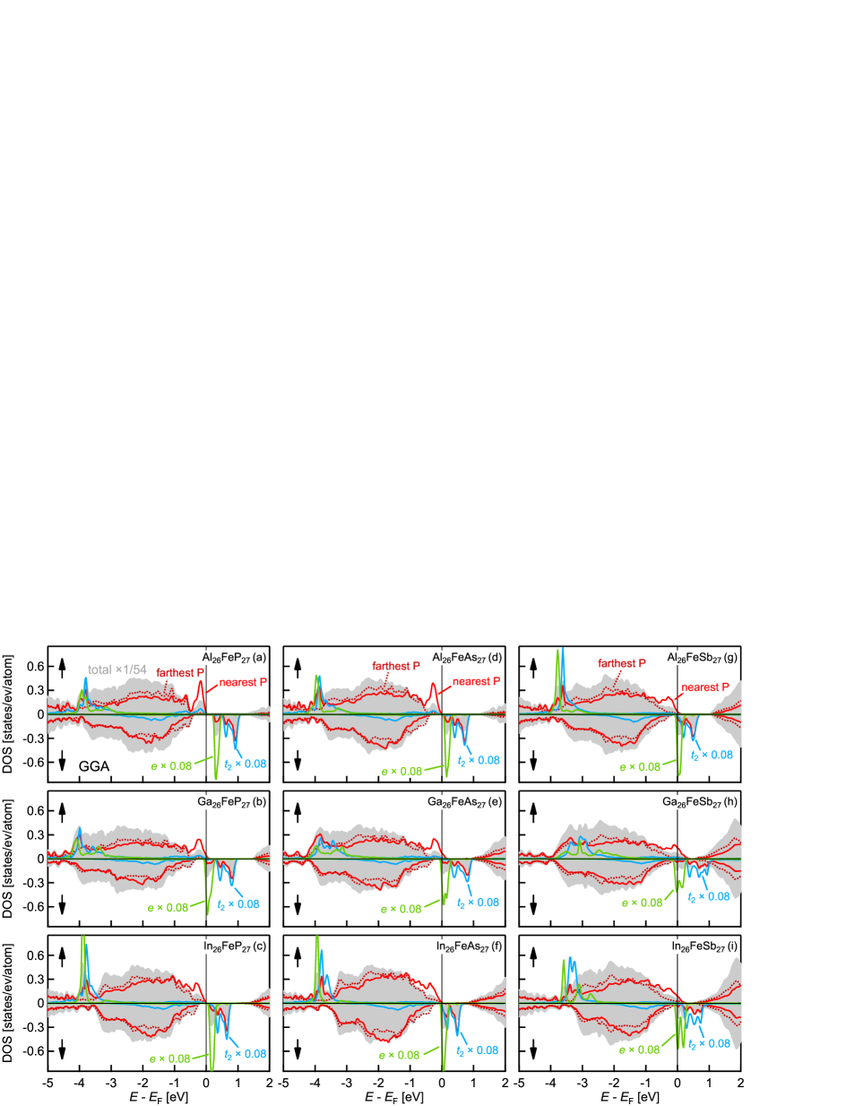
Figure 2 shows the spin-resolved total DOSs and partial DOSs (PDOSs) of Fe-doped III-V semiconductors. The total DOSs are indicated by gray areas, and the PDOSs of the group-V atoms located nearest to and farthest from the Fe atom are shown by red solid and dashed curves, respectively. The PDOSs of Fe (,,) and (,) orbitals are also shown by blue and green curves. For the sake of easy comparison, the total DOS is divided by 54 (the total number of atoms in the supercell), and the PDOSs of and orbitals are multiplied by 0.08. Note that the (P)DOSs of majority-spin and minority-spin states are shown at the positive and negative sides of each panel.
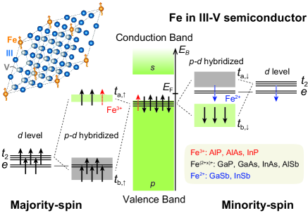
Reflecting the calculated DOSs, the schematic energy diagram is illustrated in Fig. 1. The valence and conduction bands, mainly consisting of the orbital of the group V element and the orbital of group III element, respectively, are shown in the middle of the figure by green boxes, while the majority-spin and minority-spin 3 levels are shown on the left- and right-hand side, respectively. The 3 levels split into doubly-degenerate lower state and triply-degenerate higher state because of the tetrahedral crystal field at the substitutional sites of group-III element in the zinc-blende crystal. Furthermore, the orbitals and the ligand orbitals strongly hybridize with each other and form bonding and antibonding orbitals. The majority-spin bonding states () of predominant character are located deep about 3-4 eV below the Fermi energy (), while the antibonding states () of predominant character are near the valence-band maximum. On the other hand, the minority-spin bonding states () mainly consisting of the ligand orbitals form part of the valence band, and antibonding states () of character remain unoccupied. Note that the orbitals do not strongly hybridize with the ligand orbitals.
In the case of the prototypical Mn-doped III-V systems, the level crosses the accommodating a hole, because the substitution of Mn with the configuration for group III element with makes one electron missing from the valence band. On the other hand, in the case of the Fe-doped III-V system, the states would be fully occupied since Fe has one more electron than Mn and can take the configuration. In the present calculation, this is the case for (Al,Fe)P, (Al,Fe)As, and (In,Fe)P. To be precise, the Fe and the ligand orbitals take the configuration in those cases, while Mn in III-V semiconductors takes the configuration. (Ga,Fe)Sb and (In,Fe)Sb, however, showed distinct behavior from this. That is, Fe and the ligand take the configuration, where an electron occupies the state instead of the . This is probably because the valence band or the level of GaSb and InSb lies rather high in energy Vurgaftman et al. (2001), and it becomes more stable for an electron to occupy the than to occupy the states. The former electronic configuration is denoted as Fe3+ hereafter, and the latter configuration as Fe2+. The other systems such as (Ga,Fe)As and (Al,Fe)Sb lie between Fe3+ and Fe2+, i.e., a small amount of electrons occupies the states and a small amount of holes are introduced to the states accordingly. This is represented by red and blue dashed arrows in Fig. 1, where the electron of highest energy occupies either or levels.
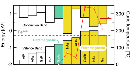
This situation is illustrated in Fig. 3, where the band offsets of III-V semiconductors Vurgaftman et al. (2001) and Ge Franciosi and de Walle (1996) are shown. The dashed line approximately represents the energy level above which the Fe2+ configuration is stabilized. For example, in GaAs, the position of the dashed line shows the Fe3+/2+ charge transfer level Malguth et al. (2008). The highest ever achieved for each material is also plotted. Considering that (Ga,Fe)As is paramagnetic Haneda et al. (2000); Moriya et al. (2001), while the other Fe-doped semiconductors whose valence band maximum is located higher in energy than that of GaAs are ferromagnetic, ferromagnetism might appear when the Fe level starts being occupied.
The strength of the - exchange or the spin splitting of the valence band caused by - hybridization can be approximated as , where denotes the transfer integral between the ligand and the Fe orbitals, and and the energy level of the majority-spin ligand and the Fe orbitals without the hybridization. For example, as the host semiconductor changes from AlP GaP InP, the - hybridization becomes weaker because the increase in the lattice constant leads to the decrease in and the higher energy position of the valence band () results in the increase in . This trend also holds for AlAs GaAs InAs series and basically for AlSb GaSb InSb series, too. Table 2 summarizes the spin splitting of the valence band () and that of the conduction band () obtained as the leading-edge difference between the majority- and minority-spin valence-band and conduction-band DOSs. In fact, decreased as (Al,Fe)X (Ga,Fe)X (In,Fe)X, where X denotes P, As, or Sb.
The spin splitting of the conduction band is significantly smaller than that of the valence band since - hybridization is very weak compared to the - hybridization. A recent tunneling spectroscopy study Le Duc Anh and Tanaka (2016) on ferromagnetic (In,Fe)As revealed that the splitting of the conduction band was 31.7 and 50 meV for 6% and 8% Fe doping, respectively. These values agree with the calculated one of 20 meV for 3.7% Fe doping, because the is calculated to be 0.22 eV assuming and is almost the same as the experimental 0.21-0.25 eV.
Table 2 also shows the calculated spin and orbital magnetic moments of Fe atom, and the total magnetic moment of the 333 supercell. Because of the strong - hybridization, a sizable amount of 3 electrons also occupies states. This results in the smaller magnetic moment of Fe atoms than the ionic value of 5 . Nevertheless, in the system with the empty level such as (Al,Fe)P or (In,Fe)P, the total magnetic moment of the supercell is exactly 5 . Similar behavior was also reported for (Ga,Mn)As Shick et al. (2004), where the DFT calculation based on the local spin-density approximation (LSDA) yielded the Mn moment of 3.47 , while the total magnetic moment in the supercell is exactly 4 . In the case of (Ga,Fe)Sb and (In,Fe)Sb, where an extra electron occupies the states instead of the , the total magnetic moment in the supercell is reduced by 1 . The intermediate systems such as (Ga,Fe)As or (Al,Fe)Sb showed the total magnetic moment slightly smaller than 5 . Note that the number of 3 electrons is 6 for all the systems studied in the present work.
The orbital magnetic moment relative to the spin magnetic moment () increases from 0.015 to 0.061 as a host semiconductor becomes heavier and spin-orbit interaction becomes stronger. This is consistent with the previous x-ray magnetic circular dichroism (XMCD) experiments, where / is 0.1 for (In,Fe)As Sakamoto et al. (2016) and 0.13 for (Ga,Fe)Sb Sakamoto et al. (2019).
| material | / | ||||
|---|---|---|---|---|---|
| [/Fe] | [/cell] | [eV] | [eV] | ||
| (Al,Fe)P | 3.33 | 0.015 | 5.00 | 0.41 | 0.08 |
| (Ga,Fe)P | 3.31 | 0.016 | 4.91 | 0.32 | 0.04 |
| (In,Fe)P | 3.51 | 0.017 | 5.00 | 0.21 | 0.02 |
| (Al,Fe)As | 3.33 | 0.023 | 4.97 | 0.34 | 0.06 |
| (Ga,Fe)As | 3.37 | 0.024 | 4.76 | 0.23 | 0.03 |
| (In,Fe)As | 3.48 | 0.027 | 4.96 | 0.22 | 0.02 |
| (Al,Fe)Sb | 3.29 | 0.043 | 4.89 | 0.28 | 0.04 |
| (Ga,Fe)Sb | 3.06 | 0.049 | 3.69 | 0.34 | 0.04 |
| (In,Fe)Sb | 3.30 | 0.061 | 4.16 | 0.25 | 0.03 |
IV Discussion
There are three kinds of exchange interactions often discussed in the field of dilute ferromagnetic semiconductors, namely, ,- exchange interaction, double-exchange interaction, and superexchange interaction. ,- exchange interaction, which has been applied to the Mn-doped FMSs, does not seem very important for the Fe-doped FMSs for the following reasons. First, the Curie temperatures of -type (In,Fe)As Nam Hai et al. (2012a) and (In,Fe)Sb Tu et al. (2018) are similar to, or even higher than, that of -type (Ga,Fe)Sb Tu et al. (2015) despite the fact that - exchange interaction is an order of magnitude weaker than - exchange interaction as seen from Table 2, which indicated that . Second, ferromagnetism with = 40 K was also reported for insulating (Al,Fe)Sb, whose carrier concentration was 3 1017 cm-3, three to four orders of magnitude smaller than that of (Ga,Mn)As Anh et al. (2015). Third, it was recently shown that the ferromagnetism of (In,Fe)Sb is not significantly influenced by carrier concentration and even by carrier type Kudrin et al. (2019).
Superexchange interaction is very short-ranged and antiferromagnetic for the nearest-neighbor Fe pairs and is often treated as obstacles for ferromagnetism in FMSs. Shinya . Shinya et al. (2018) pointed out that the second-nearest-neighbor superexchange interaction is actually ferromagnetic for (Ga,Fe)Sb and (In,Fe)Sb, although the magnitude of the interaction was too small to account for their high s.
If the Fe2+ state is realized, there can also be double-exchange interaction between partly-filled orbitals. Such a scenario was proposed in the theoretical calculation on (In,Fe)As:Be done by Vu . Vu et al. (2014), where they claimed that extra electrons introduced by Be doping occupy the orbitals and can induce a ferromagnetic order. The fact that the tends to be higher in Sb based material, where the calculation yielded the Fe2+ state rather than Fe3+, may suggest that double-exchange interaction is more likely to be responsible for the ferromagnetic order.
It is worth mentioning that there might be a long-range exchange interaction between the orbitals and the host bands both in - and -type semiconductors especially if they have narrow band gaps Gu and Maekawa (2016). Such an interaction might be resonantly enhanced when orbitals and host bands are close in energy as suggested by Hai et al. Nam Hai et al. (2012b) and may also play a role in stabilizing long-range ferromagnetic order.
Considering the low concentrations of Fe atoms doped into the host semiconductors, it appears necessary to think about the inhomogeneous distribution of Fe atoms on the nanoscale, or the spinodal nanodecomposition Dietl et al. (2015), because both superexchange and double-exchange interactions are short-ranged. In fact, previous XMCD measurements on (In,Fe)As:Be Sakamoto et al. (2016) and (Al,Fe)Sb Sakamoto et al. thin films grown by the molecular beam epitaxy methods revealed that there exist nanoscale ferromagnetic domains even at room temperature much above the macroscopic , the origin of which was attributed to the nanoscale Fe concentration fluctuation. Furthermore, the nanoscale Fe-rich lamellae-like structures were recently observed in (In,Fe)As thin films prepared by the pulsed laser melting method Yuan et al. (2018). From theoretical points of view, it has been shown that it is more energetically stable for Fe atoms to be distributed close to each other in (In,Fe)As:Be Yuan et al. (2018) (especially in the presence of interstitial Be atoms Vu et al. (2014)), (Ga,Fe)Sb, and (In,Fe)Sb Shinya et al. (2018); Fukushima et al. (2019). Note that, in every study mentioned above, Fe atoms do not precipitate but maintain the zinc-blende structure. When such Fe-rich regions are formed and become locally highly metallic, it may be even possible that Stoner ferromagnetism emerges in those regions.
The transport property would be another puzzle if one assume the Fe2+ configuration. This should introduce as many hole carriers as doped Fe atoms, but in reality, the carrier concentration is orders of magnitude smaller than the doped Fe atoms. This discrepancy would be resolved if one assumes that the carriers are trapped inside the Fe-rich regions and macroscopic carrier transport occurs via hopping between those Fe-rich regions. Such a model was originally introduced by Kaminski and Das Sarma for (Ga,Mn)As Kaminski and Das Sarma (2003) and subsequently applied to Ge:Mn Pinto et al. (2005), Ge:Fe Ban et al. (2018), and (Zn,Cr)Te Sreenivasan et al. (2007) to describe their insulating/semiconducting natures and measured low carrier concentrations (1018 cm-3 for Ge:Mn Pinto et al. (2005) and Ge:Fe Ban et al. (2014), 1015 cm-3 for (Zn,Cr)Te Saito et al. (2002)).
We have not calculated how interstitial Fe atoms alter the electronic structure, but there would be two major effects. First, the electron carrier concentration would increase because interstitial Fe atoms would act as double/triple donors. Second, there might be a reduction in the net magnetization because interstitial Fe atoms would probably be antiferromagnetically coupled to adjacent Fe atoms. Although such effects should be rigorously assessed both theoretically and experimentally in future studies, they may be ignored in the first approximation considering orders of magnitude lower carrier concentration than the number of doped Fe atoms.
V Conclusion
We have calculated the basic electronic structures of Fe-doped III-V semiconductors by first-principles supercell calculation. They were found to be similar to those of Mn-doped counterparts except that one more electron of Fe than Mn occupies either majority-spin antibonding states () or minority-spin states () and that the center of gravity of the partial density of states is higher for Fe than for Mn. The is preferentially occupied in the cases of (Ga,Fe)Sb and (In,Fe)Sb, where the level or the valence band is located high in energy and, therefore, it is more stable for the electron to occupy states than states. As the group-III element changes from Al Ga In, - exchange interaction gets weaker because the increase of Fe-V bond length leads to the decrease of the transfer integral between the Fe orbitals and ligand orbitals. As the group-V element changes from P As Sb, - exchange interaction also becomes weaker because more covalent nature and higher energy position of level makes larger. The present calculations implied that the ferromagnetism originates from the nanoscale fluctuation of Fe atom distribution, otherwise the small amount of carriers is not likely to stabilize the long-range ferromagnetic order especially in the case of -type (In,Fe)As and (In,Fe)Sb and insulating (Al,Fe)Sb.
acknowledgments
This work was supported by Grants-in-Aids for Scientific Research from the JSPS (No. 15H02109). A.F. is an adjunct member of the Center for Spintronics Research Network (CSRN), the University of Tokyo, under Spintronics Research Network of Japan (Spin-RNJ). S.S. acknowledges financial support from Advanced Leading Graduate Course for Photon Science (ALPS) and the JSPS Research Fellowship for Young Scientists.
References
- Munekata et al. (1989) H. Munekata, H. Ohno, S. von Molnar, A. Segmüller, L. L. Chang, and L. Esaki, Phys. Rev. Lett. 63, 1849 (1989).
- Ohno et al. (1996) H. Ohno, A. Shen, F. Matsukura, A. Oiwa, A. Endo, S. Katsumoto, and Y. Iye, Appl. Phys. Lett. 69, 363 (1996).
- Jungwirth et al. (2014) T. Jungwirth, J. Wunderlich, V. Novák, K. Olejník, B. L. Gallagher, R. P. Campion, K. W. Edmonds, A. W. Rushforth, A. J. Ferguson, and P. Němec, Rev. Mod. Phys. 86, 855 (2014).
- Dietl and Ohno (2014) T. Dietl and H. Ohno, Rev. Mod. Phys. 86, 187 (2014).
- Tanaka et al. (2014) M. Tanaka, S. Ohya, and P. Nam Hai, Appl. Phys. Rev. 1, 011102 (2014).
- Dietl et al. (2015) T. Dietl, K. Sato, T. Fukushima, A. Bonanni, M. Jamet, A. Barski, S. Kuroda, M. Tanaka, P. N. Hai, and H. Katayama-Yoshida, Rev. Mod. Phys. 87, 1311 (2015).
- Nam Hai et al. (2012a) P. Nam Hai, L. Duc Anh, S. Mohan, T. Tamegai, M. Kodzuka, T. Ohkubo, K. Hono, and M. Tanaka, Appl. Phys. Lett. 101, 182403 (2012a).
- Tu et al. (2014) N. T. Tu, P. N. Hai, L. D. Anh, and M. Tanaka, Appl. Phys. Lett. 105, 132402 (2014).
- Anh et al. (2015) L. D. Anh, D. Kaneko, P. N. Hai, and M. Tanaka, Appl. Phys. Lett. 107, 232405 (2015).
- Tu et al. (2018) N. T. Tu, P. N. Hai, L. D. Anh, and M. Tanaka, Appl. Phys. Express 11, 063005 (2018).
- Wakabayashi et al. (2014) Y. K. Wakabayashi, Y. Ban, S. Ohya, and M. Tanaka, Phys. Rev. B 90, 205209 (2014).
- Tu et al. (2016) N. T. Tu, P. N. Hai, L. D. Anh, and M. Tanaka, Appl. Phys. Lett. 108, 192401 (2016).
- Chen et al. (2011) L. Chen, X. Yang, F. Yang, J. Zhao, J. Misuraca, P. Xiong, and S. von Molnár, Nano Lett. 11, 2584 (2011).
- Ban et al. (2014) Y. Ban, Y. Wakabayashi, R. Akiyama, R. Nakane, and M. Tanaka, AIP Adv. 4, 097108 (2014).
- Jungwirth et al. (2006) T. Jungwirth, J. Sinova, J. Mašek, J. Kučera, and A. H. MacDonald, Rev. Mod. Phys. 78, 809 (2006).
- Sato et al. (2010) K. Sato, L. Bergqvist, J. Kudrnovský, P. H. Dederichs, O. Eriksson, I. Turek, B. Sanyal, G. Bouzerar, H. Katayama-Yoshida, V. A. Dinh, T. Fukushima, H. Kizaki, and R. Zeller, Rev. Mod. Phys. 82, 1633 (2010).
- Sato and Katayama-Yoshida (2000) K. Sato and H. Katayama-Yoshida, Jpn. J. Appl. Phys. 39, L555 (2000).
- Sandratskii and Bruno (2002) L. M. Sandratskii and P. Bruno, Phys. Rev. B 66, 134435 (2002).
- Shick et al. (2004) A. B. Shick, J. Kudrnovský, and V. Drchal, Phys. Rev. B 69, 125207 (2004).
- Wierzbowska et al. (2004) M. Wierzbowska, D. Sánchez-Portal, and S. Sanvito, Phys. Rev. B 70, 235209 (2004).
- Filippone et al. (2011) F. Filippone, G. Mattioli, P. Alippi, and A. A. Bonapasta, Phys. Rev. Lett. 107, 196401 (2011).
- Blaha et al. (2001) P. Blaha, K. Schwarz, G. Madsen, D. Kvasnicka, and J. Luitz, An augmented plane wave+ local orbitals program for calculating crystal properties (2001).
- Perdew et al. (1996) J. P. Perdew, K. Burke, and M. Ernzerhof, Phys. Rev. Lett. 77, 3865 (1996).
- Vurgaftman et al. (2001) I. Vurgaftman, J. R. Meyer, and L. R. Ram-Mohan, J. Appl. Phys. 89, 5815 (2001).
- Franciosi and de Walle (1996) A. Franciosi and C. G. V. de Walle, Surf. Sci. Rep. 25, 1 (1996).
- Malguth et al. (2008) E. Malguth, A. Hoffmann, and M. R. Phillips, Phys. Status Solidi B 245, 455 (2008).
- Haneda et al. (2000) S. Haneda, M. Yamaura, Y. Takatani, K. Hara, S. ichi Harigae, and H. Munekata, Jpn. J. Appl. Phys. 39, L9 (2000).
- Moriya et al. (2001) R. Moriya, Y. Katsumata, Y. Takatani, S. Haneda, T. Kondo, and H. Munekata, Physica E: Low-dimensional Systems and Nanostructures 10, 224 (2001), proceedings of the First International Conference on the Physics and Applications of Spin-Related Phenomena in Semiconductors.
- Le Duc Anh and Tanaka (2016) P. N. H. Le Duc Anh and M. Tanaka, Nat. Commun. 7 (2016).
- Sakamoto et al. (2016) S. Sakamoto, L. D. Anh, P. N. Hai, G. Shibata, Y. Takeda, M. Kobayashi, Y. Takahashi, T. Koide, M. Tanaka, and A. Fujimori, Phys. Rev. B 93, 035203 (2016).
- Sakamoto et al. (2019) S. Sakamoto, N. T. Tu, Y. Takeda, S.-i. Fujimori, P. N. Hai, L. D. Anh, Y. K. Wakabayashi, G. Shibata, M. Horio, K. Ikeda, Y. Saitoh, H. Yamagami, M. Tanaka, and A. Fujimori, Phys. Rev. B 100, 035204 (2019).
- Tu et al. (2015) N. T. Tu, P. N. Hai, L. D. Anh, and M. Tanaka, Phys. Rev. B 92, 144403 (2015).
- Kudrin et al. (2019) A. Kudrin, V. Lesnikov, Y. Danilov, M. Dorokhin, O. Vikhrova, D. Pavlov, Y. Usov, I. Antonov, R. Kriukov, S. Zubkov, D. Nikolichev, A. Konakov, Y. Dudin, Y. Kuznetsov, M. Temiryazeva, and N. Sobolev, J. Magn. Magn. Mater. 485, 236 (2019).
- Shinya et al. (2018) H. Shinya, T. Fukushima, A. Masago, K. Sato, and H. Katayama-Yoshida, J, Appl. Phys. 124, 103902 (2018).
- Vu et al. (2014) N. D. Vu, T. Fukushima, K. Sato, and H. Katayama-Yoshida, Jpn. J. Appl. Phys. 53, 110307 (2014).
- Gu and Maekawa (2016) B. Gu and S. Maekawa, Phys. Rev. B 94, 155202 (2016).
- Nam Hai et al. (2012b) P. Nam Hai, L. D. Anh, and M. Tanaka, Appl. Phys. Lett. 101, 252410 (2012b).
- (38) S. Sakamoto, L. D. Anh, P. N. Hai, Y. Takeda, M. Kobata, R. Nakane, Y. K. Wakabayashi, Y. Nonaka, K. Ikeda, Z. Chi, Y. Wan, M. Suzuki, Y. Saitoh, H. Yamagami, M. Tanaka, and A. Fujimori, arXiv:1902.03742 .
- Yuan et al. (2018) Y. Yuan, R. Hübner, M. Birowska, C. Xu, M. Wang, S. Prucnal, R. Jakiela, K. Potzger, R. Böttger, S. Facsko, J. A. Majewski, M. Helm, M. Sawicki, S. Zhou, and T. Dietl, Phys. Rev. Mater. 2, 114601 (2018).
- Fukushima et al. (2019) T. Fukushima, H. Shinya, A. Masago, K. Sato, and H. Katayama-Yoshida, Appl. Phys. Express 12, 063006 (2019).
- Kaminski and Das Sarma (2003) A. Kaminski and S. Das Sarma, Phys. Rev. B 68, 235210 (2003).
- Pinto et al. (2005) N. Pinto, L. Morresi, M. Ficcadenti, R. Murri, F. D’Orazio, F. Lucari, L. Boarino, and G. Amato, Phys. Rev. B 72, 165203 (2005).
- Ban et al. (2018) Y. Ban, Y. K. Wakabayashi, R. Nakane, and M. Tanaka, J. Appl. Phys. 124, 113902 (2018).
- Sreenivasan et al. (2007) M. G. Sreenivasan, K. L. Teo, X. Z. Cheng, M. B. A. Jalil, T. Liew, T. C. Chong, A. Y. Du, T. K. Chan, and T. Osipowicz, J. Appl. Phys. 102, 053702 (2007).
- Saito et al. (2002) H. Saito, W. Zaets, S. Yamagata, Y. Suzuki, and K. Ando, J. Appl. Phys. 91, 8085 (2002).