On-chip polarization rotator for type I second harmonic generation
Abstract
We demonstrate a polarization rotator integrated at the output of a GaAs waveguide producing type I second harmonic generation (SHG). Form-birefringent phase matching between the pump fundamental transverse electric (TE) mode near 2.0 m wavelength and the signal fundamental transverse magnetic (TM) mode efficiently generates light at 1.0 m wavelength. A SiN waveguide layer is integrated with the SHG device to form a multi-functional photonic integrated circuit. The polarization rotator couples light between the two layers and rotates the polarization from TM to TE or from TE to TM. With a TE-polarized 2.0 m pump, type I SHG is demonstrated with the signal rotated to TE polarization. Passive transmission near 1.0 m wavelength shows 80 % polarization rotation across a broad bandwidth of 100 nm. By rotating the signal polarization to match that of the pump, this SHG device demonstrates a critical component of an integrated self-referenced octave-spanning frequency comb. This device is expected to provide crucial functionality as part of a fully integrated optical frequency synthesizer with resolution of less than one part in 1014.
I Introduction
Second harmonic generation (SHG) is an important nonlinear process for stabilizing the carrier-envelope offset frequency of an octave-spanning frequency comb. This process, known as - self-referencing, produces a stable frequency reference that finds various uses for timing Nicklaus et al. (2017); Francis et al. (2018) as well as for frequency synthesis. Integrated versions of - self-referencing are currently under development and are expected to open new applications for this technology Spencer et al. (2018); Newman et al. (2019); Malinowski et al. (2019). Devices that produce efficient SHG are generally also suitable for efficient parametric down-conversion (PDC), an enabling process for integrated quantum photonic systems Guo et al. (2017); Atzeni et al. (2018); Singh et al. (2019).
A common approach for - self-referencing is to compare the 2.0 m and 1.0 m parts of a frequency comb using SHG Volet et al. (2018); Suh et al. (2019); Briles et al. (2018); Gaeta, Lipson, and Kippenberg (2019). For this technique, octave spanning dissipative Kerr solitons are readily synthesized using a 1.55 m pump Volet et al. (2018); Huang et al. (2019).
High conversion efficiency SHG has recently been demonstrated in GaAs Chang et al. (2018, 2019); Stanton et al. (2019) and AlGaAs May et al. (2019) waveguides using form birefringence phase matching Fiore et al. (1998a, b) and in periodically-poled LiNbO3 Wang et al. (2018); Desiatov et al. (2019) waveguides using quasi-phase matching. Additionally, AlGaAs platforms Pu et al. (2016); Liu et al. (2019); Zheng et al. (2018); Chiles et al. (2019) have demonstrated frequency combs and supercontinuum generation with high efficiency. Type I SHG in either GaAs or AlGaAs is a promising platform for efficient SHG from 2 m to 1 m because of the strong nonlinearity Skauli et al. (2002) and small mode sizes. Recently, we demonstrated SHG conversion efficiency of 130 W-1cm-2 in GaAs waveguides Chang et al. (2018). However, this process results in a signal and pump having orthogonal polarization, preventing self-referencing. The octave-spanning comb is typically generated in the fundamental transverse electric (TE) mode, and the SHG process is also most efficient with a fundamental TE mode pump. Therefore, a polarization rotator is needed to rotate the SHG signal from transverse magnetic (TM) to TE.
An exemplary polarization rotator has minimal loss and supports a broad bandwidth with tolerance to fabrication error. This can be achieved with a passive device. Coupling between TE and TM polarizations can be either resonant or adiabatic, with resonant coupling producing a much smaller device and adiabatic coupling supporting a larger bandwidth Wang and Dai (2008); Dai and Bowers (2011). In both cases, the mode coupling between polarizations can be realized by introducing an asymmetry in the waveguide cross-section, either horizontally, vertically, or both. Vertical asymmetry can be engineered by creating an upper and lower cladding with different materials. Horizontal asymmetry is typically formed by partially etching the waveguide core Wang and Dai (2008) or by bending the waveguide Obayya et al. (2001). Using both horizontal and vertical asymmetry is advantageous for adiabatic polarization rotation because the waveguides can be designed with a stronger mode hybridization between the fundamental TE and TM modes and thus support a shorter rotator length. Polarization rotation can also be designed by coupling the fundamental TM mode to the first higher order TE mode and then separately coupling the first order TE mode to the fundamental TE mode Dai and Bowers (2011); Sacher et al. (2014). These devices are robust to fabrication error and support efficient polarization rotation, but a single stage of polarization rotation between the fundamental TE and TM modes is preferred to reduce the size and complexity of the device.
Here we report a type I SHG waveguide integrated with a passive polarization rotator. The design produces a high polarization rotation from the fundamental TM to the fundamental TE mode in a single coupling stage. Two sets of measurements are performed to characterize the device. First, SHG is demonstrated with a TE-polarized 2 m pump to produce a TE-polarized signal at the output of the chip. This confirms the polarization rotator efficiently converts the TM-polarized signal to the TE polarization. Second, the bandwidth of our polarization rotator is characterized by transmission measurements at 1 m.
II Design
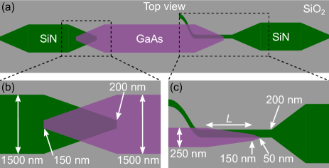
By integrating both a SiN and a GaAs waveguide, we have broad flexibility in the design to introduce both vertical and horizontal asymmetry. The thickness of the SiN layer is 400 nm to provide a balance between sufficient confinement at the 2.0 m wavelength and efficient coupling between the SiN and GaAs layers at the 1 m wavelength. This SiN layer can also support additional photonic elements necessary for - self-referencing. The GaAs waveguide is 150 nm thick and 1500 nm wide in the straight section, which is designed for phase-matching with a 2.0 m pump. The complete polarization rotator schematic is shown in Fig. 1(a). It consists of a SiN waveguide at the input, an input SiN-GaAs coupler, a GaAs SHG waveguide, an output GaAs-SiN coupler, and an output SiN waveguide.
The input coupler dimensions are shown in Fig. 1(b). Along the length, the cross-section is horizontally symmetric and the GaAs waveguide tapers from 150 nm to 1500 nm while the SiN waveguide tapers from 1500 nm to 200 nm. An eigenmode expansion calculation estimates high transmission of 95 % at 2 m wavelength from the fundamental TE mode of the SiN waveguide to the fundamental TE mode of the GaAs waveguide. A reference device is designed with the inverse of this input coupler at its output, instead of the polarization rotator, coupling the fundamental TM mode of the 1 m signal from the GaAs waveguide to the fundamental TM mode of the SiN waveguide. Transmission of 80 % is calculated for this output taper.
The output GaAs-SiN coupler designed for polarization rotation is shown in Fig. 1(c). Rotation occurs in an 800 m long region of the device where the GaAs tapers in width from 250 nm to 150 nm and the SiN waveguide width is fixed at 400 nm. Throughout the taper, the center of the GaAs waveguide is located at one edge of the SiN waveguide to create the horizontal asymmetry. Prior to this region, the SiN waveguide is gradually introduced to the 250 nm wide GaAs waveguide using an s-bend. After the rotator, the GaAs waveguide is terminated by tapering the width down to a 50 nm tip over a 20 m length.
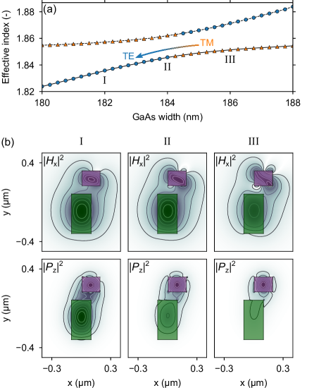
With an optimized geometry, we find a condition where the fundamental TE and TM modes hybridize and exhibit strong coupling. This is shown in Fig. 2(a) where the effective indices of the first two guided modes are plotted against the GaAs waveguide width. The gap between the fundamental mode and the first higher order mode indicates a hybrid TEM mode at a GaAs waveguide width of 184 nm. Strong coupling between the TE and TM modes is possible by tapering the GaAs width through this point. The simulated indices indicated with blue circles represent a TE polarization fraction of greater than 50 % and the orange triangles correspond to less than 50 %. This mode polarization value is defined as . The mode profiles shown in Fig. 2(b) correspond to the GaAs widths from Fig. 2(a) as indicated by the Roman numerals. The x-component of the magnetic field shows how the polarization rotates and the z-component of the power shows how light is vertically coupling from the GaAs to the SiN as the GaAs width decreases.
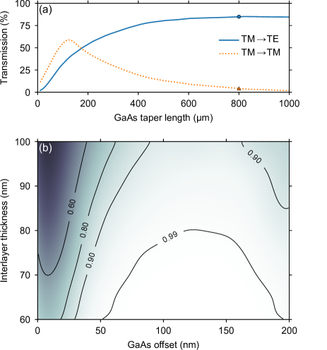
For a GaAs width taper from 250 nm to 150 nm, the transmission is simulated from an input TM mode in Fig. 3(a) to the output TE and TM modes for taper lengths between 0 m and 1000 m. Efficient polarization rotation is found for a length of 800 m, which is the nominal value used for the rotator length. One of the advantages of our design approach is its tolerance to fabrication errors. In particular, two parameters are expected to have relatively large fabrication error: the alignment between the GaAs and SiN waveguide layers and the SiO2 spacer thickness between the GaAs and SiN waveguide layers. The polarization rotation, defined as for a TM input where is the ratio of the TE/TM polarized output power to the input power, is simulated for a layer misalignment in the range of 100 nm and a spacer thickness error in the range of 25 % of the design thickness of 80 nm, shown in Fig. 3(b). For a spacer layer thickness less than 80 nm and a misalignment less than 50 nm, efficient rotation of at least 90 % is achieved.
The width of the GaAs waveguide where the optical modes hybridize and polarization rotation occurs is referred to as the polarization transition width for this adiabatic rotator. This width may shift if the GaAs and SiN waveguides are offset from the nominal design, which occurs from lithography misalignment. Additionally, it can shift if the waveguide widths or heights are different from the design. However, this effect is mitigated by tapering the GaAs width over a larger range than necessary. For example, the simulation shows that the polarization is rotated efficiently when the GaAs width tapers over a range of 10 nm around the polarization transition width. If the GaAs waveguide is tapered over a 100 nm range around the same polarization transition width, then the polarization can still be rotated efficiently when accounting for the expected tolerances in our fabrication process. These include an alignment accuracy between layers of less than 70 nm, transverse to the direction of propagation, a thickness accuracy within 20 % of the SiO2 spacer layer, a thickness accuracy within 2 % of the SiN and GaAs layers, and a width accuracy within 20 % of GaAs and SiN waveguide widths.
III Fabrication and experimental setups
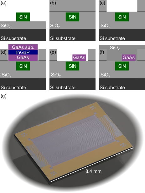
The devices are fabricated on Si wafers using LIGENTEC SiN PIC technology, outlined in Fig. 4. A SiN layer is deposited using low-pressure chemical vapor deposition (LPCVD) on top of a 4 m thick thermally oxidized Si layer. The SiN is patterned using deep-UV stepper photolithography to form waveguides using dry etching techniques. An SiO2 spacer layer is deposited with LPCVD and planarized using chemical mechanical polishing, leaving an 80 nm SiO2 spacer on top of the SiN waveguides. An etch-stop layer is used to preserve the thickness of the spacer layer in subsequent operations. A 2.7 m thick SiO2 layer is deposited forming the SiN top cladding. A window is etched through the top cladding to form the bonding area for the GaAs 80 nm above the SiN waveguides.
The GaAs waveguide layer is formed by directly bonding a GaAs chip to the SiO2 spacer layer. First, 5 nm of Al2O3 is deposited on the GaAs surface by atomic layer deposition to improve the bonding energy Sahoo et al. (2018); Zheng et al. (2018). Then, both bonding surfaces are cleaned and O2 plasma activated before bonding in atmosphere at room temperature. An anneal is performed at under pressure from a graphite fixture to strengthen the bond. The GaAs substrate is removed in two steps: first with mechanical lapping until 50 m remains, then a mixture of H2O2/NH4OH/H2O removes the remaining substrate, stopping on the InGaP layer. Previous work has used an Al0.8Ga0.2As layer for the etch-stop, which is removed with dilute HF Chang et al. (2018, 2019). However, the InGaP etch-stop layer used in this work is instead removed with HCl, which is more compatible with the current process since HCl does not etch the exposed SiO2. Next, the GaAs waveguide is patterned and etched with electron-beam lithography and ICP-RIE. A final PECVD SiO2 forms the top cladding. A metal layer is also fabricated on top of the SiO2 top cladding as part of this foundry process, but the metal layer is not used for this device.
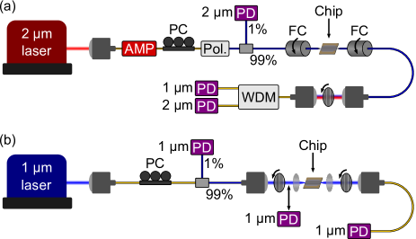
For the SHG experimental setup, shown in Fig. 5(a), a tunable 2 m wavelength laser is amplified. The polarization is adjusted to couple light to the slow-axis of the polarization maintaining (PM) fiber. A splitter taps 1 % of the input light to a photodetector to monitor the input power. Lensed PM fibers couple light into and out of the waveguides with the slow-axis aligned to the TE polarization. After the PM fiber, a free-space nanoparticle film polarizer is used to distinguish between TE and TM polarized light at the waveguide output. This polarizer has a transmission of 83 % and a polarization extinction ratio of 103 for both the 1 m and 2 m wavelengths. A broadband wavelength division multiplexer is used to separate the 1 m signal from the 2 m pump so both outputs can be monitored while the input wavelength is scanned.
Passive transmission measurements are performed using the setup shown in Fig. 5(b). Two different 1 m tunable lasers are used to cover wavelengths of 910–980 nm and 1045–1083 nm. The laser polarizations are aligned to the TM polarization of the waveguides. The input power is monitored on a photodetector from a 1 % power tap. Light is coupled on and off the chip in free-space using aspheric lenses and linear polarizers. The output light is fiber coupled and the power is monitored with a photodetector. Across a 100 nm bandwidth centered at 1 m, the polarization extinction ratio of the measurement setup is 103.
IV Experiment
SHG is demonstrated in both the reference device and the polarization rotator. The spectrum of the generated signal for each is shown in Fig. 6. After the signal is coupled to the output fiber, it passes through a linear polarizer aligned to the on-chip TE mode or TM mode to distinguish the power generated from each mode. The standard error of the signal power in each polarization is indicated with the shaded regions, as determined by polarization calibration measurements. Due to slight differences in the width of each waveguide (on the order of 5 nm), the phase matched pump wavelength of the reference device is 9 nm shorter than the polarization rotator device. At the peak of the reference signal, the light is % TM and % TE. As predicted, the polarization rotator device shows the opposite trend with an SHG signal at the peak of % TM and % TE light.
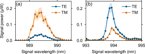
The SHG signal of the reference device in Fig. 6(a) has a full-width at half-max (FWHM) of 0.6 nm, which is wider than the FWHM from the polarization rotator device of 0.4 nm. This difference is not expected to be due to the different output couplers, but it is instead likely due to variations of the SHG waveguide width, thickness, or both. Similar observations have been made in our previous SHG experiments Chang et al. (2018). Notice that the reference device has a lower peak conversion efficiency due to greater index variations compared to the polarization rotator device. This also indicates that the insertion loss of the polarization rotator is similar to the insertion loss of the reference device.
Besides the efficient operation of the polarization rotator, both devices have lower SHG conversion efficiency than expected: 0.11 W-1 in this work compared to 2.50 W-1 from our previous work Chang et al. (2018). From transmission measurements, we found that the waveguide propagation loss is similar, on the order of 20 dB/cm near 1 m (due to surface-state absorption) and 0.5 dB/cm near 2 m. However, as we have noticed previously, there is an optimal length to achieve the maximum conversion efficiency. For short waveguides 2 mm, the conversion efficiency scales with the length squared, as expected from theoretical calculations. However, other mechanisms begin to degrade the efficiency as the length increases further, which we expect is due to propagation loss and variations in the effective indices of both the pump and signal modes due to geometric variations. These variations may be due to short-scale roughness at the interfaces between the waveguide core and cladding, but also larger-scale variations in the width and height of the waveguide due to lithography errors or an uneven termination after removing the etch-stop. Further investigation is required to fully understand the origin and magnitude of this degradation effect. One likely cause, as mentioned in Section III, is that a new etch-stop composed of InGaP was used in this work compared to the AlGaAs used in our previous work. The roughness on the top surface of the GaAs waveguide is 5.6 nm RMS, which contributes to phase decoherence. This roughness is likely inherent to the epitaxial wafer and we expect that the same etch-stop removal process will produce a more smooth waveguide surface when a new epitaxial wafer is used with a smooth interface between the GaAs waveguide layer and the InGaP etch-stop layer.
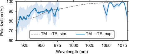
To understand the dependence of the polarization rotation on the signal wavelength, passive transmission measurements are performed with two different tunable lasers with wavelengths near 1 m. The polarization at the output of the polarization rotator is defined as . Light is input to the chip with a TM polarization and both TE and TM polarizations are measured separately at the output. These results are shown in Fig. 7 along with a grey dashed line indicating the simulated polarization trend. The measured polarization agrees well with the simulation, though small fluctuations on the order of 10 % are present due to Fabry-Perot resonances formed by reflections at the taper tips of the input SiN-GaAs coupler. While the simulation does not account for these reflections, other small fluctuations are also present in the simulated polarization trend that are not due to Fabry-Perot resonances. The physical effect that produces these fluctuations is the partial resonant coupling of the rotator. For wavelengths longer than 1075 nm, the coupling is accurately assumed to be purely adiabatic because the mode splitting, observed in Fig. 2(a), is sufficiently large. For the shorter wavelengths, the mode splitting is less significant, so a longer coupler would be necessary to achieve a purely adiabatic transition. The designed geometry achieves the largest mode-splitting and therefore most adiabatic transition permitted by other fabrication constraints.
V Conclusions
We have demonstrated a polarization rotator in a hybrid GaAs/SiN waveguide to couple light from a GaAs SHG waveguide to a SiN waveguide. The platform allows for the polarization rotator to have both vertical and horizontal asymmetry, which supports coupling between the fundamental TE and TM modes. SHG is demonstrated in this type I waveguide with a TE pump and a final TE signal at the output of the polarization rotator. The InGaP etch-stop process likely limits the conversion efficiency, and future work will minimize the roughness on the top surface of the GaAs waveguide. Polarization rotation is measured over a broad bandwidth, close to 100 nm, with excellent agreement to the design simulation. This device is suitable for integration with a SiN-based photonic integrated circuit to route and detect light for - self-referencing of an octave-spanning frequency comb.
Acknowledgements.
This work was funded by the DARPA MTO DODOS program. We thank Travis M. Autry, David R. Carlson, and Micheal Geiselmann for useful discussions and inputs on the manuscript.References
- Nicklaus et al. (2017) K. Nicklaus, M. Herding, A. Baatzsch, M. Dehne, C. Diekmann, K. Voss, F. Gilles, B. Guenther, B. Zender, S. Boehme, V. Mueller, D. Schuetze, G. Stede, B. Sheard, and G. Heinzel, “Optical bench of the laser ranging interferometer on GRACE Follow-On,” in International Conference on Space Optics–ICSO 2014, Vol. 10563 (International Society for Optics and Photonics, 2017) p. 105632I.
- Francis et al. (2018) S. P. Francis, T. T.-Y. Lam, D. E. McClelland, and D. A. Shaddock, “Multi-link laser interferometry architecture for interspacecraft displacement metrology,” J. Geod. 92, 241–251 (2018).
- Spencer et al. (2018) D. T. Spencer, T. Drake, T. C. Briles, J. Stone, L. C. Sinclair, C. Fredrick, Q. Li, D. Westly, B. R. Ilic, A. Bluestone, N. Volet, T. Komljenovic, L. Chang, S. H. Lee, D. Y. Oh, M.-G. Suh, K. Y. Yang, M. H. P. Pfeiffer, T. J. Kippenberg, E. Norberg, L. Theogarajan, K. Vahala, N. R. Newbury, K. Srinivasan, J. E. Bowers, S. A. Diddams, and S. B. Papp, “An optical-frequency synthesizer using integrated photonics,” Nature 557, 81–85 (2018).
- Newman et al. (2019) Z. L. Newman, V. Maurice, T. Drake, J. R. Stone, T. C. Briles, D. T. Spencer, C. Fredrick, Q. Li, D. Westly, B. R. Ilic, B. Shen, M.-G. Suh, K. Y. Yang, C. Johnson, D. M. S. Johnson, L. Hollberg, K. J. Vahala, K. Srinivasan, S. A. Diddams, J. Kitching, S. B. Papp, and M. T. Hummon, “Architecture for the photonic integration of an optical atomic clock,” Optica 6, 680–685 (2019).
- Malinowski et al. (2019) M. Malinowski, R. Bustos-Ramirez, J.-E. Tremblay, G. F. Camacho-Gonzalez, M. C. Wu, P. J. Delfyett, and S. Fathpour, “Towards On-Chip Self-Referenced Frequency-Comb Sources Based on Semiconductor Mode-Locked Lasers,” Micromachines 10, 391 (2019).
- Guo et al. (2017) X. Guo, C.-l. Zou, C. Schuck, H. Jung, R. Cheng, and H. X. Tang, “Parametric down-conversion photon-pair source on a nanophotonic chip,” Light: Sci. Appl. 6, e16249 (2017).
- Atzeni et al. (2018) S. Atzeni, A. S. Rab, G. Corrielli, E. Polino, M. Valeri, P. Mataloni, N. Spagnolo, A. Crespi, F. Sciarrino, and R. Osellame, “Integrated sources of entangled photons at the telecom wavelength in femtosecond-laser-written circuits,” Optica 5, 311–314 (2018).
- Singh et al. (2019) A. Singh, Q. Li, S. Liu, Y. Yu, X. Lu, C. Schneider, S. Höfling, J. Lawall, V. Verma, R. Mirin, S. W. Nam, J. Liu, and K. Srinivasan, “Quantum frequency conversion of a quantum dot single-photon source on a nanophotonic chip,” Optica 6, 563–569 (2019).
- Volet et al. (2018) N. Volet, X. Yi, Q.-F. Yang, E. J. Stanton, P. A. Morton, K. Y. Yang, K. J. Vahala, and J. E. Bowers, “Micro-resonator soliton generated directly with a diode laser,” Laser Photon. Rev. 12, 1700307 (2018).
- Suh et al. (2019) M.-G. Suh, C. Y. Wang, C. Johnson, and K. J. Vahala, “Directly pumped 10 GHz microcomb modules from low-power diode lasers,” Opt. Lett. 44, 1841–1843 (2019).
- Briles et al. (2018) T. C. Briles, J. R. Stone, T. E. Drake, D. T. Spencer, C. Fredrick, Q. Li, D. Westly, B. Ilic, K. Srinivasan, S. A. Diddams, and S. B. Papp, “Interlocking Kerr-microresonator frequency combs for microwave to optical synthesis,” Opt. Lett. 43, 2933–2936 (2018).
- Gaeta, Lipson, and Kippenberg (2019) A. L. Gaeta, M. Lipson, and T. J. Kippenberg, “Photonic-chip-based frequency combs,” Nat. Photon. 13, 158 (2019).
- Huang et al. (2019) D. Huang, M. A. Tran, J. Guo, J. Peters, T. Komljenovic, A. Malik, P. A. Morton, and J. E. Bowers, “High-power sub-kHz linewidth lasers fully integrated on silicon,” Optica 6, 745–752 (2019).
- Chang et al. (2018) L. Chang, A. Boes, X. Guo, D. T. Spencer, M. J. Kennedy, J. D. Peters, N. Volet, J. Chiles, A. Kowligy, N. Nader, D. D. Hickstein, E. J. Stanton, S. A. Diddams, S. B. Papp, and J. E. Bowers, “Heterogeneously integrated GaAs waveguides on insulator for efficient frequency conversion,” Laser Photon. Rev. 12, 1800149 (2018).
- Chang et al. (2019) L. Chang, A. Boes, P. Pintus, J. D. Peters, M. J. Kennedy, X.-W. Guo, N. Volet, S.-P. Yu, S. B. Papp, and J. E. Bowers, “Strong frequency conversion in heterogeneously integrated GaAs resonators,” APL Photonics 4, 036103 (2019).
- Stanton et al. (2019) E. J. Stanton, J. Chiles, N. Nader, S. W. Nam, and R. P. Mirin, “Wafer-scale GaAs-on-insulator waveguide platform for diverse nonlinear processes,” in CLEO: Science and Innovations (Optical Society of America, 2019) pp. SM3O–5.
- May et al. (2019) S. May, M. Kues, M. Clerici, and M. Sorel, “Second-harmonic generation in AlGaAs-on-insulator waveguides,” Opt. Lett. 44, 1339–1342 (2019).
- Fiore et al. (1998a) A. Fiore, V. Berger, E. Rosencher, P. Bravetti, and J. Nagle, “Phase matching using an isotropic nonlinear optical material,” Nature 391, 463 (1998a).
- Fiore et al. (1998b) A. Fiore, S. Janz, L. Delobel, P. Van der Meer, P. Bravetti, V. Berger, E. Rosencher, and J. Nagle, “Second-harmonic generation at =1.6 m in AlGaAs/Al2O3 waveguides using birefringence phase matching,” Appl. Phys. Lett. 72, 2942–2944 (1998b).
- Wang et al. (2018) C. Wang, C. Langrock, A. Marandi, M. Jankowski, M. Zhang, B. Desiatov, M. M. Fejer, and M. Lončar, “Ultrahigh-efficiency wavelength conversion in nanophotonic periodically poled lithium niobate waveguides,” Optica 5, 1438–1441 (2018).
- Desiatov et al. (2019) B. Desiatov, A. Shams-Ansari, M. Zhang, C. Wang, and M. Lončar, “Ultra-low-loss integrated visible photonics using thin-film lithium niobate,” Optica 6, 380–384 (2019).
- Pu et al. (2016) M. Pu, L. Ottaviano, E. Semenova, and K. Yvind, “Efficient frequency comb generation in AlGaAs-on-insulator,” Optica 3, 823–826 (2016).
- Liu et al. (2019) Y. Liu, M. Galili, K. Yvind, L. K. Oxenløwe, H. Hu, and M. Pu, “High-Order Phase-Matching Enabled Octave-Bandwidth Four-Wave Mixing in AlGaAs-On-Insulator Waveguides,” in CLEO: Applications and Technology (Optical Society of America, 2019) pp. JTu2A–83.
- Zheng et al. (2018) Y. Zheng, M. Pu, H. K. Sahoo, E. Semenova, and K. Yvind, “High-Quality-Factor AlGaAs-on-Sapphire Microring Resonators,” J. Lightw. Technol. 37, 868–874 (2018).
- Chiles et al. (2019) J. Chiles, N. Nader, E. J. Stanton, D. Herman, G. Moody, J. Zhu, J. C. Skehan, B. Guha, A. Kowligy, J. T. Gopinath, K. Srinivasan, S. A. Diddams, I. Coddington, N. R. Newbury, J. M. Shainline, S. W. Nam, and R. P. Mirin, “Multi-functional integrated photonics in the mid-infrared with suspended AlGaAs on silicon,” arXiv preprint arXiv:1905.01380 (2019).
- Skauli et al. (2002) T. Skauli, K. L. Vodopyanov, T. J. Pinguet, A. Schober, O. Levi, L. A. Eyres, M. M. Fejer, J. S. Harris, B. Gerard, L. Becouarn, E. Lallier, and G. Arisholm, “Measurement of the nonlinear coefficient of orientation-patterned GaAs and demonstration of highly efficient second-harmonic generation,” Opt. Lett. 27, 628–630 (2002).
- Wang and Dai (2008) Z. Wang and D. Dai, “Ultrasmall Si-nanowire-based polarization rotator,” J. Opt. Soc. Am. B 25, 747–753 (2008).
- Dai and Bowers (2011) D. Dai and J. E. Bowers, “Novel concept for ultracompact polarization splitter-rotator based on silicon nanowires,” Opt. Express 19, 10940–10949 (2011).
- Obayya et al. (2001) S. Obayya, B. Rahman, K. Grattan, and H. El-Mikati, “Beam propagation modeling of polarization rotation in deeply etched semiconductor bent waveguides,” IEEE Photon. Technol. Lett. 13, 681–683 (2001).
- Sacher et al. (2014) W. D. Sacher, T. Barwicz, B. J. F. Taylor, and J. K. S. Poon, “Polarization rotator-splitters in standard active silicon photonics platforms,” Opt. Express 22, 3777–3786 (2014).
- Sahoo et al. (2018) H. K. Sahoo, L. Ottaviano, Y. Zheng, O. Hansen, and K. Yvind, “Low temperature bonding of heterogeneous materials using Al2O3 as an intermediate layer,” J. Vac. Sci. Technol. B 36, 011202 (2018).