Group III Quantum Defects in Diamond are Stable Spin-1 Color Centers
Abstract
Color centers in diamond have emerged as leading solid-state “artificial atoms” for a range of quantum technologies, from quantum sensing to quantum networks. Concerted research activities are now underway to identify new color centers that combine stable spin and optical properties of the nitrogen vacancy (NV–) with the spectral stability of the silicon vacancy (SiV–) centers in diamond, with recent research identifying other group IV color centers with superior properties. In this Letter, we investigate a new class of diamond quantum emitters from first principles, the group III color centers, which we show to be thermodynamically stable in a spin-1, electric-field insensitive structure. From ab initio electronic structure methods, we characterize the product Jahn-Teller (pJT) effect present in the excited state manifold of these group III color centers, where we capture symmetry-breaking distortions associated with strong electron-phonon coupling. These predictions can guide experimental identification of group III vacancy centers and their use in applications in quantum information science and technology.
Diamond color centers are promising building blocks for applications such as quantum sensing and quantum communication,Jelezko and Wrachtrup (2006); Weber et al. (2010); Aharonovich et al. (2016); Awschalom et al. (2018) such as in the recent demonstration of the generation of entanglement between two distant diamond nitrogen vacancy (NV–) centers at a rate faster than their decoherenceHumphreys et al. (2018). While this result marks a major milestone towards the development of scalable quantum networks, the entanglement generation rate could be improved by orders of magnitude with a high-efficiency photonic interface to the emitter’s coherent optical transition. One route is to couple the NV–center to a micro- or nano-cavity to enhance spontaneous emission into the coherent zero phonon line, but more work is needed to overcome the NV–’s spectral diffusion near surfaces Atatüre et al. (2018), which arises primarily from its C3v symmetry, giving rise to a permanent electric dipole moment.
Another approach, which is considered here, is to develop alternative color centers that have stable optical and spin properties. Within the diamond material system, the group IV vacancy centers (SiV–, GeV–, SnV–, and PbV–) have been characterized experimentally Neu et al. (2013); Inubushi et al. (2015); Siyushev et al. (2017); Trusheim et al. (2019) and theoretically Thiering and Gali (2018); Gali and Maze (2013); Thiering and Gali (2019). The group IV negative centers adopt an inversion-symmetric split-vacancy structure which has no permanent electric dipole moment, making their optical transitions less sensitive to electric field noise near surfaces Sipahigil et al. (2014). Additionally, the branching ratio into the zero phonon line (ZPL) can be more than an order of magnitude higher than for the NV center, though this gain is partially offset by a lower internal quantum efficiency. Unfortunately, the negatively charged group IV centers suffer from a phonon-mediated dephasing mechanism of the ground state spin structure, which limits their spin coherence times Doherty et al. (2015). Recent findings suggest that by careful boron doping of diamond, the SiV can favor a neutral charge with the stable spin-1 electronic ground state of the NV– center and the stable optical transitions of the SiV– Rose et al. (2018), though more work is needed to demonstrate both properties in the same emitter. A natural question is whether there are other color centers that exhibit stable optical and spin properties in their thermodynamically favored charge state in intrinsic diamond. Outside of the group IV centers, previous work has characterized other dopant-vacancy centers in diamond Goss et al. (2005); however their optoelectronic properties are not yet understood.
In this Letter, we report predictions of the diamond group III vacancy defects XV, with X = Al, Ga, In, and Tl, and characterize their properties using ab initio electronic structure theory of the ground and excited state manifolds. Our calculations reveal that the three lightest defects are stable in the high-symmetry D3d configuration, with a thermodynamically preferred –1 charge state which makes them isoelectronic with the SiV0 defect. We characterize the product Jahn-Teller (pJT) effect Qiu and Ceulemans (2001); Thiering and Gali (2019) present in the excited state manifold, where we capture symmetry-breaking distortions associated with strong electron-phonon coupling. We discuss the impact of these distortions, in particular on the predicted zero-phonon line energies. We also capture vibronic spectra and discuss the relatively high predicted ZPL emission efficiency found. Overall, the group III vacancy centers are found to be similar to their group IV neutral counterparts, but with a spin-1 ground state for the thermodynamically stable negative charge state in intrinsic diamond. The combination of the stable spin-1 ground state and symmetry-protected optical transitions makes these centers excellent candidates for quantum technologies.
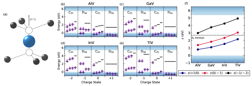
First, we investigate the electronic properties of the group III vacancies for aluminum, gallium, indium, and thallium using density functional theory with the HSE06 hybrid functional Giannozzi et al. (2009, 2017); Schlipf and Gygi (2015a); Heyd et al. (2003, 2006). All four centers are found to be stable in the split-vacancy configuration shown in Fig. 1(a). Depending on the charge state, this configuration has either a D3d geometry with the principal axis oriented along the [111] crystallographic direction, or a C2h geometry. Both configurations are inversion symmetric about the substituent atom, and therefore cannot have a net dipole moment, making their optical transitions insensitive to charge noise. Each of the presented calculations uses a 512 atom ‘supercell’ and samples the point; we refer to the SI for computational details and convergence studies.
As previous work Hepp et al. (2014); Gali and Maze (2013); Thiering and Gali (2018, 2019) has established for group IV emitters in diamond, the orbitals associated with the group III defects can be identified by their symmetry. Two pairs of degenerate Kohn-Sham (KS) orbitals are localized within the diamond bandgap, having and symmetry, respectively. The orbitals within each degenerate pair are denoted as and , where or refers to their orientation. While additional localized defect orbitals are present, they are energetically far from the band edges and are therefore not accessible for optical excitation.
Figure 1 shows the electronic ground state configurations for these defects in charge states from –2 to +1. Panels (b-e) plot the energies of the spin majority (spin up) and spin minority (spin down) channels for each of the defects, where the orbitals lie below the orbitals in each case.
Of particular interest are the –1 charge states, which are spin-1 states, isoelectronic to the group IV neutrals Thiering and Gali (2019) and stable in a D3d configuration. For each defect, the ground state electronic configuration of the –1 charge state is denoted by , such that there are two unfilled orbitals, both of the same spin channel. This can equivalently be formulated in terms of a pair of holes occupying the remaining ground state orbitals. In contrast to ab initio orbital energetics of group IV neutral systems Thiering and Gali (2018, 2019), where the KS orbitals lie below the valence band edge, both the and levels for the spin-minority channel are located within the band gap for the group III negatives. This difference could lead to improved excitation efficiency for the group III vacancy centers, as these defect-defect transitions are energetically isolated from any bulk states.
Next, we calculate which charge state is thermodynamically most favorable at a given doping level for the diamond host. The Fermi level at which a transition becomes thermodynamically stable is given by the charge transition levels: Freysoldt et al. (2014)
| (1) |
with being the total energy from the supercell calculation in charge state , and the corresponding charge correction to account for periodic interaction of charges between neighboring supercells Sundararaman and Ping (2017); Freysoldt et al. (2009). We apply the correction techniques described in Ref. 26, yielding the results summarized in Fig. 1(f).
For aluminum, gallium, and indium substituents, the intrinsic Fermi level lies between the transition energies and , indicating that the –1 charge state is thermodynamically stable in intrinsic diamond. Following a similar trend to the group IV elements Thiering and Gali (2018), the transition energies are higher for the heavier elements, resulting in the neutral charge state being favored for thallium. This neutral charge state is spin ½ and relaxes into a C2h symmetry due to its uneven orbital occupation (i.e. it is Jahn-Teller unstable). The moderate nitrogen doping typically present in diamond samples means that we might still expect to see the desirable –1 charge state in as-grown diamond for TlV, since the transition lies close to the intrinsic Fermi level.
Given that these color centers are isoelectronic with the SiV0, the negatively charged group III vacancy centers are expected to have similar electronic properties to the SiV0 in the ground and excited states. In particular, exciting an electron from the lower-energy to the higher energy orbital means that the electronic configuration becomes , producing an unequal occupation of the two degenerate orbital pairs. Such a system is expected to be Jahn-Teller unstable Schmidtke (1990) as a result of a product of two the Jahn-Teller instabilities for both the and orbitals, denoted as a product Jahn-Teller effect Thiering and Gali (2019). Here is the irreducible representation of the coupled phonon modes that produce the distortion. Each of these modes is two-fold degenerate, and the Jahn-Teller distortion therefore resides in a two-dimensional coordinate space that contains the high-symmetry D3d point, as well as three equivalent energy minima in the C2h symmetry group. Accurately capturing the Jahn-Teller effect is important in predicting the experimentally relevant zero phonon line energy associated with optical emission, as the pJT symmetry reduction can result in a large energy change in the excited state, as seen in the case of the SiV0 Green et al. (2019); Rose et al. (2018); Thiering and Gali (2019).
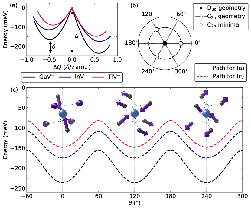
To capture this effect in group III vacancy centers, we relax the GaV–, InV–, and TlV– defects in the excited electronic state using constrained DFT (SCF) within Quantum Espresso Giannozzi et al. (2009, 2017) with norm-conserving pseudopotentials Schlipf and Gygi (2015b) in a plane-wave basis with energy cutoff of 80 Ry. First, we relax the system constrained to both a D3d and a C2h geometry with excited electronic occupations until forces on all atoms are below Ry/Bohr. We additionally verify that the resulting C2h structure is the true minimum of the excited state manifold by relaxing without any symmetry constraints. From these relaxed C2h and D3d geometries, we can construct the full potential energy surface associated with the Jahn-Teller modes in the excited manifold. While the AlV– is not explicitly discussed next, it is expected to follow the same trends as the heavier group III elements.
Similar to the behavior of the group IV neutral excited states in Ref. 13, there may exist four distinct excited states depending on the occupations of the defect orbitals, as can be seen from the fact that there are two holes that can occupy two orbitals. However, constrained DFT is only able to access the lowest energy for a given constrained configuration, and we therefore consider only the lowest-energy configurations of the excited state manifold for a particular geometry. Future extensions of this work could use a formalism along the lines of Refs. 31; 32 which restrict the symmetry of the orbitals, allowing for a better approximation of the many-body Hamiltonian and a slightly more accurate ZPL energy calculation. Nevertheless, the information at hand allows us to calculate ZPL energies, optical spectra, and Debye-Waller factors while neglecting the relatively small many-body effects. The calculated ZPL energies, given as the energy difference between the the C2h excited electronic state and the D3d ground electronic state, are summarized in Table 1.
Figure 2 and Table 1 summarize the results of the pJT calculations. Panel (a) shows a one-dimensional interpolation of the excited-state potential energy surface between the D3d (located at ) and C2h geometries. The global minimum is the relaxed C2h geometry, while the local minimum on the opposite side of the D3d point is a saddle point. The energy differences between the D3d and global C2h minima () and the saddle point and global C2h minima () are presented in Table 1. In the first-order Jahn-Teller effect, the potential energy surface would be symmetrical with respect to the D3d point, such that . However, given the relatively large values of , higher order effects are clearly important in this system Schmidtke (1990).
In Fig. 2(c), we map out the energy of the system along a circle through the Jahn-Teller coordinate space which traverses the three energetically equivalent C2h minimum geometries, as well as the energy barriers between them caused by the higher-order Jahn-Teller coupling. The trajectories in the coordinate space shown in Fig. 2(a,c) are visualized in Fig. 2(b), where we depict the locations of high-symmetry D3d geometry along with the three equivalent C2h configurations within the JT space. The movement of the nearest neighbor carbons resulting from each of the equivalent distortions are shown as well. We note that each distortion affects one pair of the nearby carbon atoms more than the other two. By adding each of these distortions together, we arrive at the high symmetry D3d geometry once again.
| (meV) | (meV) | (nm, eV) | |
|---|---|---|---|
| GaV– | 236 | 71 | 679, 1.82 |
| InV– | 175 | 60 | 584, 2.12 |
| TlV– | 148 | 58 | 437, 2.84 |
To characterize the optical properties, we calculate ab initio emission lineshapes using the method outlined in Ref. 33. Phonon properties for the ground state geometries of each of the –1 charge state defects were evaluated using a computationally more efficient PBE functional Garrity et al. (2014); Perdew et al. (1996); Togo and Tanaka (2015), which has previously been found to be sufficiently accurate compared to the hybrid functionals used earlier Hummer et al. (2009). The emission lineshape can then be calculated from the overlap of the ionic vibrational wavefunctions between the relaxed excited electronic state and the electronic ground vibrational states Alkauskas et al. (2012, 2014) according to
| (2) |
where is the th vibrational state of the ground (excited) electronic state and is the frequency of the transition. represents the energy of the vibrational state . The true emission lineshape is determined by Fermi’s golden rule, and is proportional to this overlap and the transition frequency as .
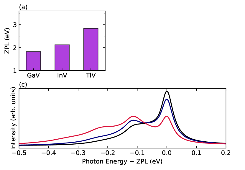
The vibrational overlaps are evaluated using a generating function approach as described previously Alkauskas et al. (2014). The generating function method assumes that the modes in the ground and excited state are identical, and there is only a difference in geometry between the two configurations. This assumption is strongly violated when a Jahn-Teller distortion occurs in the excited state, since the symmetries between the two geometries are different. Using the transition therefore underestimates the overlap of the ground vibrational states in the ground and excited state electronic manifolds. Previous theoretical approaches for generating emission spectra for JT-unstable defects in diamond have neglected the effect of the JT distortion by equally occupying the degenerate electronic orbitals using fractional occupations, effectively enforcing a high-symmetry configurations (e.g., in the NV– Alkauskas et al. (2014) and SiV– Londero et al. (2018)). We use a similar approximation by studying the phonon coupling to the emission from the excited state with the correct orbital occupations, but restricted to a D3d geometry. We note that this leads to a slightly lower Debye-Waller factor than the fractional occupation technique for the excited electronic states.
The lineshapes give information on what to expect from photoluminescence experiments. The Debye-Waller factor, which describes the overall emission efficiency into the ZPL, is an important figure of merit for the performance of these defects in quantum protocols such as photon-mediated entanglement Aharonovich et al. (2016). The resulting spectra, along with the predicted Huang-Rhys and Debye-Waller factors, are given in Fig. 3. The emission efficiency into the ZPL is much higher than what is observed in NV– Doherty et al. (2013), although we find that the efficiency decreases for heavier defect elements.
In conclusion, we predict the quantum optoelectronic properties of diamond group III vacancy centers. Our calculations show that these color centers are stable in intrinsic diamond in a spin state with a symmetry that makes their transitions insensitive to electric fields. The combination of favorable thermodynamics, stable spin, and symmetry-protected optical properties makes the negatively charged group III vacancy centers ideal candidates for applications such as quantum networking and computing. The emerging ability to perform detailed calculations on spin and optical properties of nanoscopic quantum emitters, including corrections such as the large product Jahn-Teller effect, marks an important step towards ab initio design and discovery of quantum materials. In particular, the predicted properties of the group III vacancy class of emitters would combine the desired attributes of high Debye-Waller factors with highly coherent spin and optical transitions at a range of wavelengths, promising a new class of quantum emitters for applications in quantum information science and technology.
Acknowledgments
We thank Dr. Matthew Trusheim (MIT-Harvard) for helpful discussions. This work was supported by the DOE ‘Photonics at Thermodynamic Limits’ Energy Frontier Research Center under grant number DE-SC0019140. D. E. and P.N. are partially supported by the Army Research Office MURI (Ab-Initio Solid-State Quantum Materials) grant number W911NF-18-1-0431. J.F. acknowledges fellowship support from the Deutsche Forschungsgemeinschaft (DFG) under Contract No. FL 997/1-1. P.N. is a Moore Inventor Fellow and a CIFAR Azrieli Global Scholar.
Calculations were performed using resources from the Department of Defense High Performance Computing Modernization program. Additional calculations were performed using resources of the National Energy Research Scientific Computing Center, a DOE Office of Science User Facility, as well as resources at the Research Computing Group at Harvard University.
References
- Jelezko and Wrachtrup (2006) F. Jelezko and J. Wrachtrup, Physica Status Solidi (A) Applications and Materials Science 203, 3207 (2006), 0307085 [cond-mat] .
- Weber et al. (2010) J. R. Weber, W. F. Koehl, J. B. Varley, A. Janotti, B. B. Buckley, C. G. Van de Walle, and D. D. Awschalom, Proceedings of the National Academy of Sciences of the United States of America 107, 8513 (2010).
- Aharonovich et al. (2016) I. Aharonovich, D. Englund, and M. Toth, Nature Photonics 10, 631 EP (2016).
- Awschalom et al. (2018) D. D. Awschalom, R. Hanson, J. Wrachtrup, and B. B. Zhou, Nature Photonics 12, 516 (2018).
- Humphreys et al. (2018) P. C. Humphreys, N. Kalb, J. P. J. Morits, R. N. Schouten, R. F. L. Vermeulen, D. J. Twitchen, M. Markham, and R. Hanson, Nature 558, 268 (2018).
- Atatüre et al. (2018) M. Atatüre, D. Englund, N. Vamivakas, S.-Y. Lee, and J. Wrachtrup, Nature Reviews Materials 3, 38 (2018).
- Neu et al. (2013) E. Neu, C. Hepp, M. Hauschild, S. Gsell, M. Fischer, H. Sternschulte, Doris Steinmüller-Nethl, M. Schreck, and C. Becher, New Journal of Physics 15, 43005 (2013).
- Inubushi et al. (2015) T. Inubushi, N. Mizuochi, F. Ishibashi, M. Hatano, Y. Doi, Y. Miyamoto, L. J. Rogers, S. Kobayashi, S. Yamasaki, F. Jelezko, S. Nagamachi, B. Naydenov, K. Tahara, K. D. Jahnke, T. Iwasaki, and T. Miyazaki, Scientific Reports 5, 12882 (2015).
- Siyushev et al. (2017) P. Siyushev, M. H. Metsch, T. Iwasaki, Y. Miyamoto, F. Jelezko, T. Taniguchi, and M. Hatano, Physical Review Letters 119, 253601 (2017).
- Trusheim et al. (2019) M. E. Trusheim, N. H. Wan, K. C. Chen, C. J. Ciccarino, J. Flick, R. Sundararaman, G. Malladi, E. Bersin, M. Walsh, B. Lienhard, H. Bakhru, P. Narang, and D. Englund, Physical Review B 99, 075430 (2019).
- Thiering and Gali (2018) G. Thiering and A. Gali, Physical Review X 8 (2018), 10.1103/PhysRevX.8.021063.
- Gali and Maze (2013) A. Gali and J. R. Maze, Physical Review B 88 (2013), 10.1103/PhysRevB.88.235205.
- Thiering and Gali (2019) G. Thiering and A. Gali, npj Computational Materials 5, 18 (2019).
- Sipahigil et al. (2014) A. Sipahigil, K. D. Jahnke, L. J. Rogers, T. Teraji, J. Isoya, A. S. Zibrov, F. Jelezko, and M. D. Lukin, Physical Review Letters 113, 113602 (2014), 1406.4268 .
- Doherty et al. (2015) M. W. Doherty, M. Metsch, N. B. Manson, M. D. Lukin, F. Jelezko, A. Sipahigil, K. D. Jahnke, L. J. Rogers, and J. M. Binder, New Journal of Physics 17, 043011 (2015).
- Rose et al. (2018) B. C. Rose, D. Huang, Z.-H. Zhang, P. Stevenson, A. M. Tyryshkin, S. Sangtawesin, S. Srinivasan, L. Loudin, M. L. Markham, A. M. Edmonds, D. J. Twitchen, S. A. Lyon, and N. P. de Leon, Science 361, 60 (2018).
- Goss et al. (2005) J. P. Goss, P. R. Briddon, M. J. Rayson, S. J. Sque, and R. Jones, Physical Review B 72, 035214 (2005).
- Qiu and Ceulemans (2001) Q. C. Qiu and A. Ceulemans, “The vibronic coupling case: A prototypal product jahn-teller system,” in Vibronic Interactions: Jahn-Teller Effect in Crystals and Molecules, edited by M. D. Kaplan and G. O. Zimmerman (Springer Netherlands, Dordrecht, 2001) pp. 97–102.
- Giannozzi et al. (2009) P. Giannozzi, S. Baroni, N. Bonini, M. Calandra, R. Car, C. Cavazzoni, Davide Ceresoli, G. L. Chiarotti, M. Cococcioni, I. Dabo, A. D. Corso, S. de Gironcoli, S. Fabris, G. Fratesi, R. Gebauer, U. Gerstmann, C. Gougoussis, A. Kokalj, M. Lazzeri, L. Martin-Samos, N. Marzari, F. Mauri, R. Mazzarello, Stefano Paolini, A. Pasquarello, L. Paulatto, C. Sbraccia, S. Scandolo, G. Sclauzero, A. P. Seitsonen, A. Smogunov, P. Umari, and R. M. Wentzcovitch, Journal of Physics: Condensed Matter 21, 395502 (2009).
- Giannozzi et al. (2017) P. Giannozzi, O. Andreussi, T. Brumme, O. Bunau, M. B. Nardelli, M. Calandra, R. Car, C. Cavazzoni, D Ceresoli, M. Cococcioni, N. Colonna, I. Carnimeo, A. D. Corso, S. de Gironcoli, P. Delugas, R. A. D. Jr, A Ferretti, A. Floris, G. Fratesi, G. Fugallo, R. Gebauer, U. Gerstmann, F. Giustino, T. Gorni, J. Jia, M. Kawamura, H-Y Ko, A. Kokalj, E. Küçükbenli, M. Lazzeri, M. Marsili, N. Marzari, F. Mauri, N. L. Nguyen, H.-V. Nguyen, A Otero-de-la-Roza, L. Paulatto, S. Poncé, D. Rocca, R. Sabatini, B. Santra, M. Schlipf, A. P. Seitsonen, A. Smogunov, I Timrov, T. Thonhauser, P. Umari, N. Vast, X. Wu, and S. Baroni, Journal of Physics: Condensed Matter 29, 465901 (2017).
- Schlipf and Gygi (2015a) M. Schlipf and F. Gygi, Computer Physics Communications 196, 36 (2015a).
- Heyd et al. (2003) J. Heyd, G. E. Scuseria, and M. Ernzerhof, Journal of Chemical Physics 118, 8207 (2003).
- Heyd et al. (2006) J. Heyd, G. E. Scuseria, and M. Ernzerhof, The Journal of Chemical Physics 124, 219906 (2006).
- Hepp et al. (2014) C. Hepp, T. Müller, V. Waselowski, J. N. Becker, B. Pingault, H. Sternschulte, D. Steinmüller-Nethl, A. Gali, J. R. Maze, M. Atatüre, and C. Becher, Physical Review Letters 112, 036405 (2014), 1310.3106 .
- Freysoldt et al. (2014) C. Freysoldt, B. Grabowski, T. Hickel, J. Neugebauer, G. Kresse, A. Janotti, and C. G. de Walle, Reviews of Modern Physics 86, 253 (2014).
- Sundararaman and Ping (2017) R. Sundararaman and Y. Ping, The Journal of Chemical Physics 146, 104109 (2017).
- Freysoldt et al. (2009) C. Freysoldt, J. Neugebauer, and C. G. de Walle, Physical Review Letters 102, 16402 (2009).
- Schmidtke (1990) H.-H. Schmidtke, Berichte der Bunsengesellschaft für physikalische Chemie 94, 896 (1990).
- Green et al. (2019) B. L. Green, M. W. Doherty, E. Nako, N. B. Manson, U. F. S. D’Haenens-Johansson, S. D. Williams, D. J. Twitchen, and M. E. Newton, Phys. Rev. B 99, 161112 (2019).
- Schlipf and Gygi (2015b) M. Schlipf and F. Gygi, Computer Physics Communications 196, 36 (2015b).
- Kaduk et al. (2012) B. Kaduk, T. Kowalczyk, and T. Van Voorhis, Chemical Reviews 112, 321 (2012), pMID: 22077560, https://doi.org/10.1021/cr200148b .
- Plaisance et al. (2017) C. P. Plaisance, R. A. van Santen, and K. Reuter, Journal of Chemical Theory and Computation 13, 3561 (2017), pMID: 28657733, https://doi.org/10.1021/acs.jctc.7b00362 .
- Alkauskas et al. (2014) A. Alkauskas, B. B. Buckley, D. D. Awschalom, and C. G. Van De Walle, New Journal of Physics 16, 073026 (2014).
- Garrity et al. (2014) K. F. Garrity, J. W. Bennett, K. M. Rabe, and D. Vanderbilt, Comp. Mat. Sci. 81, 446 (2014).
- Perdew et al. (1996) J. P. Perdew, K. Burke, and M. Ernzerhof, Phys. Rev. Lett. 77, 3865 (1996).
- Togo and Tanaka (2015) A. Togo and I. Tanaka, Scripta Materialia 108, 1 (2015), 1506.08498 .
- Hummer et al. (2009) K. Hummer, J. Harl, and G. Kresse, Phys. Rev. B 80, 115205 (2009).
- Alkauskas et al. (2012) A. Alkauskas, J. L. Lyons, D. Steiauf, and C. G. de Walle, Physical Review Letters 109, 267401 (2012).
- Londero et al. (2018) E. Londero, G. Thiering, L. Razinkovas, A. Gali, and A. Alkauskas, Physical Review B 98, 035306 (2018).
- Doherty et al. (2013) M. W. Doherty, N. B. Manson, P. Delaney, F. Jelezko, J. Wrachtrup, and L. C. L. Hollenberg, Physics Reports 528, 1 (2013).