Magneto-ionic control of spin polarization in magnetic tunnel junctions
Abstract
Magnetic tunnel junctions (MTJs) with Hf0.5Zr0.5O2 barriers are reported to show both tunneling magnetoresistance effect (TMR) and tunneling electroresistance effect (TER), displaying four resistance states by magnetic and electric field switching. Here we show that, under electric field cycling of large enough magnitude, the TER can reach values as large as 106%. Moreover, concomitant with this TER enhancement, the devices develop electrical control of spin polarization, with sign reversal of the TMR effect. Currently, this intermediate state exists for a limited number of cycles and understanding the origin of these phenomena is key to improve its stability. The experiments presented here point to the magneto-ionic effect as the origin of the large TER and strong magneto-electric coupling, showing that ferroelectric polarization switching of the tunnel barrier is not the main contribution.
Combining the TMR effect of magnetic tunnel junctions (MTJs) with additional functionalities provided by the tunnel barrier, i.e. using multiferroicGajek et al. (2007) or ferroelectricRodrıguez Contreras et al. (2003); Tsymbal et al. (2012) layers as barriers, has drawn considerable attention driven by their potential application in multilevel memories. In these devices, four resistance states are achieved by means of both the TMR (resistance change induced by magnetic field switching) and the TER (resistance change by electric switching) effects.Scott (2007); Hur et al. (2004); Bibes and Barthélémy (2008) In addition, by combining two ferroic orders (ferromagnetic and ferroelectric), the coupling between the magnetic and electric degrees of freedom could realize electric field controlled spintronics, promising for the development of low-power and fast devices.Ortega et al. (2015); Webster (2002); Eerenstein, Mathur, and Scott (2006); Ramesh and Spaldin (2007); Fiebig (2005); Garcia et al. (2010); Yin and Li (2017); Bibes and Barthélémy (2008)
Four main types of magnetoelectric (ME) coupling mechanismsDong, Xiang, and Dagotto (2019); Dong et al. (2015); Bauer et al. (2015) are established. Firstly, spin-orbit coupling, which can directly link the breaking of space and time inversion symmetry (charge dipoles and magnetic moments).Eerenstein, Mathur, and Scott (2006) Secondly, spin-lattice coupling,Lee et al. (2010); Fabrèges et al. (2009) that profits from the piezoelectric properties of ferroelectrics and the magnetostrictive properties of ferromagnets. In this case strain can couple electric field with magnetization or magnetic field with electrical polarization.Tsymbal and Kohlstedt (2006); Gajek et al. (2007) Thirdly, the ME coupling can originate from spin-charge coupling mediated by the carrier density.Rondinelli, Stengel, and Spaldin (2008) At the interface between an insulator and a ferromagnetic metal, accumulation of spin-polarized carriers and, thus magnetization, is expected upon application of an electric field that leads to polarization of the dielectric. This effect is enhanced in the case of a polar barrier, as a larger number of carriers is necessary for screening. Finally, the magneto-ionic effectBauer et al. (2015) has been recently proposed, by which the applied electric field induces ion migration that modifies the interfaces of the ferromagnetic layers involved in the junctions. All these mechanisms could contribute to the ME coupling, separately or jointly.
In this work, tunnel barriers of crystalline Hf0.5Zr0.5O2 (HZO) are used in MTJs. Crystalline HZO grown under certain conditions has shown nanoscale ferroelectricity.Böscke et al. (2011); Park et al. (2015). Epitaxial growth of crystalline HZO can also be achievedShimizu et al. (2016) and has been recently also demonstrated on perovskite substrates with La0.7Sr0.3MnO3 (LSMO) as bottom elecrodeWei et al. (2018); Lyu et al. (2018, 2019). Four resistance states have been obtained in this type of junctions by both magnetic and electric field switching, but no ME coupling was reported.Wei et al. (2019) Here we show that electric field cycling induces irreversible changes in the junction, which evolves from a negligible ME coupling state into a large ME coupling state. In the latter, sign reversal of the TMR effect is achieved by electrical switching reversibly. Concomitantly, with increasing number of cycles, the TER increases to values up to 106%. In the following we discuss the mechanisms that lead to such phenomena.
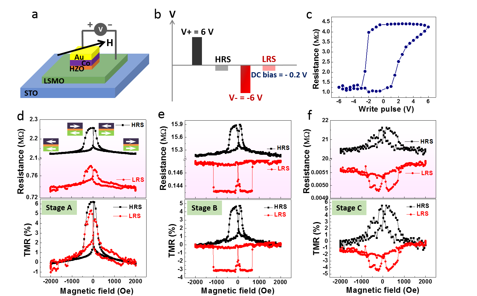
MTJs have been fabricated by integrating 2 nm HZO tunnel barriers between top Co and bottom La0.7Sr0.3MnO3 (LSMO) ferromagnetic (FM) electrodes. The HZO is highly crystalline and epitaxially grown on the LSMO electrode, which is in turn epitaxially grown on 001-oriented SrTiO3 (STO) substrates. As reported in ref.Wei et al. (2019), the large band gap and high resistance of the HZO layer allows to fabricate full devices with extended electrodes for wire bonding, despite the low thickness of the barrier. This is not possible with perovskite ferroelectric (FE) tunnel barriers with such small thickness and, thus, so far these devices have been limited to investigation by scanning probes. The schematic drawing of the devices used in the present work is shown in Fig. 1a. (See details in methods section).
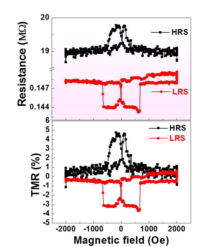
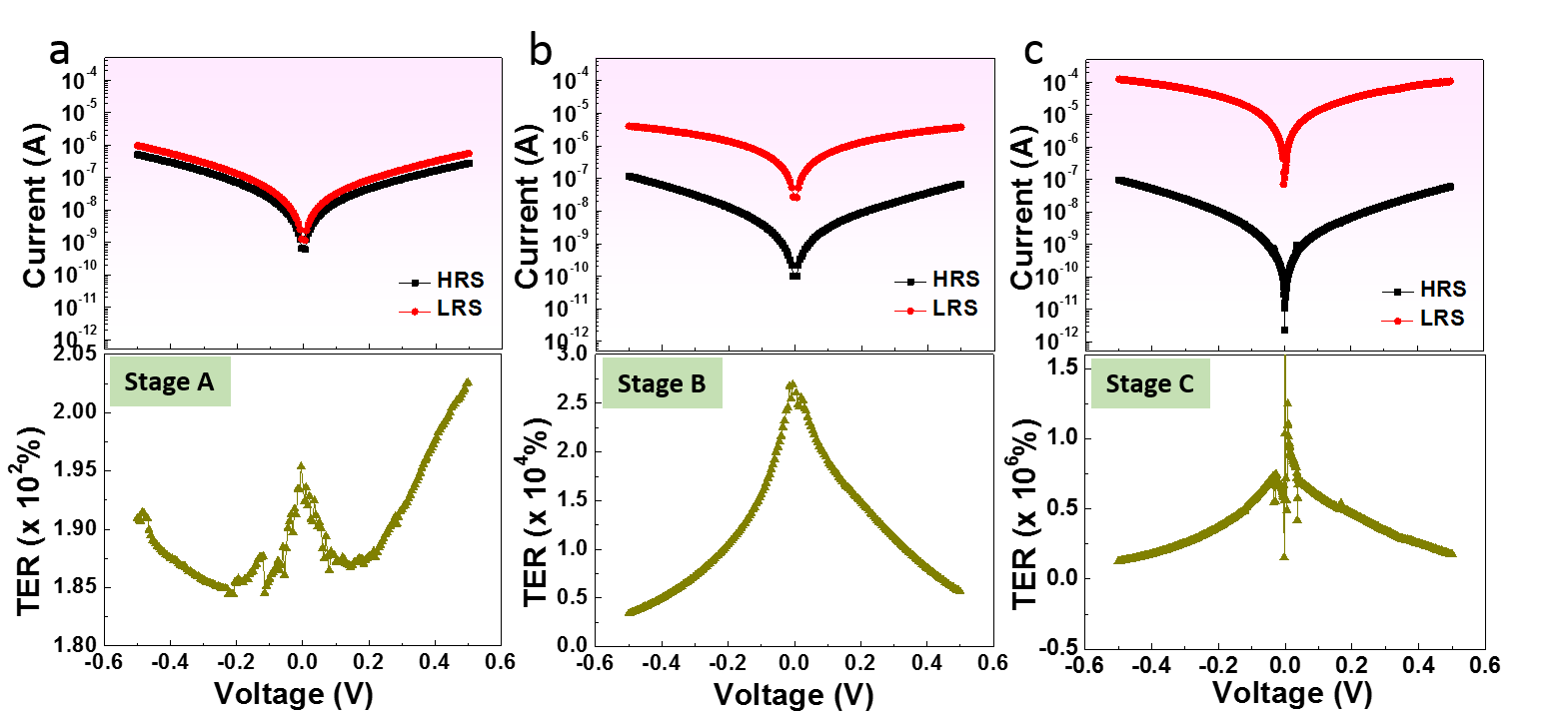
By the electrical pulse switching protocol shown in Fig.1b, the junction switches between the high resistance state, HRS (, after V+ pulse) and the low resistance state, LRS (, after V- pulse). A voltage pulse with amplitude as large as 6 V is used in order to obtain the maximum resistance contrast (TER 400) (see Fig.1c and ref.Wei et al. (2019)). In both HRS and LRS, TMR loops are obtained, as shown in Fig. 1d, leading to four resistance states (, , , , where the arrows signal the relative orientation of the electrodes magnetization). During the first few cycles, the TMR effect of the HRS () and LRS () are similar in magnitude (see Fig. 1d), indicating a negligible ME coupling, which differs from the strong coupling reported in perovskite tunnel barriers Garcia et al. (2010); Pantel et al. (2012); Yin et al. (2013). This stage, which we name stage A, is the one reported in ref.Wei et al. (2019). Interestingly, after a few tens of cycles, the behaviour changes substantially, reaching the stage B, as shown in Fig. 1e: the TMR sign is reversed from positive (HRS) to negative (LRS) indicating that the spin polarization is switched by the external electric field in a reversible manner, as shown in Fig. S1 (see also supplementary information). In addition, the coercive field of the harder ferromagnet (the Co layer) in the LRS (with negative TMR) increases by, approximately, a factor of two, compared to the switching fields of the HRS (with positive TMR). Moreover, the switching becomes sharper in the LRS. The increase of the coercive field and steep switching of the Co layer upon electrical cycling could originate in a modification of the HZO/Co interface.Bauer et al. (2015); Bauer, Emori, and Beach (2013). The number of cycles needed to reach the stage B has been found to differ depending on the junction under investigation.
With further electric cycling (stage C), the TMR signal becomes more noisy, as observed in Fig. 1f. The switching magnetic fields for the direct and reversed TMR become comparable but still higher than those of stage A (Fig. 1d). However, the magnitude of the TMR effect is not substantially altered. In the meantime, the two magnetic states are less well defined with less abrupt magnetic switching than the previous two stages, which could indicate an increasing number of defects introduced in the stack. For longer cycling time, with number of cycles depending on the junction, the TMR effect eventually disappears but the TER effect is still present.
The TMR sign has been reported to reverse by modification of the Co interface, either by adding an interface layerDe Teresa et al. (1999a); LeClair et al. (2001), or by the electric field-controlled hybridization at the interface (modified by the different ferroelectric polarization states)Pantel et al. (2012). These mechanisms affecting the Co/barrier interface are consistent with the changes, described above, of the magnetization switching of the Co layer upon electric cycling. However, since the reversed TMR is not observed in the A-stage (it only appears upon repeated electric cycling), the ferroelectric polarization switching can be discarded as the main contribution to the TMR sign reversal. Moreover, changes in the junctions by the introduction of oxygen vacancies (V) have also been reported to promote TMR sign reversalMarún et al. (2007). Given the possibility for positively charged V to migrate back and forth under the application of the electric field pulses with opposite polarities, we propose that ionic exchange is responsible for the observed changes of spin polarization, as well as the modification of the Co-HZO interface upon cycling.Bauer et al. (2015, 2012); Bauer, Emori, and Beach (2012).
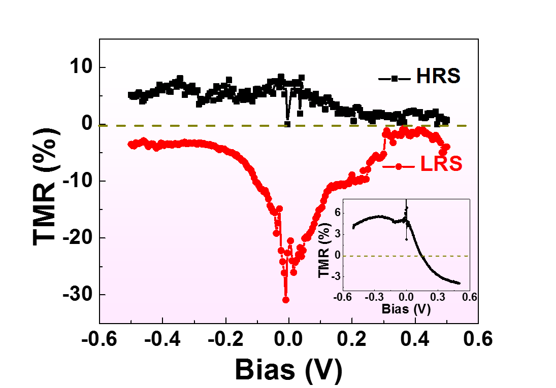
Focusing on stage C, from the I-V curves measured in parallel and anti-parallel magnetic states, we plot the bias dependence of the TMR for both HRS and LRS in Fig. 2. A striking feature is that in HRS state the TMR exhibits a very weak bias-dependence and is always positive; while in the LRS, the TMR is always negative with a rapid drop of TMR with increasing bias (absolute value), characteristic of thin-film MTJs and attributed to spin-flip scatteringMoodera, Nassar, and Mathon (1999). The electric field switching of spin polarization is, thus, evidenced over the whole investigated voltage range. Tuning of the read voltage allows to select the magnitude of the TMR change (e.g. Fig. 1f for -0.2 V read voltage). Looking at the bias-dependence of the TMR in the as-grown state for the same device (Fig. 2, inset), and noting that similar curves are obtained in both HRS and LRS at stage A for different junctions Wei et al. (2019), it is clear that electric field cycling completely changes the control of the spin polarization of the tunneling electrons. While the initial stage A shows a read voltage-controlled TMR sign change, already reported for Co-based junctionsDe Teresa et al. (1999b); Tsymbal et al. (2003); Wei et al. (2019), in stage C the TMR sign is wholly determined by the switchable resistance state of the device.
Concomitantly, the resistance ratio between the HRS and LRS (TER) also changes substantially during electric field cycling. By measuring the current-voltage (I-V) curves after positive and negative electric pulses, we can extract the TER at different bias by measuring the current ratio of HRS and LRS (). TER rises from to (stage A to C) with a large number of intermediate states, as shown in Figs. 3a-c, corresponding to Figs. 1d-f, respectively.
Thus, it is shown that the junctions are strongly affected by the very large electric fields applied across the ultrathin HZO barrier, which induce stage B and C with highly enhanced magnetoelectric coupling and very large TER, of great interest for devices. The driving voltages required to achieve these stages are close to the junction breakdown field. Therefore, the ability to keep cycling the device with such a large stimulus could be due to a voltage drop somewhere in the device, such as at the Co-HZO interface. Understanding the mechanisms leading to this evolution would crucially help finding the optimal conditions required for applications (typically 104-105 cycles Bez et al. (2003) for flash memory, and much higher endurance in other non-volatile memories, such as ferroelectric memory, magnetoresistive memory, resistive memory, etc.Boukhobza and Olivier (2017)).
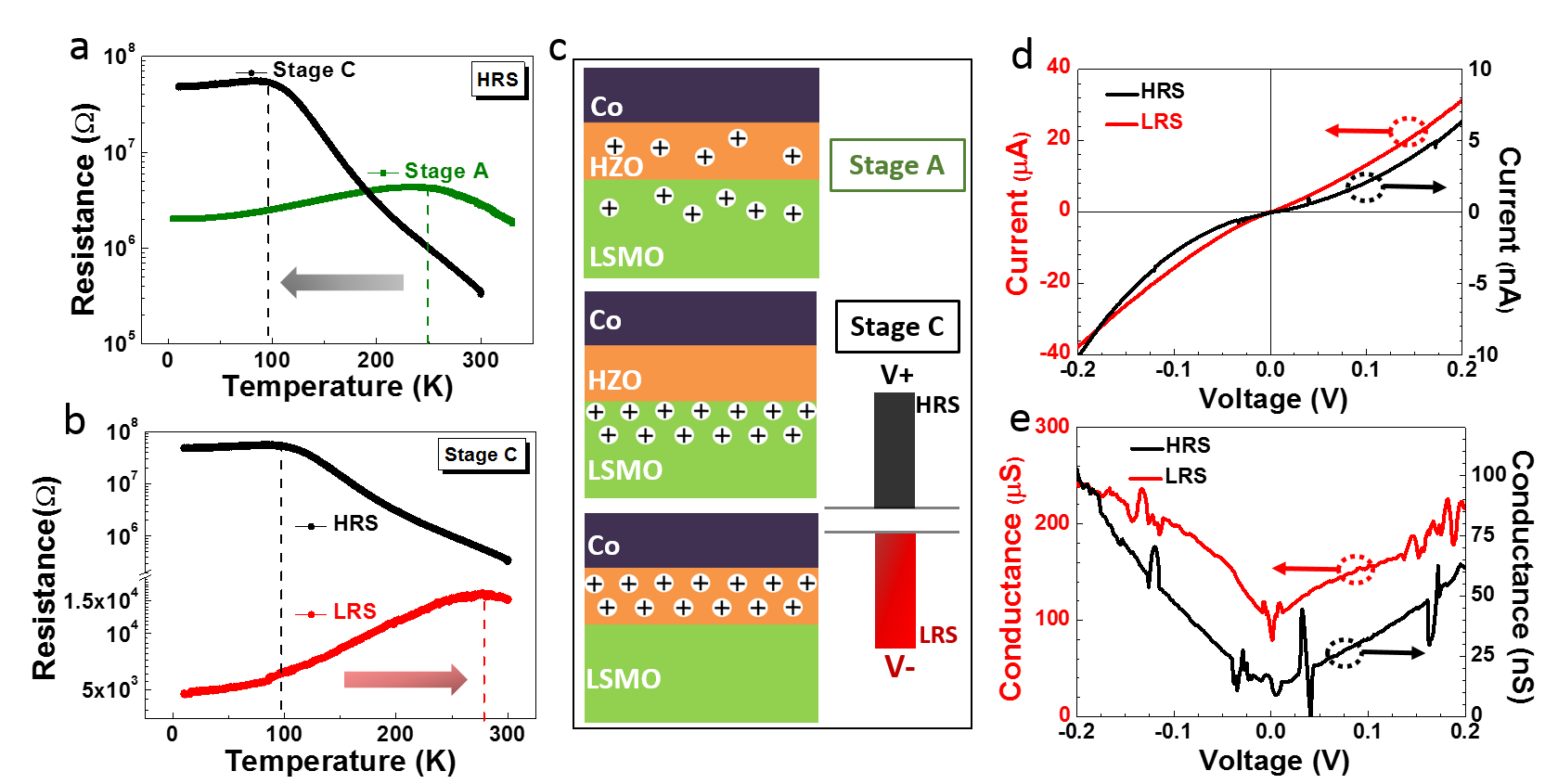
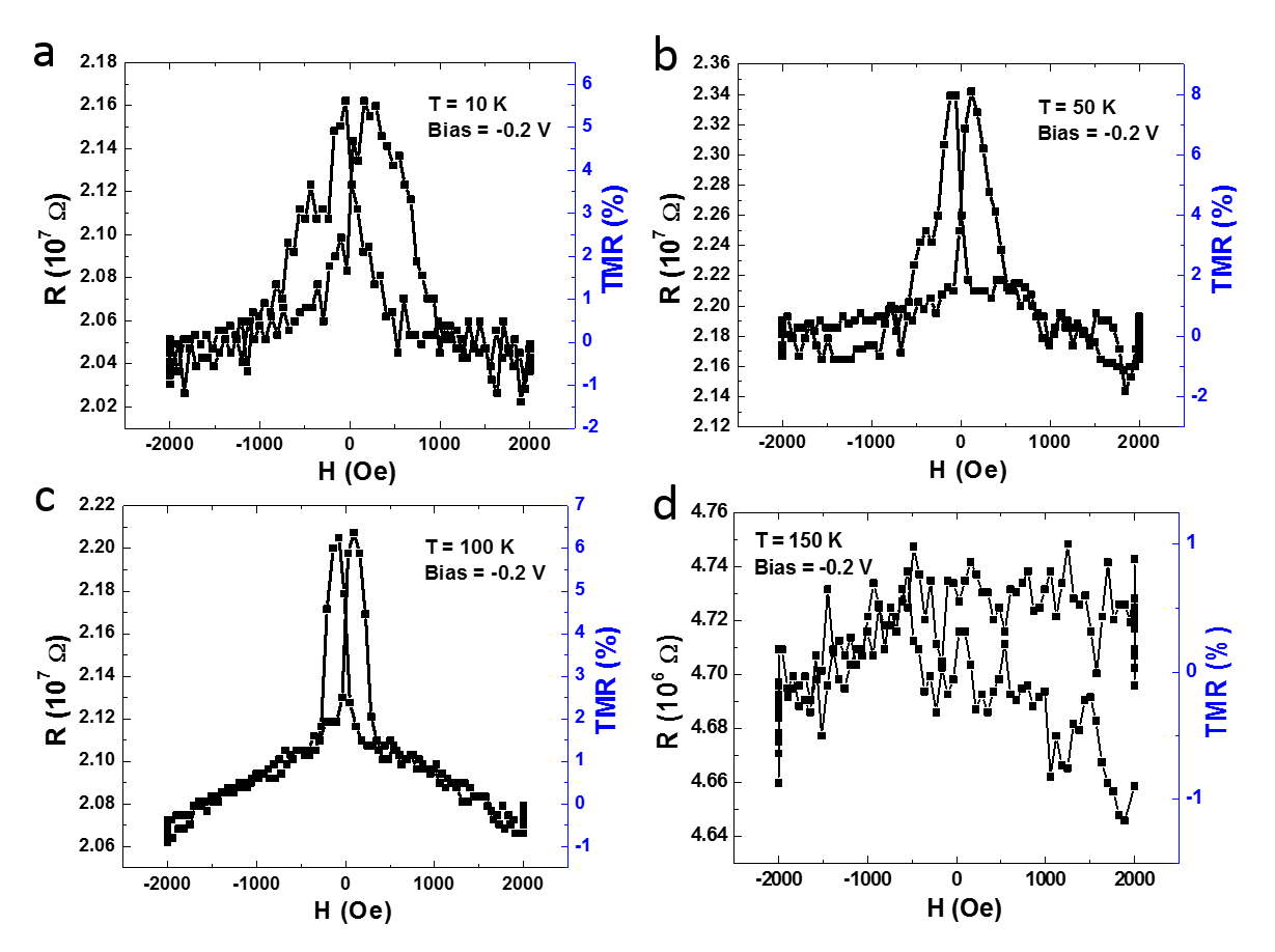
To shed light into the factors affecting the evolution from stage A to C by electric cycling, transport measurements of resistance versus temperature (R-T) are shown in Fig. 4a. The same junction is measured in the HRS in stage A (green) and stage C (black). In stage A, a metal-insulator transition happens at around 250 K. This is the temperature at which the ferromagnetic/metal-to-paramagnetic/insulator transition of LSMO at the interface with HZO takes place and, thus, where the TMR disappears.Wei et al. (2019) Upon electric field cycling, the transition temperature decreases. In Fig. 4a, the resistance of stage C (black) is shown to display the transition at around 100 K, which again coincides with the temperature at which TMR disappears (see Supplementary Fig. S2). The decrease of transition temperature from stage A to C is consistent with an oxygen deficiency at the LSMO interfaceCauro et al. (2001); Ge et al. (2015); Marún et al. (2007) that increases with repeated electric field cycling. In addition, the junction increases from stage A to C (see Fig. 1 and 3), which also agrees with an increasing content of oxygen vacancies in the LSMO layer at the HRS upon cycling, since oxygen vacancies are well known to reduce the carrier (hole) concentration in LSMO.Ge et al. (2015); Schlueter et al. (2012); Yao, Inkinen, and Van Dijken (2017); Cauro et al. (2001)
Furthermore, the R-T measurements at stage C (with large TER and strong ME coupling) in the HRS and LRS are shown in Fig. 4b. The transition temperature at the HRS (black), which had been lowered by the action of electric cycling to 100 K, increases up to 275 K, after the junction is brought to the LRS (red), which is higher than the transition temperature of the stage A ( 250 K, see Fig. 4a). This indicates that by applying a large negative pulse to the junction, the LSMO layer can reach an oxygen content larger than that of the initial stage. This is consistent with ionic exchange of oxygen vacancies in between the LSMO electrode and the HZO barrier during cycling, as represented in Fig. 4c. Giant resistive switching by oxygen vacancies migration has also been observed in different ferroelectric oxides tunnel barriersQin et al. (2016).
In Fig. 4c, we illustrate this possible scenario: in the as-grown state, both the LSMO and the HZO layers contain V (top panel). Upon electric field cycling, V are driven back and forth across the barrier. The evolution of the TER from % to % could be explained by the accumulation of the oxygen vacancies at the vicinity of the HZO/LSMO interface, thus increasing the V concentration that participates in the ionic exchange process. In this picture, the HRS is due to the oxygen vacancies being pushed into the LSMO electrode, resulting in a very resistive HZO/La0.7Sr0.3MnO3-δ contact. The LRS is obtained with the oxygen vacancies drifting back into the HZO barrier upon negative voltage pulse application, greatly reducing the resistivity of the junctionWaser et al. (2009). This gives rise to highly different current levels between HRS and LRS (large TER) as shown in Fig. 3c and Fig. 4d. Still, for both states, the non-linear I-V curves are similar (Fig. 4d) and the shape of the differential conductance curves (Fig. 4e) is compatible with tunneling conductionO’donnell et al. (2000), ruling out a drastic change of the conduction mechanism as probed by the investigated range of applied voltage.
An open question is the role of the ferroelectric polarization switching in these devices. Resistive switching by electric field has been reported in a wide variety of oxidesSawa (2008); Waser and Aono (2010); Waser et al. (2009), including binary oxides.Seo et al. (2004); Simmons and Verderber (1967); Choi et al. (2005) In the case of ferroelectric tunnel barriers, the profile of the electronic barrier can be modified by polarization reversal, thus causing strong TER effect. Rodrıguez Contreras et al. (2003); Gruverman et al. (2009) However, in our case, polarization switching is not the main contribution to the large TER, since it increases upon cycling from stage A to C, as shown in Fig. 3. It is interesting to notice that LSMO/HZO/Pt junctions, fabricated by I. Fina et al. Sulzbach et al. with the same material as tunnel barrier but with a double barrier thickness, also show TER values of around 400. This TER is reproducible with cycling under relatively smaller driving voltages (4 V), suggesting that this could be the contribution of the ferroelectric polarization. With higher driving voltage, larger TER similar to those reported here, are observed.Sulzbach et al.
In conclusion, TER values of up to coexisting with large ME coupling, by which the sign of the TMR effect is reversed with the electric field switching, have been achieved after cycling of Co/HZO/LSMO tunnel junctions with large enough electric fields. The temperature dependence of the transport behaviour is consistent with the exchange of oxygen vacancies at the LSMO/HZO interface, together with modifications of the HZO/Co interface. Next, an electrical protocol needs to be designed in order to increase the endurance of this state.
Methods
Thin films of Hf0.5Zr0.5O2 (HZO) barrier with thickness of 2 nm were grown by pulsed laser deposition (PLD) on FM La0.7Sr0.3MnO3(LSMO)-buffered (001)-SrTiO3 substrates. The thickness of LSMO film is around 30 nm. Details of the growth conditions can be found in ref.Wei et al. (2018). 50 nm FM Cobalt with a protective layer of Au (50nm), to preserve Co from oxidation, were deposited by sputtering on top of the HZO layer, to form the LSMO (FM) / HZO (FE)/ Co (FM) stacks. Junctions with different sizes, ranging from to , are fabricated (see details in ref.Wei et al. (2019)). The electrical measurements are performed using a Keithley 237 source measurement unit and a Keithley 4200A-SCS parameter analyzer, and the temperature environment and magnetic field are supplied by a Physical Properties Measurement System (PPMS) by Quantum Design. As shown in the schematic drawing in Fig. 1a, the voltage source is applied on the LSMO/HZO/Co stack with bottom electrode grounded (for a positive bias, the electrons are tunneling from LSMO to Co). The magnetic field is swept along the easy magnetization axis of LSMO in the [110] direction.
Acknowledgements
The authors are grateful to Tamalika Banerjee and Manuel Bibes for useful discussions. YW and BN acknowledge a China Scholarship Council grant and a Van Gogh travel grant.
References
- Gajek et al. (2007) M. Gajek, M. Bibes, S. Fusil, K. Bouzehouane, J. Fontcuberta, A. Barthelemy, and A. Fert, Nature Materials 6, 296 (2007).
- Rodrıguez Contreras et al. (2003) J. Rodrıguez Contreras, H. Kohlstedt, U. Poppe, R. Waser, C. Buchal, and N. Pertsev, Applied Physics Letters 83, 4595 (2003).
- Tsymbal et al. (2012) E. Y. Tsymbal, A. Gruverman, V. Garcia, M. Bibes, and A. Barthélémy, MRS bulletin 37, 138 (2012).
- Scott (2007) J. Scott, Nature Materials 6, 256 (2007).
- Hur et al. (2004) N. Hur, S. Park, P. Sharma, J. Ahn, S. Guha, and S. Cheong, Nature 429, 392 (2004).
- Bibes and Barthélémy (2008) M. Bibes and A. Barthélémy, Nature Materials 7, 425 (2008).
- Ortega et al. (2015) N. Ortega, A. Kumar, J. Scott, and R. S. Katiyar, Journal of Physics: Condensed Matter 27, 504002 (2015).
- Webster (2002) J. Webster, Biomedical Instrumentation & Technology 36 (2002).
- Eerenstein, Mathur, and Scott (2006) W. Eerenstein, N. Mathur, and J. F. Scott, Nature 442, 759 (2006).
- Ramesh and Spaldin (2007) R. Ramesh and N. A. Spaldin, Nature Materials 6, 21 (2007).
- Fiebig (2005) M. Fiebig, Journal of Physics D: Applied Physics 38, R123 (2005).
- Garcia et al. (2010) V. Garcia, M. Bibes, L. Bocher, S. Valencia, F. Kronast, A. Crassous, X. Moya, S. Enouz-Vedrenne, A. Gloter, D. Imhoff, et al., Science 327, 1106 (2010).
- Yin and Li (2017) Y. Yin and Q. Li, Journal of Materiomics 3, 245 (2017).
- Dong, Xiang, and Dagotto (2019) S. Dong, H. Xiang, and E. Dagotto, National Science Review 6, 1 (2019).
- Dong et al. (2015) S. Dong, J.-M. Liu, S.-W. Cheong, and Z. Ren, Advances in Physics 64, 519 (2015).
- Bauer et al. (2015) U. Bauer, L. Yao, A. J. Tan, P. Agrawal, S. Emori, H. L. Tuller, S. Van Dijken, and G. S. Beach, Nature Materials 14, 174 (2015).
- Lee et al. (2010) J. H. Lee, L. Fang, E. Vlahos, X. Ke, Y. W. Jung, L. F. Kourkoutis, J.-W. Kim, P. J. Ryan, T. Heeg, M. Roeckerath, et al., Nature 466, 954 (2010).
- Fabrèges et al. (2009) X. Fabrèges, S. Petit, I. Mirebeau, S. Pailhès, L. Pinsard, A. Forget, M. Fernandez-Diaz, and F. Porcher, Physical Review Letters 103, 067204 (2009).
- Tsymbal and Kohlstedt (2006) E. Y. Tsymbal and H. Kohlstedt, Science 313, 181 (2006).
- Rondinelli, Stengel, and Spaldin (2008) J. M. Rondinelli, M. Stengel, and N. A. Spaldin, Nature Nanotechnology 3, 46 (2008).
- Böscke et al. (2011) T. Böscke, J. Müller, D. Bräuhaus, U. Schröder, and U. Böttger, Applied Physics Letters 99, 102903 (2011).
- Park et al. (2015) M. H. Park, Y. H. Lee, H. J. Kim, Y. J. Kim, T. Moon, K. D. Kim, J. Mueller, A. Kersch, U. Schroeder, T. Mikolajick, et al., Advanced Materials 27, 1811 (2015).
- Shimizu et al. (2016) T. Shimizu, K. Katayama, T. Kiguchi, A. Akama, T. J. Konno, O. Sakata, and H. Funakubo, Scientific Reports 6, 32931 (2016).
- Wei et al. (2018) Y. Wei, P. Nukala, M. Salverda, S. Matzen, H. J. Zhao, J. Momand, A. S. Everhardt, G. Agnus, G. R. Blake, P. Lecoeur, et al., Nature Materials 17, 1095 (2018).
- Lyu et al. (2018) J. Lyu, I. Fina, R. Solanas, J. Fontcuberta, and F. Sánchez, Applied Physics Letters 113, 082902 (2018).
- Lyu et al. (2019) J. Lyu, I. Fina, R. Solanas, J. Fontcuberta, and F. Sánchez, ACS Applied Electronic Materials 1, 220 (2019).
- Wei et al. (2019) Y. Wei, S. Matzen, G. Agnus, M. Salverda, P. Nukala, T. Maroutian, Q. Chen, J. Ye, P. Lecoeur, and B. Noheda, arXiv preprint arXiv:1902.08021 (2019).
- Pantel et al. (2012) D. Pantel, S. Goetze, D. Hesse, and M. Alexe, Nature Materials 11, 289 (2012).
- Yin et al. (2013) Y. Yin, J. Burton, Y. M. Kim, A. Y. Borisevich, S. J. Pennycook, S. M. Yang, T. Noh, A. Gruverman, X. Li, E. Tsymbal, et al., Nature Materials 12, 397 (2013).
- Bauer, Emori, and Beach (2013) U. Bauer, S. Emori, and G. S. Beach, Nature Nanotechnology 8, 411 (2013).
- De Teresa et al. (1999a) J. M. De Teresa, A. Barthelemy, A. Fert, J. P. Contour, F. Montaigne, and P. Seneor, Science 286, 507 (1999a).
- LeClair et al. (2001) P. LeClair, B. Hoex, H. Wieldraaijer, J. Kohlhepp, H. Swagten, and W. De Jonge, Physical Review B 64, 100406 (2001).
- Marún et al. (2007) I. V. Marún, F. Postma, J. Lodder, and R. Jansen, Physical Review B 76, 064426 (2007).
- Bauer et al. (2012) U. Bauer, M. Przybylski, J. Kirschner, and G. S. Beach, Nano Letters 12, 1437 (2012).
- Bauer, Emori, and Beach (2012) U. Bauer, S. Emori, and G. S. Beach, Applied Physics Letters 100, 192408 (2012).
- Moodera, Nassar, and Mathon (1999) J. S. Moodera, J. Nassar, and G. Mathon, Annual Review of Materials Science 29, 381 (1999).
- De Teresa et al. (1999b) J. De Teresa, A. Barthélémy, A. Fert, J. Contour, R. Lyonnet, F. Montaigne, P. Seneor, and A. Vaures, Physical Review Letters 82, 4288 (1999b).
- Tsymbal et al. (2003) E. Y. Tsymbal, A. Sokolov, I. Sabirianov, and B. Doudin, Physical Review Letters 90, 186602 (2003).
- Bez et al. (2003) R. Bez, E. Camerlenghi, A. Modelli, and A. Visconti, Proceedings of the IEEE 91, 489 (2003).
- Boukhobza and Olivier (2017) J. Boukhobza and P. Olivier, Flash Memory Integration: Performance and Energy Issues (Elsevier, 2017).
- Cauro et al. (2001) R. Cauro, A. Gilabert, J. Contour, R. Lyonnet, M.-G. Medici, J.-C. Grenet, C. Leighton, and I. K. Schuller, Physical Review B 63, 174423 (2001).
- Ge et al. (2015) C. Ge, K.-J. Jin, L. Gu, L.-C. Peng, Y.-S. Hu, H.-Z. Guo, H.-F. Shi, J.-K. Li, J.-O. Wang, X.-X. Guo, et al., Advanced Materials Interfaces 2, 1500407 (2015).
- Schlueter et al. (2012) C. Schlueter, P. Orgiani, T.-L. Lee, A. Y. Petrov, A. Galdi, B. Davidson, J. Zegenhagen, and C. Aruta, Physical Review B 86, 155102 (2012).
- Yao, Inkinen, and Van Dijken (2017) L. Yao, S. Inkinen, and S. Van Dijken, Nature Communications 8, 14544 (2017).
- Qin et al. (2016) Q. H. Qin, L. Äkäslompolo, N. Tuomisto, L. Yao, S. Majumdar, J. Vijayakumar, A. Casiraghi, S. Inkinen, B. Chen, A. Zugarramurdi, et al., Advanced Materials 28, 6852 (2016).
- Waser et al. (2009) R. Waser, R. Dittmann, G. Staikov, and K. Szot, Advanced Materials 21, 2632 (2009).
- O’donnell et al. (2000) J. O’donnell, A. Andrus, S. Oh, E. Colla, and J. Eckstein, Applied Physics Letters 76, 1914 (2000).
- Sawa (2008) A. Sawa, Materials Today 11, 28 (2008).
- Waser and Aono (2010) R. Waser and M. Aono, in Nanoscience And Technology: A Collection of Reviews from Nature Journals (World Scientific, 2010) pp. 158–165.
- Seo et al. (2004) S. Seo, M. Lee, D. Seo, E. Jeoung, D.-S. Suh, Y. Joung, I. Yoo, I. Hwang, S. Kim, I. Byun, et al., Applied Physics Letters 85, 5655 (2004).
- Simmons and Verderber (1967) J. Simmons and R. Verderber, Proceedings of the Royal Society of London. Series A. Mathematical and Physical Sciences 301, 77 (1967).
- Choi et al. (2005) B. Choi, D. S. Jeong, S. Kim, C. Rohde, S. Choi, J. Oh, H. Kim, C. Hwang, K. Szot, R. Waser, et al., Journal of Applied Physics 98, 033715 (2005).
- Gruverman et al. (2009) A. Gruverman, D. Wu, H. Lu, Y. Wang, H. Jang, C. Folkman, M. Y. Zhuravlev, D. Felker, M. Rzchowski, C.-B. Eom, et al., Nano Letters 9, 3539 (2009).
- (54) M. C. Sulzbach, J. Lyu, X. Long, F. Sánchez, I. Fina, and J. Fontcuberta, Talk in EMRS Spring meeting 2019, Nice .