Disorder effects in InAs/GaSb topological insulator candidates
Abstract
We report the theoretical investigation of the disorder effects on the bulk states of inverted InAs/GaSb quantum wells. As disorder sources we consider the interface roughness and donors/acceptors supplied by intentional doping. We use a approach combined with a numerical diagonalization of the disordered Hamiltonian to get a full insight of the disordered eigenenergies and eigenfunctions of the electronic system. While interface roughness slightly pertubs the carrier motion, we show that dopants strongly bind and localize the bulk states of the structure. Moreover, both types of scatterers strengthen the intrinsic hybridization between holes and electrons in the structure.
pacs:
73.21.Ac,78.67.PtI Introduction
Topological insulators are phases of matter characterized by an insulating gap and protected conducting surface (or edge) states Hasan and Kane (2010). In two-dimensional (2D) structures, these phases manifest themselves by the formation of helical channels at the edges of an insulating 2D electronic system, giving rise to the so-called Quantum Spin Hall Effect (QSHE). After its theoretical prediction Bernevig and Zhang (2006); Bernevig et al. (2006) and its first experimental demonstration in HgTe quantum wells (QWs) König et al. (2007), it has been predicted that InAs/GaSb QWs should also be promising 2D topological insulator candidates Liu et al. (2008). Similarly to HgTe QWs, InAs/GaSb QWs have unique band alignments that display a subband inversion transition as a function of the layer thickness. Moreover, due to their type II alignment (where the confinement of holes and electrons occurs in two different layers), InAs/GaSb QWs have the additional advantage of being electrically tunable through the phase transition Yang et al. (1997); Cooper et al. (1998).
A non-local transport through edge states has been already reported in inverted InAs/GaSb (QWs) Knez et al. (2011); Nichele et al. (2014); Mueller et al. (2015). However, a substantial bulk conductivity still degrades the visibility of the dissipationless edge channels indicating that the bulk is rather a metallic system. A few solutions have so far been proposed such as the intentional addition of disorder in the sample to lower the bulk mobility and suppress the parasitic channels Suzuki et al. (2013); Charpentier et al. (2013); Du et al. (2015). In contrast to experimental studies, there has been little theoretical work done on disordered inverted InAs/GaSb QWs. A theoretical study of QSH states in doped InAs/GaSb QWs has been reported by Xu et al. Xu et al. (2014), showing that an intentional Si-doping leads to the opening of a mobility gap. In this work, the dopants were considered as delta-like scatterers within the tight-binding approach, not accounting for the actual long-range of the Coulomb interactions. This approach is sufficient to predict the existence of in-gap localized states but is not adequate to get a quantitative description of the disordered bulk states in these complex structures.
In this paper, we present a theoretical analysis of the disorder effects on the bulk states in inverted InAs/GaSb QWs based on realistic disorder modellings. We combine an eight-band model and a numerical diagonalization of the disordered Hamiltonian within the envelope function formalism. This approach is more appropriate for the description of slowly varying potentials like Coulomb potentials and allows an accurate determination of the band dispersion of the non-disordered structure as well as a full treatment of the carrier-disorder interactions.
Our paper is organized as follows. In Sec. II, we first present our model of disorder where we concentrate on two types of static scatterers: the interface roughness and the donors/acceptors supplied by intentional doping. Then, in Sec. III we describe our theoretical approach based on the model for the computation of the unperturbed states of a AlAs/InAs/GaSb/AlAs heterostructure and the numerical diagonalization of the disordered Hamiltonian expanded in this unperturbed basis. Finally, in Secs. IV and V, we report the different disorder effects such as the binding effects and the spatial localization of the states as well as the disorder-induced hybridization between valence and conduction carriers.
II Model of disorder
The interface roughness results from the interdiffusion of the layers during the growth process. Therefore it is an unavoidable source of scattering in heterostructures. In the envelope function formalism, the interface defects can be modeled by randomly distributed Gaussian protusions either from the InAs layer in the GaSb one (attractive defects) or vice versa (repulsive defects) Ndebeka-Bandou et al. (2012). Using this model and considering a single interface located at ( defines the growth axis), we write the disorder potential as:
| (1) |
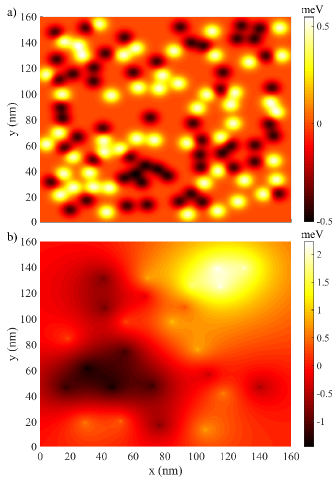
where () for repulsive (attractive) defects and with the Heaviside function. The roughness height is set to two monolayers. The in-plane coordinates are random and locate the protusion on the surface of the sample. The in-plane extension of the defects and the band offset discontinuity are set to nm and 150 meV respectively while the number of defects is fixed by the fractional coverage of the surface . In our model, the numbers of attractive and repulsive defects are equal. Figure 1a shows the potential energy created by a random distribution of interface defects in a AlAs/InAs/GaSb/AlAs quantum well.
Due to their ability to bind and localize states Ndebeka-Bandou et al. (2013a), dopants are also known to be a relevant source of scattering in heterostructures. We consider the doping configuration that has been experimentally realized by Du et al. Du et al. (2015) where one monolayer of Si atoms of concentration cm-2 is grown at the InAs/GaSb interface. Since Si atoms behave as donors in InAs and as acceptors in GaSb Shen et al. (1993), the densities of donors and acceptors are both equal to in our model. Like interface defects, the dopants are randomly distributed in the layer plane located at the InAs/GaSb interface. Accounting for screening effects by the mobile carriers, the disorder potential is described by a Yukawa-like potential with Debye screening length Ndebeka-Bandou et al. (2016):
| (2) |
where , is the elementary charge, and are the dielectric constants of the vacuum and the material respectively. The prefactor equals () for acceptors (donors). Figure 1b shows the potential energy created by a random distribution of coulombic donors and acceptors in the same structure as in Fig. 1a.
III model and numerical diagonalization
As previously, we consider a 15 nm/8 nm InAs/GaSb QW embedded in two wide gap AlSb barriers of thickness 50 nm. In the presence of disorder, the one-particle envelope Hamiltonian is
| (3) |
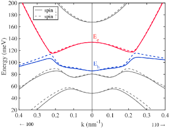
where is the Hamiltonian in absence of disorder and is the disorder potential either equal to or . We compute the eigenstates of , i.e. the subband dispersion and the spinor wavefunctions , for all directions by using the eight-band model developped in Ref. Zakharova et al., 2001. labels the different subbands and is the in-plane momentum. The direction (001) coincides with the growth axis and the material parameters are taken from Ref. Halvorsen et al., 2000.
Figure 2 shows the calculated subband dispersion of the InAs/GaSb QW along the (100) and (110) directions for the two spin orientations. As expected from the layer ratio, the structure exhibits a band-inversion characterized by multiple anti-crossings at finite values, along with the opening of a hybridization gap between the conduction subband and the valence one . Moreover, due to the asymmetry of the confining potential, the spin degeneracy is lifted at finite . This results in a significant dependence of the dispersion upon the spin orientation de Andrada e Silva et al. (1997). The spin-up dispersion has a gap of about 6 meV while the spin-down dispersion is nearly gapless (an energy gap of less than 1 meV is extracted from the data). Since such a small gap is not wide enough to prevent parasitic scatterings between the conduction and valence bulk states, this local closing of the energy gap can be readily identified as the main cause of the metallic behaviour of the structure observed experimentally.
In the following, we consider the case where the Fermi level lays inside the hybridization gap. Thus, for the numerical diagonalization of , we restrict our consideration to the two subbands of interest: and (see Fig. 2). Since is spin-independent, the results obtained for a given spin orientation are qualitatively similar to those obtained for the opposite spin orientation, the difference between the two configurations mainly resides in the size of the energy gap.
The calculation of the eigenstates of (3) is performed by a numerical diagonalization of in the two-subband basis of periodic plane waves (Born-von Karman boundary conditions) on a nm2 finite sample Ndebeka-Bandou et al. (2012). The wavefunctions of the basis states are
| (4) |
where . For a basis formed by periodic plane waves, the Hamiltonian is expressed as the following block matrix
| (5) |
The diagonal blocks in (5) contain the intra-subband coupling terms:
| (6) |
while the off-diagonal blocks contain the inter-subband coupling terms
| (7) |
In (6) and (7), the matrix elements of the disorder potential are calculated the same way as in Ref. Ndebeka-Bandou et al., 2014.
The disorder breaks the in-plane translational invariance, giving rise to a set of discrete energy levels for the energy spectrum. Consequently, the in-plane momentum is no longer a good quantum number and must be replaced by a discrete index , namely:
| (8) |
where the ’s are the eigenvalues of . Their corresponding eigenfunctions are then written as
| (9) |
where the coefficients are the coordinates of the eigenvectors of associated with the eigenvalue . This approach consists of a full treatment of the static disorder where the only assumption lies in the choice of the expression and the parameters of . Due to the randomness of the disorder potential, the diagonalization of is repeated for a large number of random realizations. The quantities that are showed in the following are the results of an averaging over a large set of random trials.
IV Binding and localization effects
As a first noticeable effect, the disorder reorganizes the energy spectrum of the system. Figure 3 displays the density of states (DOS) in three different configurations: without disorder, with interface roughness and with Si-dopants. The results for the spin-down and spin-up orientations are shown in Fig. 3a and 3b respectively. Both types of scatterers create states below (for conduction states due to attractive potentials) and above (for valence states due to repulsive potentials) the subband edges. The effect of interface roughness is quantitatively much smaller.
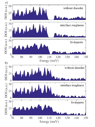
Extremely shallow bound states with typical binding energies of 0.3-0.5 meV below/above the subband edges are found whereas binding energies of dopants reach 2-3 meV and tend to close the energy gap. This very weak binding effect by the interface defects originates from the shorter-range and smaller-depth compared to the fluctuations of the Coulomb potential. Note also that in type II QWs, the carriers are mostly confined in each layer and therefore have a weak probability density at the interface Zakharova et al. (2001), where both interface defects and dopants are actually located. This reduces the potential strength of both scatterers Ndebeka-Bandou et al. (2013b). Similarly, bound states are also found for the spin-up orientation. However, a plot of the DOS cannot reveal their existence due to the quasi-absence of energy gap. In Fig. 3b one can still notice a broadening of the DOS arising from the lifting of degeneracy of the states by the dopants.
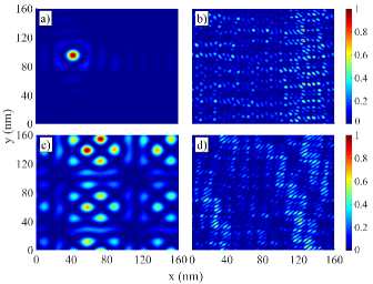
Another way to evidence bound states is to evaluate their spatial localization. Bound states emerge from multi-scattering events and have the particularity to be spatially localized in the layer plane due to the admixture of the carrier in-plane wavefunctions by the disorder Ndebeka-Bandou et al. (2013a). Fig. 4 displays the in-plane probability density of disordered states at various energies in the presence of dopants (upper panels) and interface defects (lower panels). In-gap states are strongly localized by the dopants, as shown in Fig. 4a, whereas continuum states remain extended (see Fig. 4b). As shown in Fig. 4c, the localization by interface roughness of shalow bound states is weak. The continuum states in both disorder configurations have a similar extension as shown in Figs. 4b and 4b.
One way to quantify this localization effect is to compute the in-plane localization length of the disordered states. The in-plane localization can be defined as
| (10) |
where is the in-plane part of the wavefunction obtained by integrating the modulus square of (9) over .
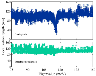
Figure 5 shows the localization length of the spin-up eigenstates. The spatial localization by the dopants is significantly more pronounced, especially close to the subband edges (around 116 meV, see also Fig. 1) where a mobility gap of about 4 meV opens. On the other hand, the localization by interface defects remains weak as expected from the in-plane probability density computed in Figs. 4c and 4d. Similar features are found for the spin-down states.
These results are consistent with the experimental observations Du et al. (2015) and the results found by Xu et al. with the tight-binding formalism and additionally provide a quantitative estimate of the binding energies and localization lengths. In particular, a localization of the continuum states by dopants is found to be about 25% compared to non-disordered extended states on a 160160 nm2 surface foo . An intentional doping certainly closes the energy gap and decreases the bulk conductivity by opening a mobility gap but also disturbs the remaining extended states.
V Disorder-induced hybridization
The in-plane localization result from the strong admixture of the states by the disorder. In absence of scatterer, each state is associated with a single plane wave of wavevector , but in disordered samples contains several contributions in its expansion (9). In the previous section, we have shown the consequence of this adxmiture on the in-plane carrier motion, but this mixing also translates into a strong admixture of the wavefunctions for the motion along the direction. To illustrate this effect, we define the normalized probability density of the eigenstates in each layer as:
| (11) |
where is the -part of the disordered wavefunctions obtained by integrating over the plane. Figure 6 displays the energy dependence of and for the spin-up orientation (similar results are obtained for the spin-down states, not shown here). One particularity of the type II alignment is that the confinement along the growth axis of the conduction and valence states does not occur in the same layer.
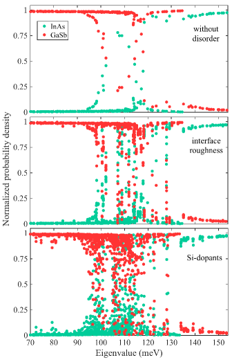
As shown in the upper panel of Fig. 6, without disorder and far from the subband edges (for energies meV and meV), the conduction carriers are confined in the InAs layer while the valence carriers are confined in the GaSb layer. Near the subband edges, or in other words in the inverted region ( meV meV), the confining layer varies from InAs to GaSb reflecting the band inversion and the hybridization of the valence and conduction states in this energy range. Values of lower than and close to 0.5 indicate a delocalization of strongly hybridized wavefunctions over the two layers. As shown in Fig. 6, the static disorder strengthens this intrinsic hybridization. The number of delocalized states increases and the hybridization region becomes wider. These features are again found to be weaker for interface roughness than for Si-dopants. Finally, it is important to remark that such delocalization effects along the growth axis are specific to inverted QWs. In non-inverted semiconductor QWs, where there is no electron-hole admixture, no disorder-induced hybridization is expected.
VI Conclusion
We have theoretically investigated the effects of the interface roughness and Si-dopants on the bulk states of an inverted InAs/GaSb QW. The combination of calculations and numerical diagonalizations enable to get a deep understanding and a full characterization of the disordered energy spectrum and eigenfunctions of the system. We found that an intentional doping leads to the opening of a mobility gap in the vicinity of the conduction and valence subband edges despite the closing of the energy gap due to the formation of in-gap bound states. This result is in agreement with the features found by the tight-binding approach and can be identified as being the origin of a decrease of the bulk conductance in actual samples. The interface roughness, for its part, generates a potential that is too weak to significantly localize the bulk states and only perturbs marginally their energy spectrum. On the other hand, both types of scatterer affect the remaining extended states and strengthen the intrinsic hybridization of electrons and holes.
Acknowledgements.
C-NB thanks Dr. K. Ohtani, Dr. A. Soluyanov and Pr. G. Bastard for fruitful and valuable discussions and gratefully acknowledges the support from the ERC under the project MUSiC.References
- Hasan and Kane (2010) M. Z. Hasan and C. L. Kane, Rev. Mod. Phys. 82, 3045 (2010).
- Bernevig and Zhang (2006) B. A. Bernevig and S.-C. Zhang, Phys. Rev. Lett. 96, 106802 (2006).
- Bernevig et al. (2006) B. A. Bernevig, T. L. Hughes, and S.-C. Zhang, Science 314, 1757 (2006).
- König et al. (2007) M. König, S. Wiedmann, C. Brüne, A. Roth, H. Buhmann, L. W. Molenkamp, X.-L. Qi, and S.-C. Zhang, Science 318, 766 (2007).
- Liu et al. (2008) C. Liu, T. L. Hughes, X.-L. Qi, K. Wang, and S.-C. Zhang, Phys. Rev. Lett. 100, 236601 (2008).
- Yang et al. (1997) M. J. Yang, C. H. Yang, B. R. Bennett, and B. V. Shanabrook, Phys. Rev. Lett. 78, 4613 (1997).
- Cooper et al. (1998) L. J. Cooper, N. K. Patel, V. Drouot, E. H. Linfield, D. A. Ritchie, and M. Pepper, Phys. Rev. B 57, 11915 (1998).
- Knez et al. (2011) I. Knez, R.-R. Du, and G. Sullivan, Phys. Rev. Lett. 107, 136603 (2011).
- Nichele et al. (2014) F. Nichele, A. N. Pal, P. Pietsch, T. Ihn, K. Ensslin, C. Charpentier, and W. Wegscheider, Phys. Rev. Lett. 112, 036802 (2014).
- Mueller et al. (2015) S. Mueller, A. N. Pal, M. Karalic, T. Tschirky, C. Charpentier, W. Wegscheider, K. Ensslin, and T. Ihn, Phys. Rev. B 92, 081303 (2015).
- Suzuki et al. (2013) K. Suzuki, Y. Harada, K. Onomitsu, and K. Muraki, Phys. Rev. B 87, 235311 (2013).
- Charpentier et al. (2013) C. Charpentier, S. Fält, C. Reichl, F. Nichele, A. Nath Pal, P. Pietsch, T. Ihn, K. Ensslin, and W. Wegscheider, Applied Physics Letters 103, 112102 (2013), 10.1063/1.4821037.
- Du et al. (2015) L. Du, I. Knez, G. Sullivan, and R.-R. Du, Phys. Rev. Lett. 114, 096802 (2015).
- Xu et al. (2014) D.-H. Xu, J.-H. Gao, C.-X. Liu, J.-H. Sun, F.-C. Zhang, and Y. Zhou, Phys. Rev. B 89, 195104 (2014).
- Ndebeka-Bandou et al. (2012) C. Ndebeka-Bandou, F. Carosella, R. Ferreira, A. Wacker, and G. Bastard, Applied Physics Letters 101, 191104 (2012).
- Ndebeka-Bandou et al. (2013a) C. Ndebeka-Bandou, F. Carosella, R. Ferreira, and G. Bastard, Applied Physics Letters 102, 191105 (2013a), 10.1063/1.4804551.
- Shen et al. (1993) J. Shen, J. D. Dow, S. Y. Ren, S. Tehrani, and H. Goronkin, Journal of Applied Physics 73, 8313 (1993).
- Ndebeka-Bandou et al. (2016) C. Ndebeka-Bandou, F. Carosella, and G. Bastard, Journal of Applied Physics 119, 095703 (2016), 10.1063/1.4942848.
- Zakharova et al. (2001) A. Zakharova, S. T. Yen, and K. A. Chao, Phys. Rev. B 64, 235332 (2001).
- Halvorsen et al. (2000) E. Halvorsen, Y. Galperin, and K. A. Chao, Phys. Rev. B 61, 16743 (2000).
- de Andrada e Silva et al. (1997) E. A. de Andrada e Silva, G. C. La Rocca, and F. Bassani, Phys. Rev. B 55, 16293 (1997).
- Ndebeka-Bandou et al. (2014) C. Ndebeka-Bandou, F. Carosella, R. Ferreira, A. Wacker, and G. Bastard, Semiconductor Science and Technology 29, 023001 (2014).
- Ndebeka-Bandou et al. (2013b) C. Ndebeka-Bandou, A. Wacker, F. Carosella, R. Ferreira, and G. Bastard, Applied Physics Express 6, 094101 (2013b).
- (24) An unperturbed state would be perfectly extended in the layer plane and would have a localization length equal to the sample size, in the present case 160 nm .