Electronic Stripes and Transport Properties in Borophene Heterostructures
Abstract
We performed a theoretical investigation of the structural and electronic properties of (i) pristine, and (ii) superlattice structures of borophene. In (i), by combining first-principles calculations, based on the density functional theory (DFT), and simulations of the X-ray Absorption Near-Edge Structure (XANES) we present a comprehensive picture connecting the atomic arrangement of borophene and the X-ray absorption spectra. Once we have characterized the electronic properties of the pristine systems, we next examined the electronic confinement effects in 2D borophene superlattices (BSLs) [(ii)]. Here, the BSL structures were made by attaching laterally two different structural phases of borophene. The energetic stability, and the electronic properties of those BSLs were examined based on total energy DFT calculations. We find a highly anisotropic electronic structure, characterized by the electronic confinement effects, giving rise to “electronic stripes”, and metallic channels ruled by the superlattices. Combining DFT and the Landauer-Büttiker formalism, we investigate the electronic transport properties in BSLs. Our results of the transmission probability reveal that the electronic transport is ruled by or a combination of and transmission channels, depending on the atomic arrangement and periodicity of the superlattices. Finally, we show that there is huge magnification on the directional dependence of the electronic transport properties in BSLs, in comparison with the pristine borophene phase. Those findings indicate that BSLs are quite interesting systems in order to design conductive nanoribbons in a 2D platform.
I Introduction
Since the breakthrough of graphene in 2004,Novoselov et al. (2004) the synthesis of two dimensional (2D) materials reached the state of the art. The formation of the honeycomb lattice in graphene is dictated by the C- hybridization of the carbon atoms, favoring the formation of two dimensional systems. Such an electronic/orbital “ingredient” is also present in boron atoms (B-), and thus pointing out the possibility of synthesis of 2D boron systems.
Indeed, there are several theoretical studies, based on first-principles calculations, predicting 2D systems composed by boron atoms.Kunstmann and Quandt (2006); Tang and Ismail-Beigi (2007); Penev et al. (2012); Wu et al. (2012); Xu et al. (2018) Meanwhile, in a seminal work, Mannix et al.Mannix et al. (2015) obtained 2D boron sheets (borophene) on the Ag(111) surface; and few months latter, Feng et al.Feng et al. (2016) synthesized two new different structural phases of borophene on the same substrate. The former boron 2D structure is characterized by a buckled geometry where the boron atoms are six-fold coordinated; while the latter presents a planar geometry with the presence boron vacancies, giving rise to six-, five-, and four-fold boron coordinations. In a very recent work, Rajan et al.Ranjan et al. (2019) successfully performed a large scale synthesis of free-standing borophene sheets, which is a quite important step towards the design layered devices based on borophene.Zhang et al. (2016); Jiang et al. (2016)
The combination of materials with distinct electronic properties has been one of the most promising route to the design new electronic devices. Such a material engineering began with 3D semiconductor heterostructures, like (GaAs)m/AlAsn superlattices (SLs).Esaki and Tsu (1970); Bylander and Kleinman (1987); Hsu et al. (1994) The electronic properties of those hybrid systems are mostly ruled by the intrinsic characteristics of the pristine materials (e.g. GaAs and AlAs), and their respective size/periodicity (m and n) within the SL. Upon further progress on the growth processes, 2D lateral heterostructures have been successfully synthesized, like WS2/MoS2,Gong et al. (2014); Huang et al. (2014); Zhang et al. (2014); Yoo et al. (2015); Chen et al. (2015) and 2H-MoS2/1T-MoS2Eda et al. (2011, 2012). The former is a 2D heterostructure composed by different materials (WS2 and MoS2), while in the latter we have a single material but with different structural phases (2H and 1T).
Taking advantage of the polymorphism of 2D boron lattices,Penev et al. (2012); Wu et al. (2012); Xu et al. (2018) Liu et al.Liu et al. (2018) built-up borophene heterostructures composed by self-assembled periodic structures of linear rows with different atomic arrangements. In particular, borophene phases with hollow hexagons concentration () of 1/6 and 1/5, so called S1 and S2. As depicted in Fig. 1, each borophene phase is characterized by different electronic structures and density of states near the Fermi level, which can be exploited in order to design new electronic devices in 2D platforms. For instance, promoting the electronic confinement, and strengthening the directional dependence of the electronic transport and properties.Padilha et al. (2016); Peng et al. (2016); Zeng and Chen (2019)
In this work, based on the first-principles density functional theory (DFT) calculations, we performed a theoretical study of (i) pristine borophene sheets, and (ii) borophene heterostructures composed by combinations of S0, S1 and S2 phases, viz.: S0m/S1n, S0m/S2n, and S1m/S2n forming borophene superlattices (BSLs) with m/n periodicities. In (i), combining DFT results and simulations of the X-ray absorption spectra (XAS), we characterize the electronic–structural properties of the pristine phases. In (ii) we examined the electronic confinement in BSLs, where we show the formation of electronic stripes ruled by borophene rows. Moreover, combining DFT calculations and the Landauer-Büttiker formalism,Büttiker et al. (1985); Meir and Wingreen (1985) we studied the electronic transport properties in the BSLs as a function of the m/n periodicity.
II Method
The calculations were performed within the density functional theory, where the exchange-correlation term was described within the generalized gradient approximation as proposed by Perdew, Burke and Ernzerhof (GGA-PBE).Perdew et al. (1996) The calculations of the equilibrium geometries, total energies, and the electronic band structures were done by using the VASP code.Kresse and Furthmller (1996a, b). In order to satisfy the periodic boundary conditions, we have used the super-cell approach with a vacuum region of 15 Å perpendicularly to the borophene sheet. Kohn-Sham (KS) orbitals were expanded in a plane wave basis set with an energy cutoff of 400 eV. The 2D Brillouin Zone (BZ) is sampled according to the Monkhorst-Pack method,Monkhorst and Pack (1976) using a gamma-centered 12121 mesh. The electron-ion interactions are taken into account using the Projector Augmented Wave (PAW) method.Blchl (1994) Atomic positions and cell-volume were fully relaxed, considering a convergence for the atomic forces on each atom smaller than eV/Å. Those relaxed geometries were used for the XAS and electronic transport calculations described below.
The boron K-edge X-ray absorption near-edge structure (XANES) spectra were simulated using the theoretical approach implemented in the XSpectra code,Bunău and Calandra (2013); Gougoussis et al. (2009); Taillefumier et al. (2002) supplied with QUANTUM ESPRESSO.Giannozzi et al. (2009) We have used ultrasoft pseudopotentials, where in order to describe the K-edge spectra, we built a pseudopotential with a core hole in the 1 orbital, and the all electron wave function were recovered by using the GIPAWPickard and Mauri (2001) approach. We have considered a set of 12121 k-points to the BZ sampling, energy cutoffs of 40 Ry for the plane wave basis set (to expand the KS orbitals) and 400 Ry for the self-consistent total charge density.
The electronic transport calculations was explored using the non-equilibrium Green’s function (NEGF) formalism using the DFT Hamiltonian as implemented in the TranSiestaSoler et al. (2002); Brandbyge et al. (2002) code. The KS orbitals were expanded in a linear combination of numerical pseudo-atomic orbitals using split-valence double-zeta basis set including polarization functions.Artacho et al. (1999); ESh The BZ samplings were performed using two different set of k-point meshes, 200121 or 122001 according with the electronic transport directions.
The total transmission probability of electrons with energy [] from the left electrode to reach the right electrode passing through the scattering region is given by,
| (1) |
where is the coupling with the left and right electrodes and is the retarded (advanced) Green function matrix of the scattering region. The current I is evaluated by using Landauer-Büttiker formula,Büttiker et al. (1985); Landauer et al. (1988)
| (2) |
where is the Fermi-Dirac distribution for energy and is the electrochemical potential of left (right) electrodes.
III Results and Discussions
III.1 Pristine sheets
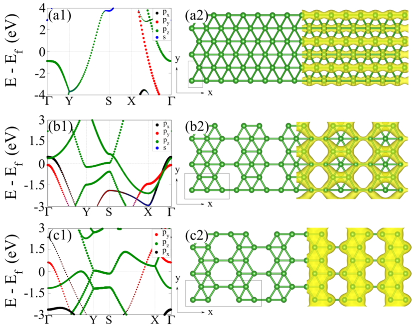
In Fig. 1 we present the structural models and the electronic bands structures of pristine borophene S0 [Fig. 1(a)], S1 [Fig. 1(b)], and S2 [Fig. 1(c)] phases. In S0 the B atoms are six-fold coordinated, and present a buckled geometry giving rise to two layers of boron atoms with a vertical distance ( direction) of 0.87 Å. The electronic band structure of S0 is highly anisotropic, characterized by the formation of metallic bands for wave vectors along the -X and Y-S directions [Fig. 1(a1)].Mannix et al. (2015) In Fig. 1(a2) we present projected the electronic density of states near the Fermi level, eV, where we can identify the wave function overlap along the -direction. Indeed, in a recent work, we verified that the electronic transport properties in S0 are characterized by a strong directional dependence.Padilha et al. (2016) Upon the presence of vacancies in S0, as observed in S1 and S2, the vertical buckling has been suppressed.Feng et al. (2016) The planar boron sheets, with four- five- and six-fold coordinated B atoms, are characterized by a density of hollow hexagons () Tang and Ismail-Beigi (2007) of 1/6 and 1/5, respectively.hol The energetic stability of those pristine systems was examined through the calculation of the cohesive energy ().Coh We found of 6.21, 6.25, and 6.27 eV/atom for S0, S1 and S2 phases. The energetic preference of S1 and S2, compared with S0 is in agreement with the previous first-principles results.Wu et al. (2012); Mannix et al. (2015); Feng et al. (2016)
The metallic character of borophene in S1 and S2 phases has been kept, Figs. 1(b1) and (c1), however, compared with S0, the electronic anisotropy is somewhat dimmed. We find that the metallic bands of S1 are mostly composed by the B-2 and -2 orbitals localized on the four- and five-fold coordinated B atoms. Meanwhile, in S2 the formation of the metallic bands along the -Y and S-X directions is dictated by a combination of - (B-) and -orbitals (B-).
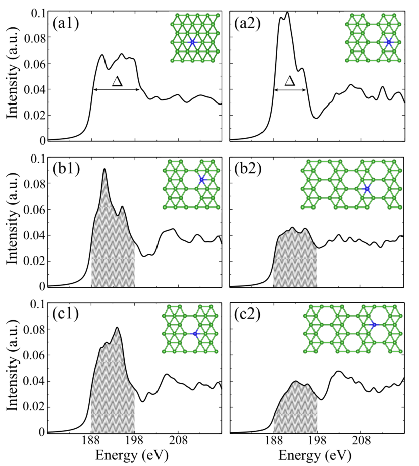
In order to get some insight into the structural and electronic features of the borophene sheets, we simulate the boron K-edge X-ray absorption near-edge structure (XANES). By considering the polarization vector perpendicular to the borophene sheet (), we have examined the main features associated with the B- transitions.
Boron atoms in S0, S1 and S2 are characterized by different bonding geometries and coordinations. (i) In S0 and S1 we have six-fold coordinated boron atoms. The former presents a buckled geometry, giving rise to boron lines along the -direction [Fig. 1(a2)], while S1 exhibits a planar geometry, where the six-fold boron atoms are separated by boron vacancy lines, Fig. 1(b2). As shown in Fig. 2(a1) and (a2), those structural differences can be identified at the near-edge absorption interval; namely, the B- absorption peak in S0 present a larger energy dispersion [ in Fig. 2(a1)] in comparison with its counterpart in S1 [Fig. 2(a2)]. Thus, indicating that the presence of vacancy lines, and the planar geometry of S1 result in a more localized states in comparison with the buckled S0 phase. At the atomic scale, we have a nice manifestation of the role played by the local geometry on the absorption spectra. In S0 the B–B bond length () between B atoms lying on the same layer, = 1.61 Å, is shorter than the ones of the six-fold coordinated boron atoms in S1 ( = 1.71 Å), and thus increasing the hybridizations in S0 in comparison with S1. (ii) S1 and S2 are planar structures, where we have vacancies, five-fold, and four-fold coordinated boron atoms. The former is characterized by hexagonal boron structures separated by vacancy lines, while in S2 we have zigzag rows of boron-dimers ( = 1.67 Å) separated by vacancy lines. As shown in Fig. 1(b2) and (c2), the electronic density of states of S1 and S2, near the Fermi level, present different features. The hybridization in S1 somewhat mimic the one present in graphene, while in S2 there is charge density overlap along the zigzag rows of B-dimers. Our simulated XANES results capture those structural and electronic differences. In S1, the near edge spectra [shaded regions in Fig. 2(b1) and (c1)] are characterized by a more intense and less dispersive B- transitions when compared with the ones in S2, [shaded regions in Figs. 2(b2) and (c2)]. Thus, indicating that the presence hexagonal (dimer) structures in S1 (S2) gives rise to a more (less) localized character of the orbitals near the Fermi level in S1 (S2).
Summarizing, firstly we have charaterized the structural and electronic properties of pristine S0, S1, and S2 borophene phases, and further XANES simulations revealed the connection between the local atomic structure, i.e. coordination and equilibrium geometry, and the X-ray absorption features. Those findings provide not only fingerprints for the different borophene structural phases, but also key insights into experimental measurements.
III.2 2D boron superlattices
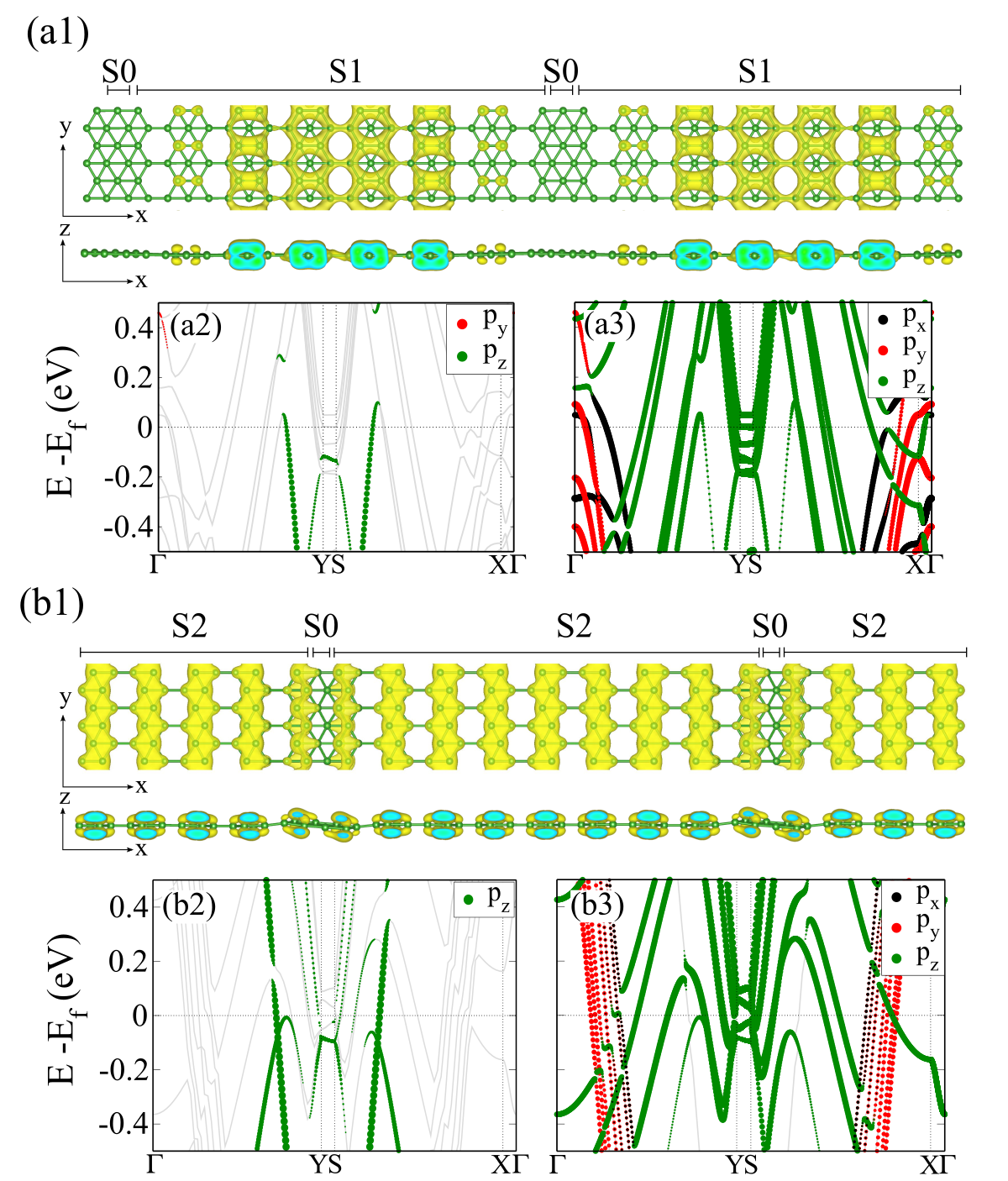
Motivated by the recent advances on the synthesis of 2D heterostructures,Liu et al. (2018) and the theoretically proposed electronic localization upon the presence of defects in borophene,Kistanov et al. (2018) we examined the structural and electronic properties of borophene lateral heterostructures. In particular, we have considered 2D borophene superlattices (BSLs) combining different structural phases of borophene, with m/n periodicities, separated by zigzag edges. For instance, in S01/S17 (m=1/n=7) we have one periodic unit cell of S0 separated by seven periodic unit cells of S1, Fig. 3(a1). It is worth noting that for such a lower proportion of S0, the vertical buckling in S0 has been suppressed. In S01/S17 the B–B bond length between the B atoms lying on the same (different) layer(s) increases (reduces) from 1.61 Å (1.87 Å) in pristine S0, to 1.83 Å (1.73 Å) at the inner sites of the S0 region. Similarly in S01/S24, Fig. 3(b1), where the vertical buckling at the inner sites of S0 reduces to 0.03 Å, with bond length between the B atoms lying on the same (different) layers(s) of 1.72 Å (1.70 Å). The energetic stability of those BSLs was inferred by the calculation of the cohesive energies (), where we found of 6.26 eV/atom. Our results of , summarized in Table I, show that the cohesive energies of the other BSLs are practically the same when compared with the ones of the pristine phases. Thus, supporting the energetic stability of those boron superlattices.
| S0m/S1n | ||||
|---|---|---|---|---|
| m/n | 1/7 | 2/6 | 3/5 | 4/4 |
| 6.26 | 6.25 | 6.25 | 6.23 | |
| S0m/S2n | ||||
| m/n | 2/4 | 2/2 | 4/1 | 8/1 |
| 6.27 | 6.27 | 6.23 | 6.23 | |
| S1m/S2n | ||||
| m/n | 4/1 | 2/1 | 2/2 | 1/4 |
| 6.26 | 6.27 | 6.27 | 6.27 | |
| m/n | 6/1 | 1/1 | 1/2 | 1/6 |
| 6.26 | 6.27 | 6.27 | 6.27 | |

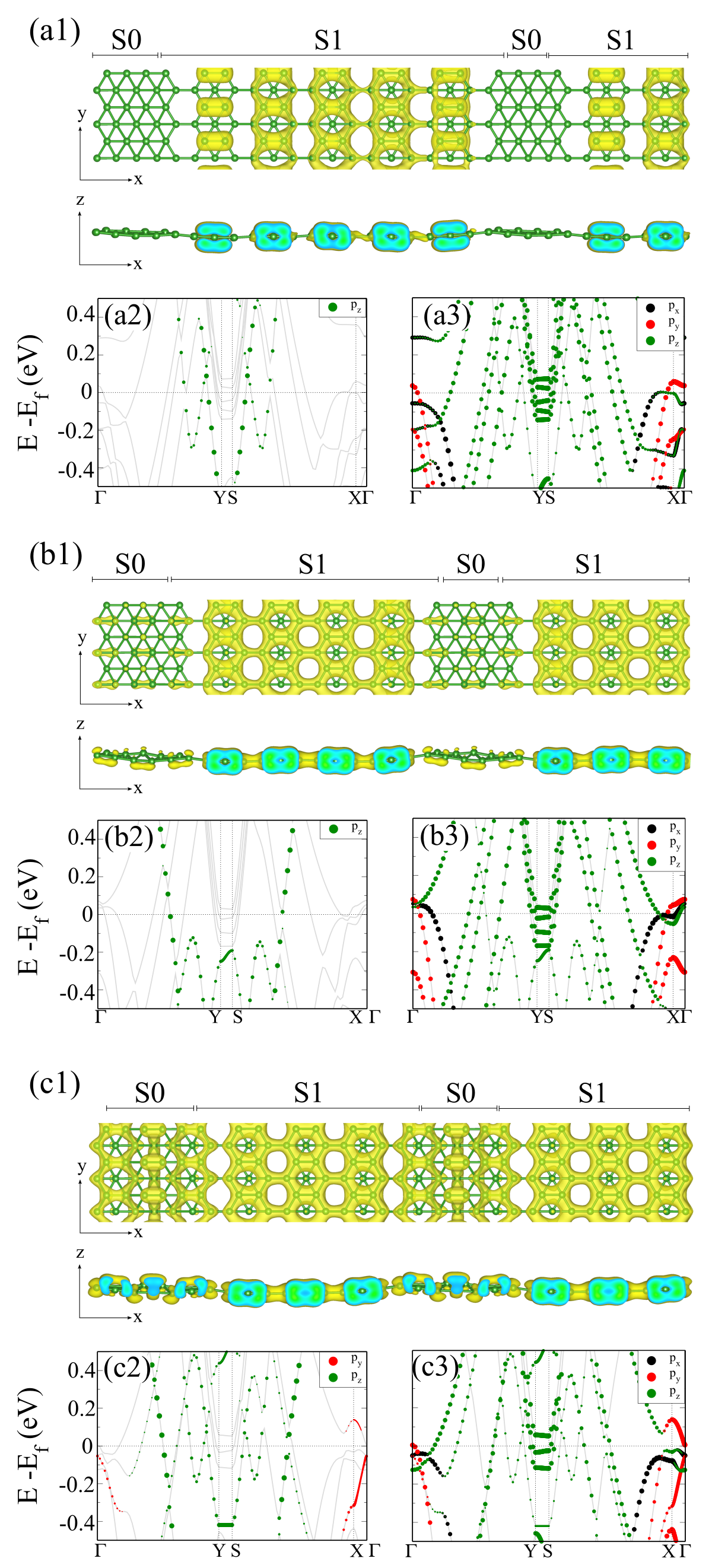
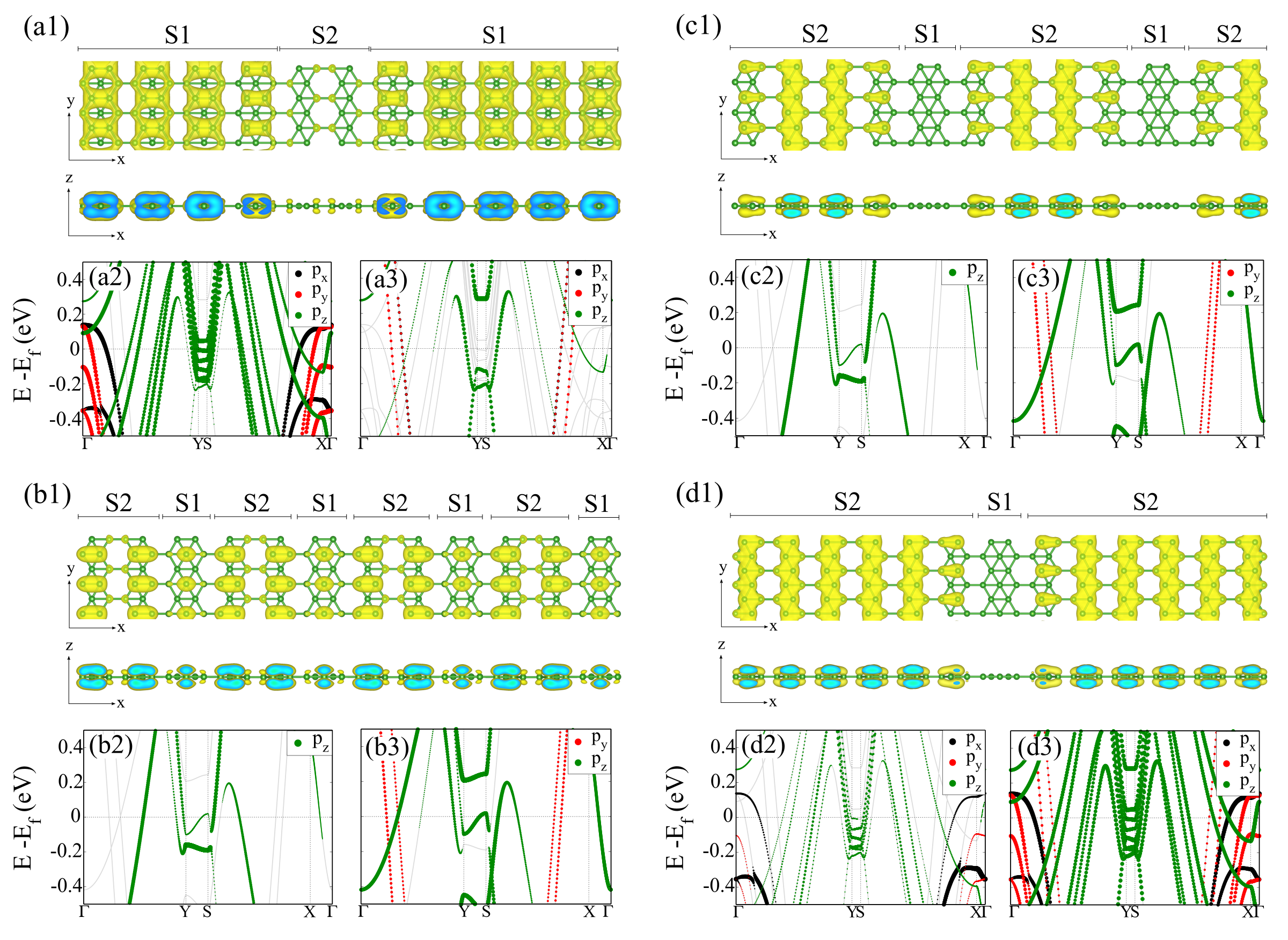
Next we examine the electronic properties of the BSLs as a function of the relative width (m/n) of each structural phase. In S01/S17 the electronic states near the Fermi level, eV, are mainly localized on S1 [Fig. 3(a1)], giving rise to electronic stripes composed by graphene-like -hybridizations along the four- and five-fold coordinated boron atoms, of the inner sites of S1, separated by S01 rows. The localization of the electronic states can be also identified through the projection of the energy bands on S0 and S1, Fig. 3(a2) and (a3), respectively; where it is noticeable the most of metallic bands lying on S1. Such a localization of the electronic states near the Fermi level, and the electronic separation of the metallic bands have been also observed in S02/S24, Fig. 3(b). Here, the electronic states are predominantly localized along the S2 region. However, as shown in Fig. 3(b3), in addition to the orbitals, we find that the -hybridizations also contribute to the formation of the metallic bands. The localization of the electronic states in the other S0m/S1n and S0m/S2n combinations, indicated in Table 1, are presented in the Appendix, Figs. 8 and 9.
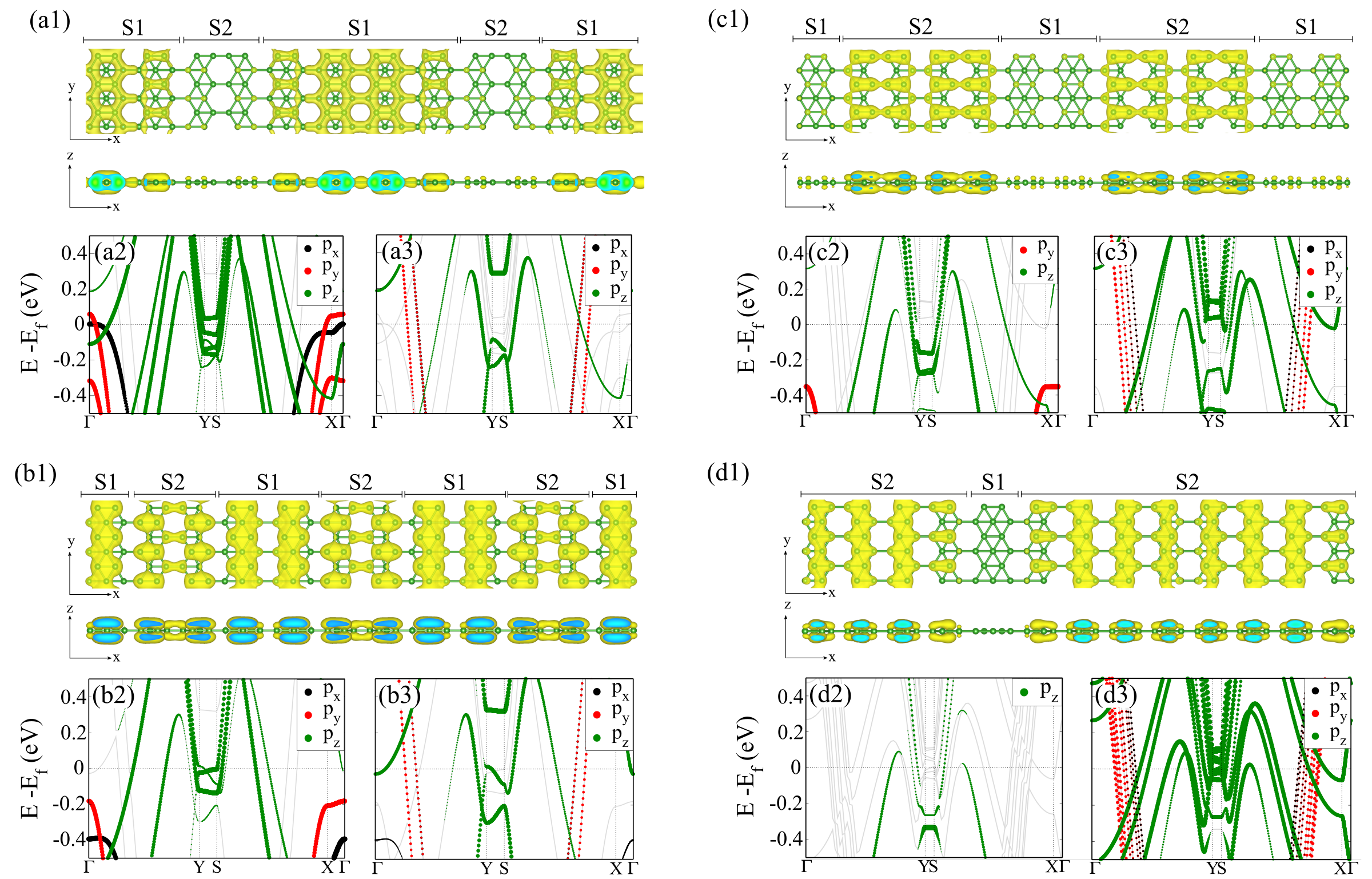
The large number of possible structural combinations to build up heterostructures, based on borophene, is a interesting degree of freedom in order to control/design the electronic properties in 2D systems. Very recently, borophene heterostructures composed by S1 and S2 phases have been successfully synthesized,Liu et al. (2018) where the authors identified S1/S2 periodic assemblies with different relative concentrations. Here we will examine the S1m/S2n BSLs, with m/n of 4/1, 2/1, 2/2, and 1/4, depicted in Fig. 4. At the equilibrium geometry, (i) the planar structure has been preserved, and (ii) the S1/S2 zigzag interface boron atoms are neatly arranged, where the B–B bond lengths and angles are practically the same compared with the ones the pristine structures. Indeed, at the equilibrium geometry, the bond lengths and angles at the interface region changes by less than 0.8% and 1.5%, respectively, compared with the ones of the pristine S1 and S2 phases. Thus, indicating that S1/S2 interfaces present lower strain than in S0/S1 and S0/S2.
In S14/S21, the electronic states within eV are mostly confined in S1 ruled by S2, Fig. 4(a1). There is a charge density overlap along S1, giving rise to metallic bands for wave vectors parallel to the Y and SX directions, Fig. 4(a2) and (a3). Those metallic bands are predominantly composed by B- orbitals lying on the four- and five-fold coordinated boron atoms of S1. Meanwhile, the projection of the energy bands on S2 reveals contributions from B- and - orbitals to the formation of the metallic bands. On the other hand, the electronic states with wave vector perpendicular to the S1/S2 interface, namely X and YS directions, are characterized by dispersionless energy bands localized mainly on S1. The localization of the electronic states on the other S1m/S2n BSLs, m/n = 6/1, 1/1, 1/2, and 1/6 (Table 1) are presented in the Appendix [Fig. 10], where we confirm the formation of tuneable electronic stripes in S1/S2 BSLs.
Reducing the width of S1, S14/S21 S12/S21, the distribution of the electronic density of states near the Fermi level, on S1 and S2, becomes almost equivalent, however they present different features, Fig. 4(b1). The metallic bands are characterized by -hybridization through S1, while in S2 we have both, i.e. - and -hybridizations (B-), with a major contribution from the latter along the zigzag B-dimers lines. Keeping the width of S1, and increasing S2, S12/S21 S12/S22, we find that the electronic states near the Fermi level become more localized on S2, mostly on the four-fold coordinated boron atoms, as shown in Fig 4(c1). Indeed, the -and -hybridizations along the S2 rows have been strengthened, giving rise to metallic bands along the Y and SX directions, concomitantly there is a reduction of the electronic contribution from S1. Finally, upon further reduction of S1 and increase of S2, S12/S22 S11/S24 [Fig. 4(d)], there is a noticeable change on the electronic distribution along S2, where the wave function overlap between the B- orbitals becomes more intense, strengthening the -hybridizations and the orbital localization along S2, characterized by zigzag rows of B-dimers. It is worth noting that the B-dimer bond length in S24 ( = 1.67 Å) is the same compared with that of S2 pristine.
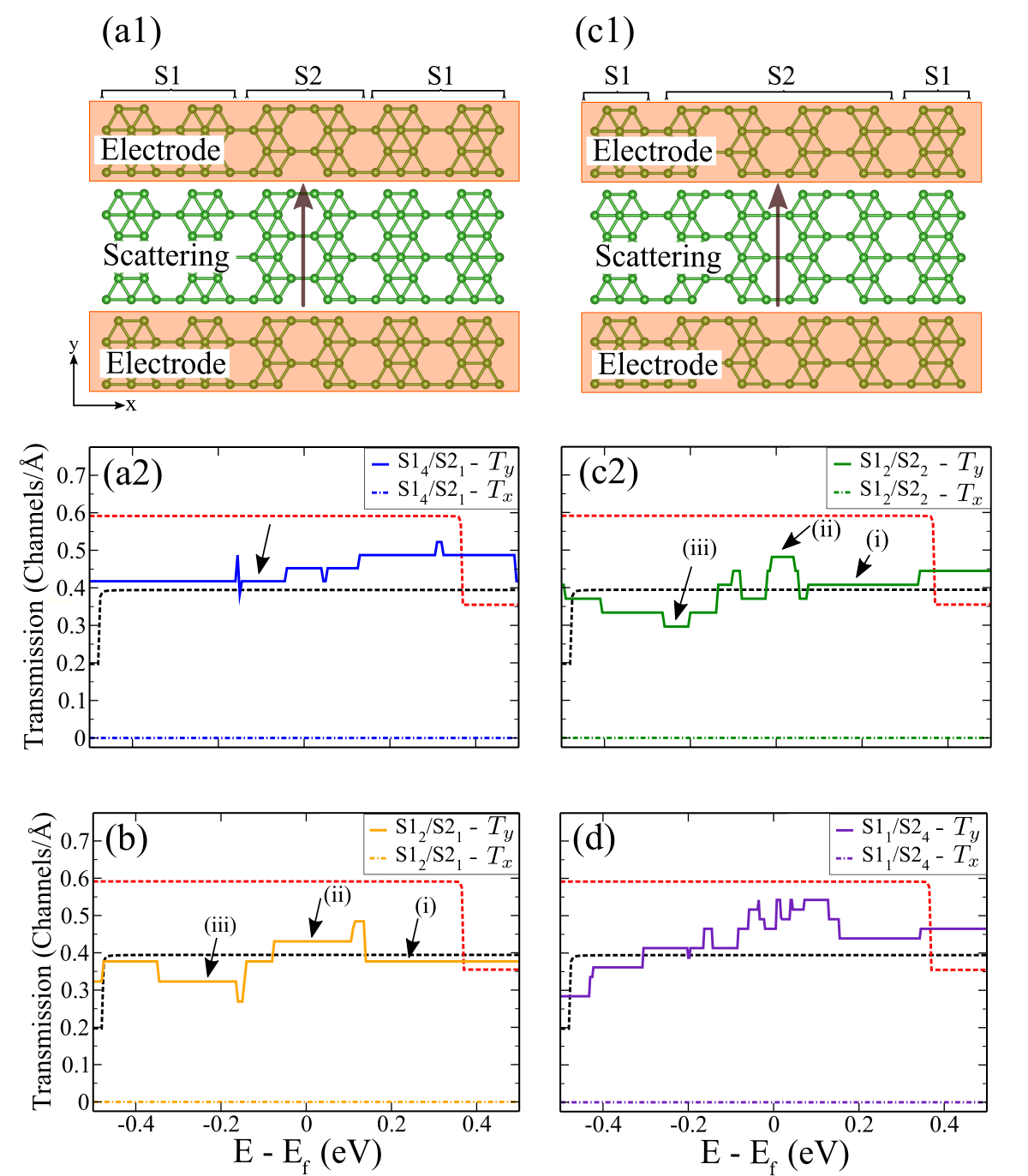
Focusing on the electronic transport properties in 2D systems, its “directional dependence”, and the “role of intrinsic line defects” are important issues that have been addressed in recent studies.Padilha et al. (2016); Shukla et al. (2018); Zeng and Chen (2019); Sivaraman et al. (2016) Here, we discuss the role of the electronic confinement on the transport properties along the BSLs S0/S1, S0/S2 [Fig. 3] and S1/S2 [Fig. 4]. We have examined the electronic transport along the superlattices, i.e. along the -direction. Perpendicularly to the interface, -direction, we obtained nearly zero transmission probabilities, thus indicating that the electronic transport in BSLS presents a strong directional dependence.
In Fig. 5(a1) and (b1) we present the setup used for the electronic transport calculations in S01/S17 and S02/S24. Our results of transmission probability () along the -direction of S01/S17 () and S02/S24 (), Fig. 5(a2) and (b2), reveal that near the Fermi level the transmission probabilities of the BSLs are lower when compared with those of the pristine phases, viz.: and . Such a reduction of the is due to the formation of localized states, characterized by the dispersionless energy bands along the YS directions [Fig. 3(a3) and (b3)] upon the formation of S0/S1 and S0/S2 interfaces. That is, there is an interaction between the propagating waves and the electronic states with wave vectors along the YS direction. Meanwhile, as shown Fig. 5(a2) and (b2), the transmission probabilities along the direction, that is, perpendicularly to the electronic stripes of S01/S17 and S02/S24 are nearly zero.
Our electronic transport results for the S1/S2 BSLs are summarized in Fig. 6. The simulation setups used for the calculation of in S14/S21 () and S12/S22 () are shown in Fig. 6(a1) and (c1), respectively. We find that lies between the transmission probabilities of pristine S1 () and S2 () phases, namely , for an energy interval of eV [Fig. 6(a2)]. Based upon the projected energy bands, Figs. 4(a2) and (a3), we can infer that the larger values of , compared with , can be attributed to the strengthening of the -hybridization along the inner sites of S1 and the presence metallic bands along S2, note that . On the other hand, the reduction of below the Fermi level, indicated by an arrow in Fig. 6(a2), is correlated with the formation of localized (B-) occupied states with wave vectors along the YS direction [Fig. 4(a2) and (a3)] just below the Fermi level.
By reducing the width of S1, S14/S21 S12/S21, we find (i) a reduction of the transmission probability, namely , (ii) being larger than only near the Fermi level [(i) and (ii) are indicated in Fig. 6(b)]. In fact, these features are in agreement with the reduction on the density of (B-) metallic bands along S1, as shown in Fig. 4(b). Meanwhile, the presence of localized states along the YS direction gives rise to the transmission valley below the Fermi level, indicate as (iii) in Fig. 6(b). Increasing the width of the S2 region, S12/S21 S12/S22, the features (i)–(iii) described above are are somewhat preserved. However, in S12/S22 the contribution of B- orbitals, localized on S2, becomes dominant to the formation of transport channels [Fig. 4(c2)]. That is, -channels start to rule the transmission probabilities. Upon further reduction (increase) of S1 (S2), S11/S24, there is an increase on the transmission probability near the Fermi level, but now dictated by the - and -channels along S2, Fig. 6(d), which is in agreement with the wave function overlap shown in Fig 4(d).
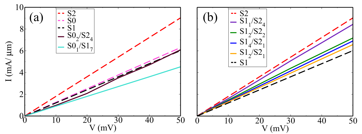
Finally, based on the Landauer formula we calculate the current density () as a function of the bias voltage () for the pristine S0, S1, and S2 phases (, , and , respectively), and the BSLs. The curves of those systems are characterized by a nearly linear behavior, Fig. 7. Among the pristine phases, S2 (S1) presents the higher (lower) current density. It is noticeable that the current densities of S01/S17 () and S02/S24 () are lower compared with the ones of the pristine phases, Fig. 7(a); whereas in S1/S2 BSLs we find the current densities lying between and , Fig. 7(b). The latter result can be attributed to the formation of neat interface structure between S1 and S2; while in the former there is a strengthening of the scattering processes which can be attributed to the large atomic distortions at the S0/S1 and S0/S2 interfaces.
IV Summary and Conclusions
Based on first-principles DFT calculations we have studied the electronic and structural properties of recently synthesized pristine borophene sheets with different vacancy concentrations, and borophene superlattices (BSLs) composed by combinations of borophene layers with different structural phases. Once we confirmed the metallic character of the pristine systems, through simulations of X-ray Absorption Near-Edge Structure (XANES) we unveil the connection between the electronic properties and the atomic arrangement of borophene S0, S1, and S2 phases. We found that each structural phase present a particular K-edge X-ray absorption spectrum, and thus, well defined XAS fingerprints. Electronic structure calculations reveal confinement effects, giving rise to metallic electronic stripes embedded in BSLs. Further electronic transport calculation reveals a strong directional dependence, where we found that the transmission probabilities and the formation of the transport channels are tuned by the m/n periodicity of the BSL. Such a tunning of the electronic confinement and transport properties offer a new and interesting set of degree of freedom addressing the design electronic nanoelectronic devices on 2D platforms.
IV.1 Appendix
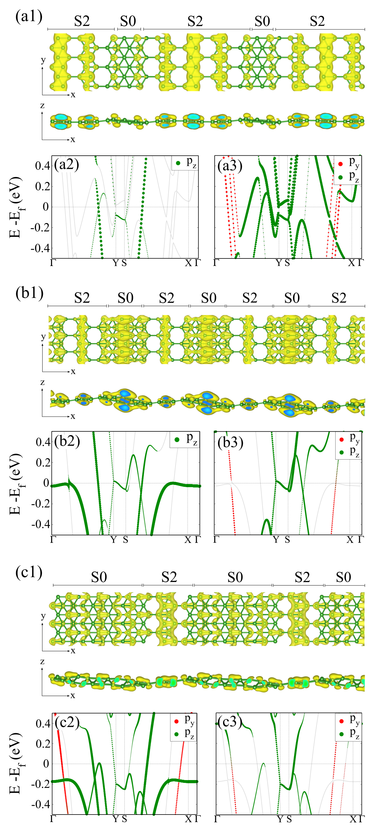
In Figs. 8(a1)-(c1) we present the localization of the electronic states near the Fermi level, eV, of S0m/S1n for m/n = 2/6, 3/5, and 4/4. There is an increase of the vertical buckling along the BSL proportional to the area of the S0 region. However, the localization of the metallic bands along the S1 region (mostly due to the B- orbitals) has been kept [Figs. 8(a2)-(b2) and 8(a3)-(b3)], although somewhat dimmed by increasing the proportion of S0. Similarly features have been found in S02/S22, where the surface area of S22 is larger in comparison with that of S02. On the other hand, the localization of the electronic states on S0 increases by increasing it area, Fig. 9. In Fig. 10 we present the electronic band structure, and the projection of the electronic states near the Fermi level for the S1m/S2n BSLs, with m/n = 6/1, 1/1, 1/2, and 1/6, where it is noticeable the change on the localization of the electronic states near the Fermi level, namely from S1 in S16/S21 [Fig. 10(a)] to S2 in S11/S26 [Fig. 10(d)].
Acknowledgements
The authors acknowledge financial support from the Brazilian agencies CNPq, and FAPEMIG, FAPES and the LNCC (SCAFMat2), CENAPAD-SP for computer time.
References
- Novoselov et al. (2004) K. S. Novoselov, A. K. Geim, S. V. Morozov, D. Jiang, Y. Zhang, S. V. Dubonos, I. V. Grigorieva, and A. A. Firsov, science 306, 666 (2004).
- Kunstmann and Quandt (2006) J. Kunstmann and A. Quandt, Physical Review B 74, 035413 (2006).
- Tang and Ismail-Beigi (2007) H. Tang and S. Ismail-Beigi, Physical review letters 99, 115501 (2007).
- Penev et al. (2012) E. S. Penev, S. Bhowmick, A. Sadrzadeh, and B. I. Yakobson, Nano letters 12, 2441 (2012).
- Wu et al. (2012) X. Wu, J. Dai, Y. Zhao, Z. Zhuo, J. Yang, and X. C. Zeng, ACS nano 6, 7443 (2012).
- Xu et al. (2018) S.-G. Xu, X.-T. Li, Y.-J. Zhao, J.-H. Liao, H. Xu, and X.-B. Yang, Nanoscale 10, 13410 (2018).
- Mannix et al. (2015) A. J. Mannix, X.-F. Zhou, B. Kiraly, J. D. Wood, D. Alducin, B. D. Myers, X. Liu, B. L. Fisher, U. Santiago, J. R. Guest, et al., Science 350, 1513 (2015).
- Feng et al. (2016) B. Feng, J. Zhang, Q. Zhong, W. Li, S. Li, H. Li, P. Cheng, S. Meng, L. Chen, and K. Wu, Nature Chemistry 8, 563 (2016).
- Ranjan et al. (2019) P. Ranjan, T. K. Sahu, R. Bhushan, S. S. Yamijala, D. J. Late, P. Kumar, and A. Vinu, Advanced Materials , 1900353 (2019).
- Zhang et al. (2016) X. Zhang, J. Hu, Y. Cheng, H. Y. Yang, Y. Yao, and S. A. Yang, Nanoscale 8, 15340 (2016).
- Jiang et al. (2016) H. Jiang, Z. Lu, M. Wu, F. Ciucci, and T. Zhao, Nano Energy 23, 97 (2016).
- Esaki and Tsu (1970) L. Esaki and R. Tsu, IBM Journal of Research and Development 14, 61 (1970).
- Bylander and Kleinman (1987) D. Bylander and L. Kleinman, Physical Review B 36, 3229 (1987).
- Hsu et al. (1994) Y. Hsu, W. Wang, and T. Kuan, Physical Review B 50, 4973 (1994).
- Gong et al. (2014) Y. Gong, J. Lin, X. Wang, G. Shi, S. Lei, Z. Lin, X. Zou, G. Ye, R. Vajtai, B. I. Yakobson, et al., Nature Materials 13, 1135 (2014).
- Huang et al. (2014) C. Huang, S. Wu, A. M. Sanchez, J. J. Peters, R. Beanland, J. S. Ross, P. Rivera, W. Yao, D. H. Cobden, and X. Xu, Nature Materials 13, 1096 (2014).
- Zhang et al. (2014) X.-Q. Zhang, C.-H. Lin, Y.-W. Tseng, K.-H. Huang, and Y.-H. Lee, Nano Letters 15, 410 (2014).
- Yoo et al. (2015) Y. Yoo, Z. P. Degregorio, and J. E. Johns, Journal of the American Chemical Society 137, 14281 (2015).
- Chen et al. (2015) K. Chen, X. Wan, J. Wen, W. Xie, Z. Kang, X. Zeng, H. Chen, and J.-B. Xu, ACS nano 9, 9868 (2015).
- Eda et al. (2011) G. Eda, H. Yamaguchi, D. Voiry, T. Fujita, M. Chen, and M. Chhowalla, Nano letters 11, 5111 (2011).
- Eda et al. (2012) G. Eda, T. Fujita, H. Yamaguchi, D. Voiry, M. Chen, and M. Chhowalla, Acs Nano 6, 7311 (2012).
- Liu et al. (2018) X. Liu, Z. Zhang, L. Wang, B. I. Yakobson, and M. C. Hersam, Nat. Mater 17, 783 (2018).
- Padilha et al. (2016) J. E. Padilha, R. H. Miwa, and A. Fazzio, Physical Chemistry Chemical Physics 18, 25491 (2016).
- Peng et al. (2016) B. Peng, H. Zhang, H. Shao, Y. Xu, R. Zhang, and H. Zhu, Journal of Materials Chemistry C 4, 3592 (2016).
- Zeng and Chen (2019) J. Zeng and K. Chen, The Journal of Physical Chemistry C (2019).
- Büttiker et al. (1985) M. Büttiker, Y. Imry, R. Landauer, and S. Pinhas, Phys. Rev. B 31, 6207 (1985).
- Meir and Wingreen (1985) Y. Meir and N. S. Wingreen, Phys. Rev. Lett. 31, 805 (1985).
- Perdew et al. (1996) J. P. Perdew, K. Burke, and M. Ernzerhof, Phys. Rev. Lett. 77, 3865 (1996).
- Kresse and Furthmller (1996a) G. Kresse and J. Furthmller, Comput. Mater. Sci. 6, 15 (1996a).
- Kresse and Furthmller (1996b) G. Kresse and J. Furthmller, Phys. Rev. B 54, 11169 (1996b).
- Monkhorst and Pack (1976) H. J. Monkhorst and J. D. Pack, Phys. Rev. B 13, 5188 (1976).
- Blchl (1994) P. E. Blchl, Phys. Rev. B 50, 17953 (1994).
- Bunău and Calandra (2013) O. Bunău and M. Calandra, Phys. Rev. B 87, 205105 (2013).
- Gougoussis et al. (2009) C. Gougoussis, M. Calandra, A. P. Seitsonen, and F. Mauri, Phys. Rev. B 80, 075102 (2009).
- Taillefumier et al. (2002) M. Taillefumier, D. Cabaret, A.-M. Flank, and F. Mauri, Phys. Rev. B 66, 195107 (2002).
- Giannozzi et al. (2009) P. Giannozzi et al., J. Phys.: Condens. Matter 21, 395502 (2009).
- Pickard and Mauri (2001) C. J. Pickard and F. Mauri, Physical Review B 63, 245101 (2001).
- Soler et al. (2002) J. M. Soler, E. Artacho, J. D. Gale, A. García, J. Junquera, P. Ordejón, and D. Sánchez-Portal, J. Phys.: Condens. Matter 14, 2745 (2002).
- Brandbyge et al. (2002) M. Brandbyge, J.-L. Mozos, P. Ordejón, J. Taylor, and K. Stokbro, Phys. Rev. B 65, 165401 (2002).
- Artacho et al. (1999) E. Artacho, D. Sánchez-Portal, P. Ordejón, A. Garcia, and J. M. Soler, Phys. Status Solid B 215, 809 (1999).
- (41) Within the SIESTA code, the cutoff radius of the basis set (pseudoatomic orbitals) can be tuned by a single parameter, energy shift. For lower energy shift we have larger cutoff radii for the atomic orbitals, that is, the basis set has been improved. In the present work we have considered an energy shift of 0.10 eV to determine the radius cutoff of the pseudoatomic orbitals. Here we verify the convergence of our total energy results for an energy shift of 0.05 eV.
- Landauer et al. (1988) R. Landauer, Y. Imry, M. Büttiker, and S. Pinhas, IBM Journal of Research and Development 32, 306 (1988).
- (43) Hole density () is defined as the ratio between the number of hexagon holes and the total number of atoms in the original (pristine) triangular lattice Tang and Ismail-Beigi (2007).
- (44) is defined as the total energy difference between the borophene sheet or superlattice and the isolated B atoms.
- Kistanov et al. (2018) A. A. Kistanov, Y. Cai, K. Zhou, N. Srikanth, S. V. Dmitriev, and Y.-W. Zhang, Nanoscale 10, 1403 (2018).
- Shukla et al. (2018) V. Shukla, A. Grigoriev, N. K. Jena, and R. Ahuja, Physical Chemistry Chemical Physics 20, 22952 (2018).
- Sivaraman et al. (2016) G. Sivaraman, F. A. de Souza, R. G. Amorim, W. L. Scopel, M. Fyta, and R. H. Scheicher, The Journal of Physical Chemistry C 120, 23389 (2016).