Hard superconducting gap and diffusion-induced superconductors in Ge-Si nanowires
Abstract
We show a hard superconducting gap in a Ge-Si nanowire Josephson transistor up to in-plane magnetic fields of mT, an important step towards creating and detecting Majorana zero modes in this system. A hard gap requires a highly homogeneous tunneling heterointerface between the superconducting contacts and the semiconducting nanowire. This is realized by annealing devices at ∘C during which aluminium inter-diffuses and replaces the germanium in a section of the nanowire. Next to Al, we find a superconductor with lower critical temperature ( K) and a higher critical field ( T). We can therefore selectively switch either superconductor to the normal state by tuning the temperature and the magnetic field and observe that the additional superconductor induces a proximity supercurrent in the semiconducting part of the nanowire even when the Al is in the normal state. In another device where the diffusion of Al rendered the nanowire completely metallic, a superconductor with a much higher critical temperature ( K) and critical field ( T) is found. The small size of these diffusion-induced superconductors inside nanowires may be of special interest for applications requiring high magnetic fields in arbitrary direction.
I Introduction
The discovery that Majorana fermions offer a route towards an inherently topologically protected fault-tolerant quantum computer Read and Green (2000); Das Sarma et al. (2005); Nayak et al. (2008) marked the beginning of a quickly growing field of research to achieve their experimental realization. Majorana fermions require a topological superconducting material, which in practice can be realized by coupling a conventional -wave superconductor to a 1-dimensional nanowire with high spin-orbit coupling and -factor Kitaev (2001); Oreg et al. (2010); Lutchyn et al. (2010, 2018). Signatures of Majorana fermions are expected to arise as a conductance peak at zero bias and finite magnetic fields. The first reports showing these zero-bias conductance peaks in InAs and InSb nanowires Das et al. (2012); Mourik et al. (2012); Deng et al. (2012); Lee et al. (2012); Finck et al. (2013); Churchill et al. (2013); Deng et al. (2015) suffered from sizeable sub-gap conductivity attributed to inhomogeneities in the nanowire-superconductor interface Takei et al. (2013); Cole et al. (2015). The resulting quasiparticle poisoning decoheres Majorana states since they will participate in braiding operations Rainis and Loss (2012); Higginbotham et al. (2015); Albrecht et al. (2017), and additionally obscure the Majorana signatures at zero energy. Strong efforts have been made to improve these interfaces, i. e., induce a hard gap, using epitaxially grown Al Chang et al. (2015); Kjaergaard et al. (2016) or specialized surface treatments methods Zhang et al. (2017); Gül et al. (2017), resulting in a much better resolved Majorana signatures Higginbotham et al. (2015); Albrecht et al. (2016); Deng et al. (2016); Gül et al. (2018).
In contrast to the group III-V materials used in most previous work, we use Ge-Si core-shell nanowires consisting of a mono-crystalline Ge core with a diameter of nm, and a Si shell thickness of nm covered by a native SiO2. Coherent strain in the defect-free crystal structure results in high hole-mobilities Conesa-Boj et al. (2017). The electronic properties of the one-dimensional hole gas localized in the Ge core Lu et al. (2005); Zhang et al. (2010) makes them a candidate for observing Majorana fermions Maier et al. (2014a); Thakurathi et al. (2017), and their interaction with a superconductor is still relatively unexplored Xiang et al. (2006); Su et al. (2016); Ridderbos et al. (2018); de Vries et al. (2018); Ridderbos et al. (2019). These wires are predicted to have a strong first-order Rashba type spin-orbit coupling Kloeffel et al. (2011) which, together with the g-factor Maier et al. (2013); Brauns et al. (2016), is tunable by electric fields. Our devices consist of a nanowire channel with superconducting Al source and drain placed on an oxidized Si substrate (for more detailed information about the fabrication process see Supplementary Information SI 1). We focus on two devices where an essential thermal annealing process results in inter-diffusion between Al in the contacts and Ge in the nanowire channel. Device A is an electric-field tunable Josephson junction Ridderbos et al. (2018, 2019) as shown in Fig. 1a, while in device B the whole semiconducting nanowire channel has been metalized and we suspect Al has largely replaced the semiconductor.
The electric field dependence of Device A has already been extensively studied in Ref. Ridderbos et al. (2018), where the main result was the observation of two distinct regimes: a highly transparect regime with a near ideal product in accumulation, and a tunneling regime with few-hole occupancy where supercurrent only appears at the charge degeneracy points. In this work, we extend on this by investigating the magnetic field dependence of the transport properties in both regimes.
To gain insight into the microscopic properties of the superconductor-semiconductor interfaces, we start by investigating Device A using high-angle annular dark field (HAADF) - scanning transmission electron microscopy (STEM) in combination with energy-dispersive X-ray spectroscopy (EDX). We find strong indications that the additional superconductor, as well as the highly homogeneous superconductor-nanowire interface arises during the thermal annealing process where Al inter-diffuses with the material in the semiconducting nanowire. In the second part, we map the switching current as a function of critical field and critical temperature of device A and B, which clearly shows an additional superconducting phase in both devices. In the final part we investigate the hardness of the superconducting gap in the semiconducting nanowire of device A, by means of electronic transport measurements near depletion Gül et al. (2017); Chang et al. (2015) and observe that the conductance in the gap is suppressed by a factor .
II Al-Ge inter-diffusion
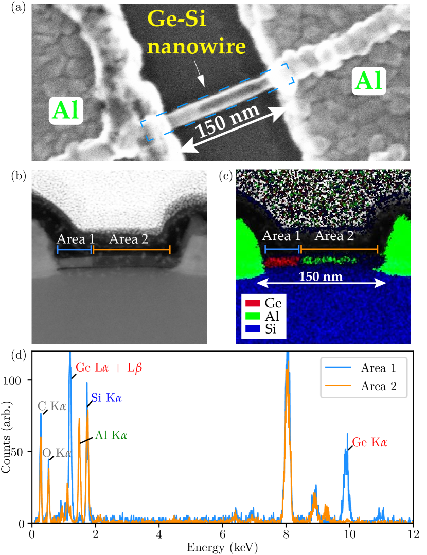
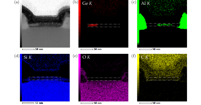
To investigate the effects of the annealing on the stoichiometric composition of the nanowire channel, a TEM lamella was made along the nanowire axes of device A as indicated in Figure 1a. We first apply a stack of protective SiO2 and Pt layers and subsequently create the TEM lamella using a standard focused ion beam lift-out protocol. This allows us to perform an analysis on the cross-section of the device as can be seen in Fig. 1b. In both Fig. 1a and b, a smaller region (Area 1) with higher contrast on the left, and a bigger region with lower contrast on the right (Area 2) can be observed. Fig. 1c shows the resulting EDX signals in these regions for the elements Ge, Si and Al and we observe a clear distinction: in Area 1 we observe a strong Ge signal while in Area 2 the signal is dominated by Al.
In Figure 1d we show the integrated EDX spectra for both areas. When comparing the two areas, we observe that in Area 2 the Ge , Ge and Ge signals fall below the detection limit. As is the convention in EDX analysis, and denote the orbital to which an electron decays in a picture where , , and are the outer atomic orbitals, while and indicate whether it decays from the first or second higher orbital. The Al signal shows the opposite behavior, implying that Ge has been replaced by Al in Area 2. The counts for elements O, C and Si remain equal in both areas (see also Supplementary Information Fig. S1). As we will discuss in the following section, the superconductor in Area 2 has profoundly different properties from the Al contacts and we therefore refer to it as X. Inter-diffusion has also taken place below the left contact without reaching the channel, although this is not evident from the TEM data. Instead, we conclude this from transport data in the next section (Fig. 2 and Supplementary Information Fig. S3). As a side-note, we cannot observe the effects of the inter-diffusion process on the Si shell, since the Si signal is dominated by the SiO2 that covers the substrate.
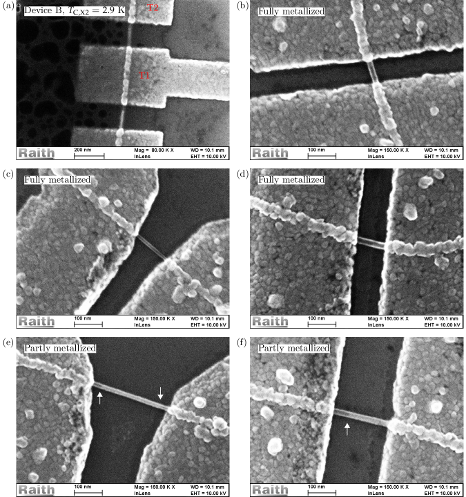
An in-depth study on the thermally induced inter-diffusion process between Al and pure Ge nanowires, a highly similar system to ours, has been performed in Refs. 40; 41. Here, in-situ monitoring of the metal front inside the nanowires at various temperatures reveals that the velocity of propagation as a function of the length of the metalized nanowire segment, is volume-diffusion limited, and possibly surface-diffusion limited, with the Al forming a mono-crystalline face-centered-cubic crystal inside the nanowire. The metal front forms an atomically sharp interface and no inter-metallic phase is found in the metalized nanowire segment, i.e., the Ge is transported out of the wire into the Al contacts. These observations are explained by a 15 orders of magnitude lower diffusion constant for Al in Ge than for Ge in Al Gale and Totemeier (2003); Villars and Cenzual (2012). Furthermore, the initial start of the diffusion reaction is governed by the respective activation energies ( kJ/mol for Ge in Al, kJ/mol Al in Ge Gale and Totemeier (2003); Villars and Cenzual (2012)) and may depend on the specific atomic arrangement of the initial nanowire-Al interface, explaining the variation in the starting time of the diffusion reaction, even for two separate contacts on the same wire. These findings largely correspond to our observations on Ge-Si core-shell nanowires and gives an explanation for the asymmetry in our contacts (see Supplementary Figure S2 for SEM images of partly and fully metalized nanowires) , as well as the variation in device properties.
III Two superconductors in a nanowire Josephson junction
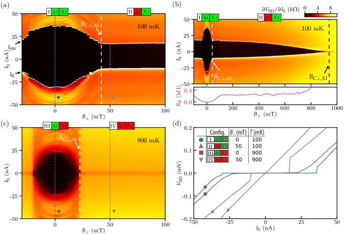
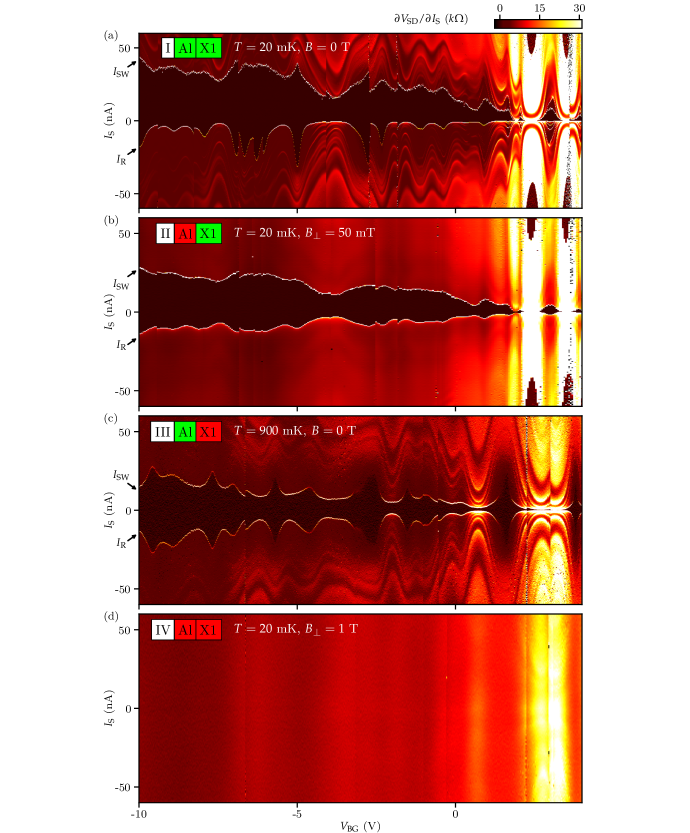
In Fig. 2a we show a magneto-spectroscopy of device A, the Josephson junction: we plot the differential resistance versus the sourced current and the out-of-plane magnetic field (see illustration in Fig. 3b) while sweeping from negative to positive current. The backgate is fixed at V where multiple subbands contribute to transport and the junction is highly transparent Ridderbos et al. (2018). The superconducting region (black) is bounded by with the retrapping current at negative bias and the switching current at positive bias. Upon increasing from , decreases gradually until aluminum becomes normal at the critical out-of-plane field mT after which a finite remains. For all , indicating that our junction is hysteretic for this particular value of due to the junction being underdamped Ridderbos et al. (2018) while additional heating-induced hysteresis can not be excluded Courtois et al. (2008) (see Supplementary Information Fig. S3a for a gate-dependence of and ).
When increasing further in Fig. 3b, slowly decreases and finally disappears. The proximity-induced supercurrent above implies the presence of a second superconducting material, X, in or near the nanowire channel with a critical field mT. To confirm that our Al contacts are normal for , we consider the background resistance in the superconducting region as a function of in the bottom panel of Fig. 2b. for , while for the background resistance gradually increases to k attributed to a normal series resistance of the Al contacts. Additionally, the out-of-plane critical field of a separately measured Al lead matches (see Supplementary Information Fig. S4).
In Fig 2c we show a magneto-spectroscopy at mK and observe that X is quenched for all , while Al still induces a supercurrent for mT. This shows that X has a lower and a higher than the Al contacts. Because X has a higher and a lower than Al, we can selectively switch either superconductor to the normal state, resulting in four possible device configurations I-IV as illustrated in Fig. 2 and summarized in the inset in Fig. 2d (a precise set of conditions for each configuration can be found in Supplementary Information Table S1). Fig. 2d shows plots of versus in all four configurations, clearly showing a supercurrent in configuration II where Al is normal and only X is superconducting. Since we observe a gate-tunable Josephson current even in configuration II, we conclude X is present on both sides of the Ge-Si segment (see Supplementary Information Fig. S3 for differential resistance maps versus backgate in all four configurations).
IV Junction versus and
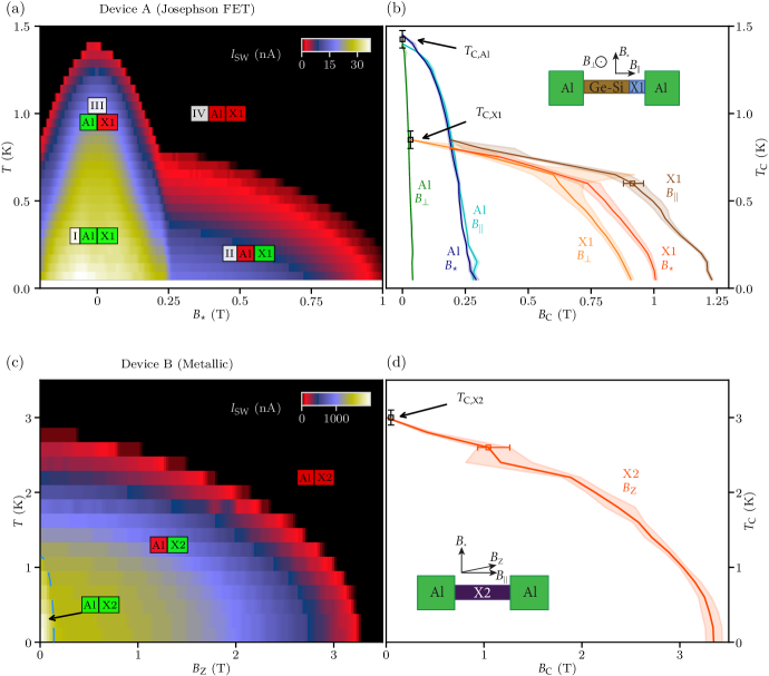
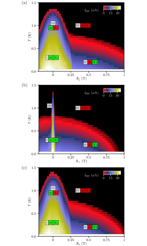
For the observed superconductors and their specific geometries, the critical field and critical temperature are inter-dependent variables and may have a non-trivial relation, the boundaries of the configurations I-IV in terms of and cannot directly be deduced from the data in Fig. 2. We therefore collect versus from magneto-spectroscopies for a large number of temperatures and the three main magnetic field axes , and which are illustrated by the inset in Fig. 3b. For the in-plane field perpendicular to the nanowire, has two clearly distinct overlapping shapes as a function of and in Fig. 3a: The ‘peak’ extending to mK at with a width of mT at mK is attributed to the superconducting state of Al, while the second shape (the ‘tail’), extending up to mT at mK, corresponds to the superconducting phase of X. We can thus map the four configurations in the color plot on the vs axes.
We now extract both the - and - curves from Fig. 3a (see Supplementary Information section SII), i. e., the critical temperature - critical field relation for Al and X, and plot them in Fig. 3b. We perform the same procedure for field directions and (see Supplementary Information Fig. S5 for versus and and ).
In Table. 1 we summarize the maximum , the resulting superconducting gap and in the three field directions for Al and X. Comparing mT with mT and mT we notice a factor ~ difference. This strong anisotropy for the out-of-plane field direction is clearly present in the - curves in Fig. 3b and is expected for the large aspect ratio of the 50 nm thick Al contacts.
The - curves show a less prominent magnetic field anisotropy from which we can roughly deduce the shape of X by assuming that the normal surface of the material is inversely proportional to the critical field, i. e., a larger superconducting normal-surface requires expelling more flux Tinkham (2004). Using the respective ratios of , and we observe that X is slightly elongated along the nanowire axis, reaffirming the hypothesis that X1 resides in the nanowire channel.
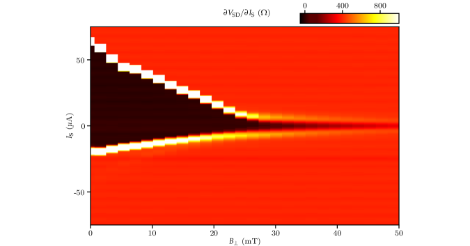
We now switch to the completely metalized device B where we believe Al has diffused completely through the channel, effectively making the nanowire a metallic superconductor. Fig. 3c shows vs and where the corresponding - relation in Fig. 3d is obtained by the previously mentioned polynomial fitting method. We see a critical temperature K at and critical field T at mK, both much higher than for X and the Al contacts. The switching current A is two orders of magnitude higher compared to device A.
When comparing K and T with thin Al aluminium films Meservey and Tedrow (1971), we observe X has equivalent properties of a nm thick film (in parallel field) and we could conclude that X is simply a very small cylinder of aluminium inside the nanowire channel. However, for X with K and T an equivalent film thickness cannot be defined. Even though no inter-metallic phases were found for annealed pure Ge nanowires in Refs. 40; 41, a possible origin of X is the formation of a Al-Si/Ge alloy in our core-shell nanowires, albeit with a ratio of semiconductor to Al below that of our EDX detection limit. In literature, certain stoichiometric compositions indeed result in a lower than for pure Al Deutscher and Rappaport (1979); Lesueur et al. (1988) and in fact, one can get alloys with a ranging from K up to K by various methods Deutscher et al. (1971); Tsuei and Johnson (1974); Kuan et al. (1982); Chevrier et al. (1987); Xi et al. (1987). The exact composition of both X and X in our Ge-Si core-shell system therefore remains partly speculative and would require a more in-depth study like Ref. 41.
To sum up, we observe X with K in a Josephson junction and X with K in a metallic device, showing that diffusion of Al into Ge-Si nanowires can gives rise to different superconductors with a lower and much higher than that of the Al contacts, both appear as a second superconductor in transport measurements.
V Tunneling regime of the Josephson FET
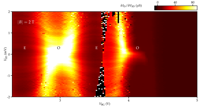
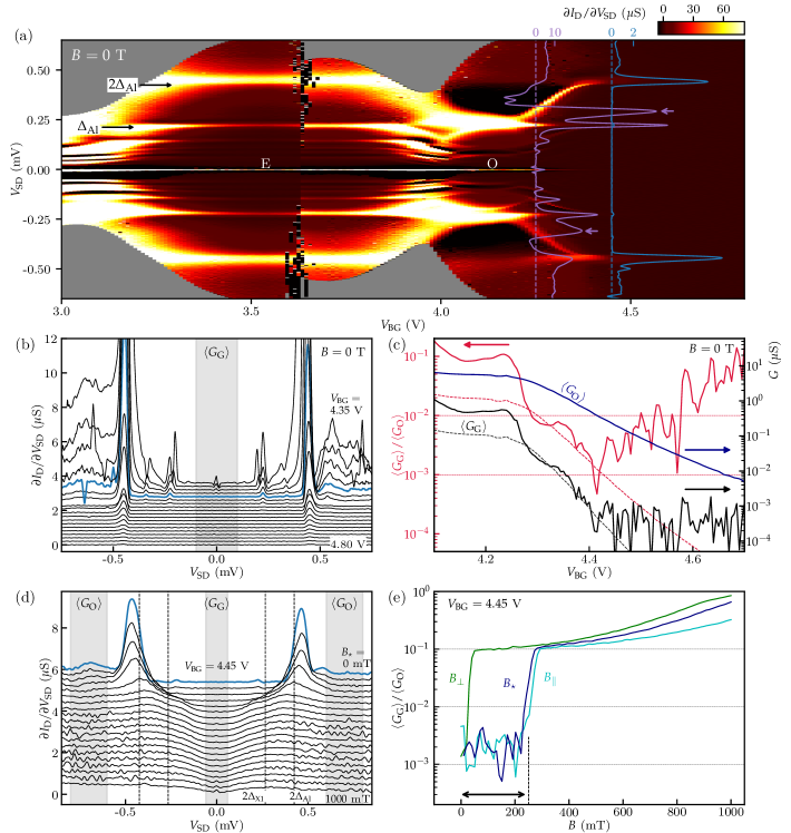
We now focus on device A and tune to a regime where the nanowire is near depletion. Fig. 4a shows the differential conductance versus the source-drain voltage and the backgate voltage . We notice a zero-bias conductance peak as the result of a finite Josephson current and a prominent multiple Andreev reflection (MAR) pattern showing as horizontal lines of increased conductance for to V. The reduced barrier transparency near depletion confines charges in the nanowire channel, and allows us to see odd and even charge occupation in a quantum dot in the wire Ridderbos et al. (2018) supported by a Kondo peak on the odd transitions Ridderbos et al. (2018); Kim et al. (2013) (see Supplementary Information, Fig. S6). Above V, the MAR and zero-bias peak disappear, while the onset of quasiparticle transport is visible at the superconducting gap at . This trend is also present in the linecuts for between and V in Fig. 4b.
In Fig. 4a between V and V we observe a conductance peak in both bias directions smoothly moving from to when going from the odd to the even occupancy, which we attribute to an Andreev bound state (ABS). Additional evidence for an ABS presents itself in the form of a region of negative differential conductance in the odd occupancy between and Pillet et al. (2010); Gramich et al. (2017), as highlighted by the purple linecut at V in Fig. 3a. Tunnel spectroscopy on an ABS requires asymmetric opaque tunnel barriers where the most opaque barrier probes the ABS Kim et al. (2013). A barrier asymmetry in our devices can indeed be expected, since the final interface properties are determined by microscopic details on the Al-nanowire interface during annealing. For lower our barriers quickly become highly transparent Ridderbos et al. (2018) and we therefore only observe the ABS signature near depletion.
In contrast to the bias-symmetric MAR features, the asymmetric barriers show up in the intensity of the ABS signatures (see the arrows on the purple linecut in Fig. 4a). Depending on the bias direction, there are two different rate-determining tunnel sequences: (1) tunneling through an opaque barrier onto a single ABS or (2) tunneling from an ABS through an opaque barrier into the Fermi sea. Sequence (2) has a much higher tunnel probability than (1), which results in the observed asymmetry in conductance.
VI Hard superconducting gap
A measure for the amount of quasiparticle states inside the gap, is the in-gap suppression of conductance also termed as the hardness of the gap. We therefore investigate the ratio where () is a conductance value inside (outside) the gap averaged over a range of as shown in Fig. 4b. is determined from a similar measurement at higher bias (see Fig. SI-7), sufficiently far away from . Fig. 4c shows , and the ratio versus and we find the conductance is suppressed by a factor for V, an order of magnitude higher than previously reported in this system in the same superconductor-normal-superconductor (SNS) configuration de Vries et al. (2018).
A SNS junction can naively be viewed as two superconductor-normal (SN) junctions in series and the theoretical dependence of on can therefore be approximated as Beenakker (1992):
| (1) |
and it follows that the equivalent conductance suppression of a SN device is a factor two lower than for a SNS device. We use the averaged as and obtain the theoretical minimal in-gap conductance , as well as the corresponding ratio , shown as dashed lines in Fig. 4c. We find that above V, the measured and closely follow the theoretical curves until the noise limit of our equipment is reached for V. This suggests that is not dominated by quasiparticle poisoning and that our superconductor-semiconductor interfaces do not facilitate inelastic scattering and have low disorder Takei et al. (2013). We note that for these values of , the Ge-Si island is not fully depleted ( still decreases as a function of and can be fully suppressed) and transport takes place through a tunnel-broadened quantum dot level (see also Ref. 34). However, the obtained theoretical minimal in-gap conductance should be considered an approximation since we do not take into account any difference in interface transparency between the two contacts.
When measured in a SNS configuration, the ratio gives an upper limit and could in reality be lower since it can be increased due to several other reasons than quasiparticle poisoning: (1) for higher , is limited by the noise floor of our measurement setup and does not further decrease. The decrease of now lowers the observed current suppression . (2) For lower , MAR and the zero-bias peak, both characteristic for Josephson junctions, appear as conductance peaks inside the gap which leads to a decreased (3) The quantum dot in the junction may lead to Fabry-Perot resonances and Kondo-enhanced tunnelling around zero bias (see Fig. SI-6). SN devices will not exhibit these effects and may therefore result in a lower ratio and give a better approximation of the quasiparticle density in the gap. Because of this, we cannot directly compare the current suppression in our device with other work probing the superconducting gap using a single superconducting contact. Nevertheless, the fact that our is limited by the noise floor our measurement setup suggests that our semiconductor-nanowire interface homogeneity could be comparable to InAs nanowire devices using epitaxial growth techniques Chang et al. (2015) or specialized surface treatments Gül et al. (2017).
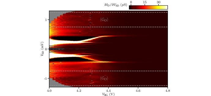
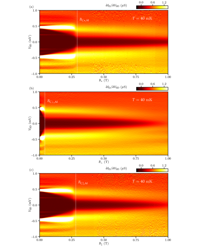
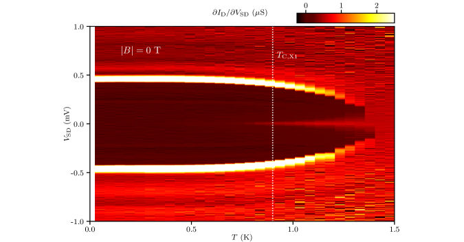
We will now look at the magnetic field dependence of the hardness of the gap. We fix at V and plot versus for several in Fig. 4d. For increasing , the sharp quasiparticle peak at reduces in height and broadens up to mT. Above , we enter configuration II where only X is superconducting but which fails to produce a clear second quasiparticle peak at . Instead, we see a ‘soft gap’ signature Takei et al. (2013) persisting up to which we attribute to X having an ill-defined gap due to possible diffusion-induced spatial variations in its stoichiometry or geometry.
In Fig 4e we plot the ratio for the three main field directions. The initial ratio is ~ in configuration I as defined in Fig. 2 and the gap remains hard until we approach the critical field of Al for the respective field direction as summarized in Table 1 (See Supplementary Information Fig. S8 for the corresponding differential conductance maps for all three main field axes). The highest field where the gap remains hard, mT, is slightly lower than because of the strongly reduced at this field. The much softer gap in configuration II induced by X leads to a which gradually increases to approaching .
Another example of the change in transport properties when Al becomes normal is seen in Fig. 2a and Fig. 2c. Here, the fringes in the normal state attributed to multiple Andreev reflections (MAR) are only visible for . For , the absence of MAR suggests an increase of inelastic processes due to an ill-defined induced gap or a greatly increased quasiparticle poisoning rate.
The results in Fig. 4e show that the Al contacts needs to be superconducting in order to observe a hard gap. On the other hand, when only Al is superconducting, i. e., going from configuration I to III we observed no change in that can be attributed to X becoming normal (see Supplementary Information, Fig. S9 for the temperature dependence of the differential conductance at V and ). This suggests that X does not need to be a superconductor to observe a hard gap as long as the Al contacts proximise the entire junction. This is likely to happen, since the transparency between Al and X is high, and indicating a coherence length for X comparable or larger than for Al, i. e., in the order of m Gross and Marx (2005).
Previously in this system a soft gap signature using NbTiN contacts has been shown Su et al. (2016), as well as hard gap using Al contacts de Vries et al. (2018). This work adds an investigation of the superconductor-semiconductor interfaces and their microscopic properties. We therefore revisit Fig. 1b and c and take a closer look at the interface between the X and the Ge-Si island. Even though our TEM and EDX resolution prohibits a conclusive statements about the interface properties on an atomic scale, the abrupt change in contrast suggests an upper limit for the interface width of a few nanometer. As explained, this observation is supported by Refs. 40; 41 showing an atomically sharp interface between the Ge and Al segment where both remain crystalline Kral et al. (2015); El Hajraoui et al. (2019). This type of interface would fit our observation of a hard gap, requiring a defect-free highly homogeneous heterointerface Takei et al. (2013) and low junction transparency close to depletion. This indicates that the inter-diffusion reaction between Ge and Al is essential for the observed hard superconducting gap Kral et al. (2015); El Hajraoui et al. (2019).
Utilizing these interfaces in devices suitable for measuring Majorana fermions in this system Maier et al. (2014b) would require a high level of control over the inter-diffusion process, i.e., lateral diffusion and metalization of nanowire segments should be prevented. One route would be to perform device annealing while in-situ monitoring of the diffusion process as in Ref. 41, or possibly a higher level of control could be achieved by optimizing the annealing process. In addition, one would require thinner Al leads in order to withstand the required in-plane magnetic fields ( T) to reach the topological phase transition Maier et al. (2013, 2014a).
With a controlled inter-diffusion reaction, the superconductors X and X themselves would also pose as interesting materials since their high in relation to their superconducting gaps, might allow the creation of Majorana fermions in materials where low g-factors could be limiting Stanescu and Tewari (2013). However, more research is required to understand the soft gap induced by X and to fully explore the possible superconductors, their composition, and formation process.
VII Conclusion
We have shown that Ge-Si nanowire devices with Al contacts contain additional superconductors after annealing, caused by diffusion of Al into the nanowire channel. We identify two superconductors in two different devices: X is present in a Josephson FET and X resides in a metallic nanowire channel. Both X and X remain superconducting for magnetic fields much higher than the Al contacts which could be of potential interest for applications where proximity-induced superconductivity is required in high magnetic fields.
Close to depletion, the Josephson FET exhibits a hard superconducting gap where the in-gap conductance is suppressed by a factor ~ in a SNS configuration where the in-gap conductance is close to the approximate theoretical minimum. The gap remains hard up to magnetic fields of mT. For higher fields, a soft gap remains up to the critical field of X. We can selectively switch Al or X from the normal to the superconducting state and, together with the TEM and EDX analysis, we believe that the diffusion-induced homogeneous heterointerface between the Ge core and the metalized nanowire segment is key in obtaining this hard gap. The next challenge is to more precisely control the diffusion of Al which would grant a highly promising system for observing Majorana zero modes Maier et al. (2014a).
VIII Acknowledgements
Acknowledgements.
The authors acknowledge financial support from the Netherlands Organization for Scientific Research (NWO). E.P.A.M.B. acknowledges financial support through the EC Seventh Framework Programme (FP7-ICT) initiative under Project SiSpin No. 323841. Solliance and the Dutch province of Noord-Brabant are acknowledged for funding the TEM facility. This project has received funding from the European Union’s Horizon 2020 research and innovation programme under Grant Agreement #862046.References
- Read and Green (2000) N. Read and D. Green, Physical Review B 61, 10267 (2000).
- Das Sarma et al. (2005) S. Das Sarma, M. Freedman, and C. Nayak, Physical Review Letters 94, 166802 (2005).
- Nayak et al. (2008) C. Nayak, S. H. Simon, A. Stern, M. Freedman, and S. Das Sarma, Reviews of Modern Physics 80, 1083 (2008).
- Kitaev (2001) A. Y. Kitaev, Physics-Uspekhi 44, 131 (2001).
- Oreg et al. (2010) Y. Oreg, G. Refael, and F. von Oppen, Physical Review Letters 105, 177002 (2010).
- Lutchyn et al. (2010) R. M. Lutchyn, J. D. Sau, and S. Das Sarma, Physical Review Letters 105, 077001 (2010).
- Lutchyn et al. (2018) R. M. Lutchyn, E. P. A. M. Bakkers, L. P. Kouwenhoven, P. Krogstrup, C. M. Marcus, and Y. Oreg, Nature Reviews Materials 3, 52 (2018).
- Das et al. (2012) A. Das, Y. Ronen, Y. Most, Y. Oreg, M. Heiblum, and H. Shtrikman, Nature Physics 8, 887 (2012).
- Mourik et al. (2012) V. Mourik, K. Zuo, S. M. Frolov, S. R. Plissard, E. P. A. M. Bakkers, and L. P. Kouwenhoven, Science 336, 1003 (2012).
- Deng et al. (2012) M. T. Deng, C. L. Yu, G. Y. Huang, M. Larsson, P. Caroff, and H. Q. Xu, Nano Letters 12, 6414 (2012).
- Lee et al. (2012) E. J. H. Lee, X. Jiang, R. Aguado, G. Katsaros, C. M. Lieber, and S. De Franceschi, Physical Review Letters 109, 186802 (2012).
- Finck et al. (2013) A. D. K. Finck, D. J. Van Harlingen, P. K. Mohseni, K. Jung, and X. Li, Physical Review Letters 110, 126406 (2013).
- Churchill et al. (2013) H. O. H. Churchill, V. Fatemi, K. Grove-Rasmussen, M. T. Deng, P. Caroff, H. Q. Xu, and C. M. Marcus, Physical Review B 87, 241401 (2013).
- Deng et al. (2015) M. T. Deng, C. L. Yu, G. Y. Huang, M. Larsson, P. Caroff, H. Q. Xu, P. Caroff, M. Larsson, G. Y. Huang, M. T. Deng, C. L. Yu, G. Y. Huang, M. Larsson, P. Caroff, and H. Q. Xu, Scientific Reports 4, 7261 (2015).
- Takei et al. (2013) S. Takei, B. M. Fregoso, H. Y. Hui, A. M. Lobos, and S. Das Sarma, Physical Review Letters 110, 186803 (2013).
- Cole et al. (2015) W. S. Cole, S. Das Sarma, and T. D. Stanescu, Physical Review B 92, 174511 (2015).
- Rainis and Loss (2012) D. Rainis and D. Loss, Physical Review B - Condensed Matter and Materials Physics 85, 1 (2012).
- Higginbotham et al. (2015) A. P. Higginbotham, S. M. Albrecht, G. Kiršanskas, W. Chang, F. Kuemmeth, P. Krogstrup, T. S. Jespersen, J. Nygård, K. Flensberg, and C. M. Marcus, Nature Physics 11, 1017 (2015).
- Albrecht et al. (2017) S. M. Albrecht, E. B. Hansen, A. P. Higginbotham, F. Kuemmeth, T. S. Jespersen, J. Nygård, P. Krogstrup, J. Danon, K. Flensberg, and C. M. Marcus, Physical Review Letters 118, 137701 (2017).
- Chang et al. (2015) W. Chang, S. M. Albrecht, T. S. Jespersen, F. Kuemmeth, P. Krogstrup, J. Nygård, and C. M. Marcus, Nature Nanotechnology 10, 232 (2015).
- Kjaergaard et al. (2016) M. Kjaergaard, F. Nichele, H. J. Suominen, M. P. Nowak, M. Wimmer, A. R. Akhmerov, J. A. Folk, K. Flensberg, J. Shabani, C. J. Palmstrøm, and C. M. Marcus, Nature Communications 7, 12841 (2016).
- Zhang et al. (2017) H. Zhang, Ö. Gül, S. Conesa-Boj, M. P. Nowak, M. Wimmer, K. Zuo, V. Mourik, F. K. de Vries, J. van Veen, M. W. A. de Moor, J. D. S. Bommer, D. J. van Woerkom, D. Car, S. R. Plissard, E. P. A. M. Bakkers, M. Quintero-Pérez, M. C. Cassidy, S. Koelling, S. Goswami, K. Watanabe, T. Taniguchi, and L. P. Kouwenhoven, Nature Communications 8, 16025 (2017).
- Gül et al. (2017) Ö. Gül, H. Zhang, F. K. de Vries, J. van Veen, K. Zuo, V. Mourik, S. Conesa-Boj, M. P. Nowak, D. J. van Woerkom, M. Quintero-Pérez, M. C. Cassidy, A. Geresdi, S. Koelling, D. Car, S. R. Plissard, E. P. A. M. Bakkers, and L. P. Kouwenhoven, Nano Letters 17, 2690 (2017).
- Albrecht et al. (2016) S. M. Albrecht, A. P. Higginbotham, M. Madsen, F. Kuemmeth, T. S. Jespersen, J. Nygård, P. Krogstrup, and C. M. Marcus, Nature 531, 206 (2016).
- Deng et al. (2016) M. T. Deng, S. Vaitiekėnas, E. B. Hansen, J. Danon, M. Leijnse, K. Flensberg, J. Nygård, P. Krogstrup, and C. M. Marcus, Science 354, 1557 (2016).
- Gül et al. (2018) Ö. Gül, H. Zhang, J. D. S. Bommer, M. W. A. de Moor, D. Car, S. R. Plissard, E. P. A. M. Bakkers, A. Geresdi, K. Watanabe, T. Taniguchi, and L. P. Kouwenhoven, Nature Nanotechnology 13, 192 (2018).
- Conesa-Boj et al. (2017) S. Conesa-Boj, A. Li, S. Koelling, M. Brauns, J. Ridderbos, T. T. Nguyen, M. A. Verheijen, P. M. Koenraad, F. A. Zwanenburg, and E. P. A. M. Bakkers, Nano Letters 17, 2259 (2017).
- Lu et al. (2005) W. Lu, J. Xiang, B. P. Timko, Y. Wu, and C. M. Lieber, Proceedings of the National Academy of Sciences 102, 10046 (2005).
- Zhang et al. (2010) S. Zhang, F. J. Lopez, J. K. Hyun, and L. J. Lauhon, Nano letters 10, 4483 (2010).
- Maier et al. (2014a) F. Maier, J. Klinovaja, and D. Loss, Physical Review B 90, 195421 (2014a).
- Thakurathi et al. (2017) M. Thakurathi, D. Loss, and J. Klinovaja, Physical Review B 95, 155407 (2017).
- Xiang et al. (2006) J. Xiang, A. Vidan, M. Tinkham, R. M. Westervelt, and C. M. Lieber, Nature Nanotechnology 1, 208 (2006).
- Su et al. (2016) Z. Su, A. Zarassi, B.-M. Nguyen, J. Yoo, S. A. Dayeh, and S. M. Frolov, arXiv:1610.03010 (2016).
- Ridderbos et al. (2018) J. Ridderbos, M. Brauns, J. Shen, F. K. de Vries, A. Li, E. P. A. M. Bakkers, A. Brinkman, and F. A. Zwanenburg, Advanced Materials 30, 1802257 (2018).
- de Vries et al. (2018) F. K. de Vries, J. Shen, R. J. Skolasinski, M. P. Nowak, D. Varjas, L. Wang, M. Wimmer, J. Ridderbos, F. A. Zwanenburg, A. Li, S. Koelling, M. A. Verheijen, E. P. A. M. Bakkers, and L. P. Kouwenhoven, Nano Letters 18, 6483 (2018).
- Ridderbos et al. (2019) J. Ridderbos, M. Brauns, A. Li, E. P. A. M. Bakkers, A. Brinkman, W. G. van der Wiel, and F. A. Zwanenburg, Physical Review Materials 3, 084803 (2019).
- Kloeffel et al. (2011) C. Kloeffel, M. Trif, and D. Loss, Physical Review B 84, 195314 (2011).
- Maier et al. (2013) F. Maier, C. Kloeffel, and D. Loss, Physical Review B 87, 161305 (2013).
- Brauns et al. (2016) M. Brauns, J. Ridderbos, A. Li, E. P. A. M. Bakkers, and F. A. Zwanenburg, Physical Review B 93, 121408(R) (2016).
- Kral et al. (2015) S. Kral, C. Zeiner, M. Stöger-Pollach, E. Bertagnolli, M. I. den Hertog, M. Lopez-Haro, E. Robin, K. El Hajraoui, and A. Lugstein, Nano Letters 15, 4783 (2015).
- El Hajraoui et al. (2019) K. El Hajraoui, M. A. Luong, E. Robin, F. Brunbauer, C. Zeiner, A. Lugstein, P. Gentile, J. L. Rouvière, and M. Den Hertog, Nano Letters 19, 2897 (2019).
- Gale and Totemeier (2003) W. F. Gale and T. C. Totemeier, Smithells Metals Reference Book 8th edition, edited by W. F. Gale. and T. C. Totemeier (Elsevier Ltd, 2003) p. 2080.
- Villars and Cenzual (2012) P. Villars and K. Cenzual, eds., Landolt-Börnstein - Group III Condensed Matter, Volume 43A11, Landolt-Börnstein - Group III Condensed Matter, Vol. 43A11 (Springer Berlin Heidelberg, Berlin, Heidelberg, 2012).
- Courtois et al. (2008) H. Courtois, M. Meschke, J. T. Peltonen, and J. P. Pekola, Physical Review Letters 101, 1 (2008).
- Tinkham (2004) M. Tinkham, Introduction to Superconductivity Second Edition (Dover Publications, Inc., Mineola, New York, 2004).
- Meservey and Tedrow (1971) R. Meservey and P. M. Tedrow, Journal of Applied Physics 42, 51 (1971).
- Deutscher and Rappaport (1979) G. Deutscher and M. Rappaport, Journal de Physique Lettres 40, 219 (1979).
- Lesueur et al. (1988) J. Lesueur, L. Dumoulin, and P. Nédellec, Solid State Communications 66, 723 (1988).
- Deutscher et al. (1971) G. Deutscher, J. Farges, F. Meunier, and P. Nedellec, Physics Letters A 35, 265 (1971).
- Tsuei and Johnson (1974) C. C. Tsuei and W. L. Johnson, Physical Review B 9, 4742 (1974).
- Kuan et al. (1982) W. Kuan, S. Chen, S. Yi, Z. Wang, C. Wu, and P. Garoche, Journal of Low Temperature Physics 46, 237 (1982).
- Chevrier et al. (1987) J. Chevrier, D. Pavuna, and F. Cyrot-Lackmann, Physical Review B 36, 9115 (1987).
- Xi et al. (1987) X.-X. Xi, Q.-Z. Ran, J.-R. Liu, and W.-Y. Guan, Solid State Communications 61, 791 (1987).
- Kim et al. (2013) B.-K. Kim, Y.-H. Ahn, J.-J. Kim, M.-S. Choi, M.-H. Bae, K. Kang, J. S. Lim, R. López, and N. Kim, Physical Review Letters 110, 076803 (2013).
- Pillet et al. (2010) J.-D. Pillet, C. H. L. Quay, P. Morfin, C. Bena, A. L. Yeyati, and P. Joyez, Nature Physics 6, 965 (2010).
- Gramich et al. (2017) J. Gramich, A. Baumgartner, and C. Schönenberger, Physical Review B 96, 1 (2017).
- Beenakker (1992) C. W. J. Beenakker, Physical Review B 46, 12841 (1992).
- Gross and Marx (2005) R. Gross and A. Marx, Applied superconductivity,, Vol. 1 (2005) p. 480.
- Maier et al. (2014b) F. Maier, T. Meng, and D. Loss, Physical Review B 90, 155437 (2014b).
- Stanescu and Tewari (2013) T. D. Stanescu and S. Tewari, Journal of Physics: Condensed Matter 25, 233201 (2013).
Supporting Information:
Hard superconducting gap and diffusion-induced superconductors in Ge-Si nanowires
SI Fabrication
Ge-Si core-shell nanowires are deposited on a p++ doped Si substrate covered with nm SiO2 and contacted after AFM imaging. Source and drain contacts are defined using electron-beam lithograph and after developing, a 3 second buffered hydrofluoric acid ( %) dip is performed to remove native SiO2 from the Si shell of the nanowire. The contacts are metallized using electron-beam evaporation of Al, resulting in a nm nanowire channel. As a last step, devices are annealed for minutes on a hotplate in ambient at C during which Al diffuses into the wire. As a result, a drop in room temperature resistance from several M to several k was observed for % of devices.
In total, 7 out of 15 devices tested at low temperature showed a supercurrent with devices showing a superconducting phase with a between and mK, comparable to X. Three devices showed a metallized nanowire with comparable to device B, we have no information on their respective or .
SII Extraction of - curves
Here we explain how the - curves of Fig. 3b in the main text were generated. We define () as the field where Al (X) no longer induces a supercurrent, i. e., we no longer observe a . In Fig. 3a we cannot directly observe for mK where the ‘peak’ of Al and the ‘tail’ of X overlap (for mT) and we therefore use the following method: (1) For all temperatures we take each individual - curve, i. e., horizontal linecuts in Fig.3a, (2) we select only where (3) we fit to an empirical polynomial of the form with and only allowed negative while is always positive, (4) we find for each temperature as the roots of (i. e., zero crossings). For X we use the same method except in (2) we select only for .
SIII Additional figures and tables
| Configuration | Superconducting | Normal state | Conditions | and symbol |
| I | Al,X | nA | ||
| & | ||||
| II | X | Al | nA | |
| & | ||||
| III | Al | X | nA | |
| & | ||||
| IV | Al,X | |||
| or | ||||
| or | ||||
| & |