Tunneling spectroscopy of localized states of WS2 barriers in vertical van der Waals heterostructures
Abstract
In transition metal dichalcogenides, defects have been found to play an important role, affecting doping, spin-valley relaxation dynamics, and assisting in proximity effects of spin-orbit coupling. Here, we study localized states in WS2 and how they affect tunneling through van der Waals heterostructures of h-BN/graphene/WS2/metal. The obtained conductance maps as a function of bias and gate voltage reveal single-electron transistor behavior (Coulomb blockade) with a rich set of transport features including excited states and negative differential resistance regimes. Applying a perpendicular magnetic field, we observe a shift in the energies of the quantum levels and information about the orbital magnetic moment of the localized states is extracted.
I Introduction
Tunneling spectroscopy in van der Waals and other heterostructures is a powerful tool that can reveal unique information about the density of states (DOS) of the electrodes Britnell et al. (2012); Jang et al. (2017), about phonons (or other excitations) Vdovin et al. (2016); de Vega and de Abajo (2017); Ghazaryan et al. (2018), about the chiral, valley Wallbank et al. (2016) and spin states of the carriers Eisenstein et al. (2017); Kim et al. (2018) and their interactions Becker et al. (2011). Recently it was shown that the presence of defects in crystalline hexagonal boron nitride (h-BN) tunneling barriers can be detected in the tunneling spectra, which is dominated by Coulomb blockade effects Chandni et al. (2016); Greenaway et al. (2018a).
Semiconducting layered materials such as transition metal dichalcogenides (TMDCs) are promising building blocks for transistors and tunneling devices Radisavljevic et al. (2011); Ovchinnikov et al. (2014); Lin et al. (2015). Furthermore, because of their crystallinity and absence of surface dangling bonds, they can be used as ideal substrates and barriersGeorgiou et al. (2013); Kretinin et al. (2014); Dvir et al. (2018) when the Fermi level is placed inside their band gap. Earlier studies have shown that WS2, which has the largest band gap among the TMDCs, is a promising material for tunneling transistors Georgiou et al. (2013); Li et al. (2017). Moreover heterostructures of graphene and WS2 are interesting for proximity induced spin-orbit coupling in graphene Avsar et al. (2014) as well as for tuning the excitonic properties of TMDCs Raja et al. (2017).
Here, we study tunneling spectroscopy of h-BN/graphene/WS2/metal heterostructures at low temperatures. The conductance maps show clear Coulomb diamonds (CDs), which originate from tunneling through localized states formed by defects in the WS2 barriers. Such states have also been found in electrostatically defined WS2 quantum dotsSong et al. (2015) but have not been studied in detail. We find that these localized states have a radius on the order of 2-12 nm in the plane of the WS2, in agreement with previous reports Song et al. (2015). Finally, by studying the behavior of the energies of different charge transitions under a perpendicular magnetic field, we calculate their orbital magnetic moments. Using these values, we estimate the spatial extent of the individual states.
II Results and discussion
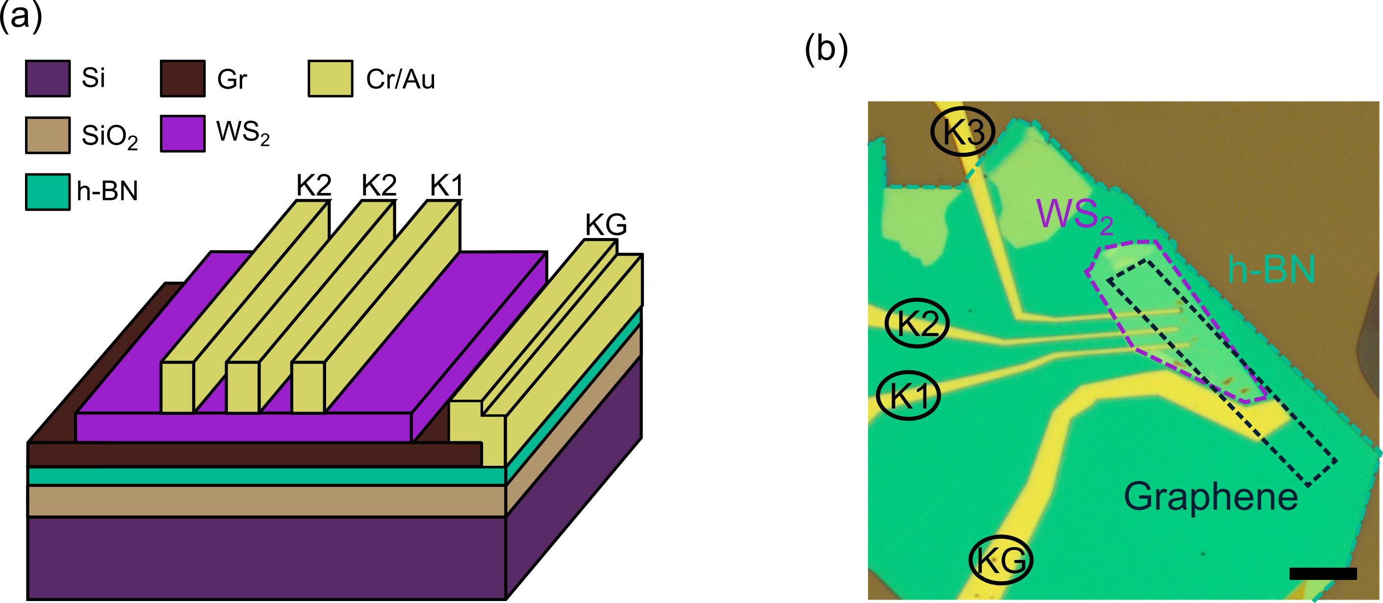
Devices with thin WS2 tunnel barriers have been fabricated by a van der Waals pick-up method using poly-carbonate (PC) films Zomer et al. (2014). A four-layer WS2 flake and a monolayer flake were chosen as tunneling barriers. The bottom electrode in the devices consists of a monolayer graphene, while for the top tunneling electrodes Cr/Au or graphite was deposited on the WS2 flakes. Moreover, we employ hexagonal boron nitride (h-BN) as bottom dielectric with a thickness of 40 nm. The flat h-BN substrates eliminate extrinsic disorder in graphene and WS2 Dean et al. (2010). Figure 1a and 1b show a schematic illustration of the 4L-WS2 device and an optical image of the heterostructure, respectively. All the measurements shown in the main text are data taken from the device with four layers of WS2 (D1), by using the KG-K1 tunneling electrodes (see Fig. 1). Data from the other electrodes can be found in the supplemental material section. The device with monolayer WS2 (D2) as barrier did not show any tunneling characteristics, an observation that is in-line with reports on monolayer MoS2 Josephson junctions, where metallic behavior in the monolayers was observed Island et al. (2016). Results from the D2 device can be found in the supplemental material.
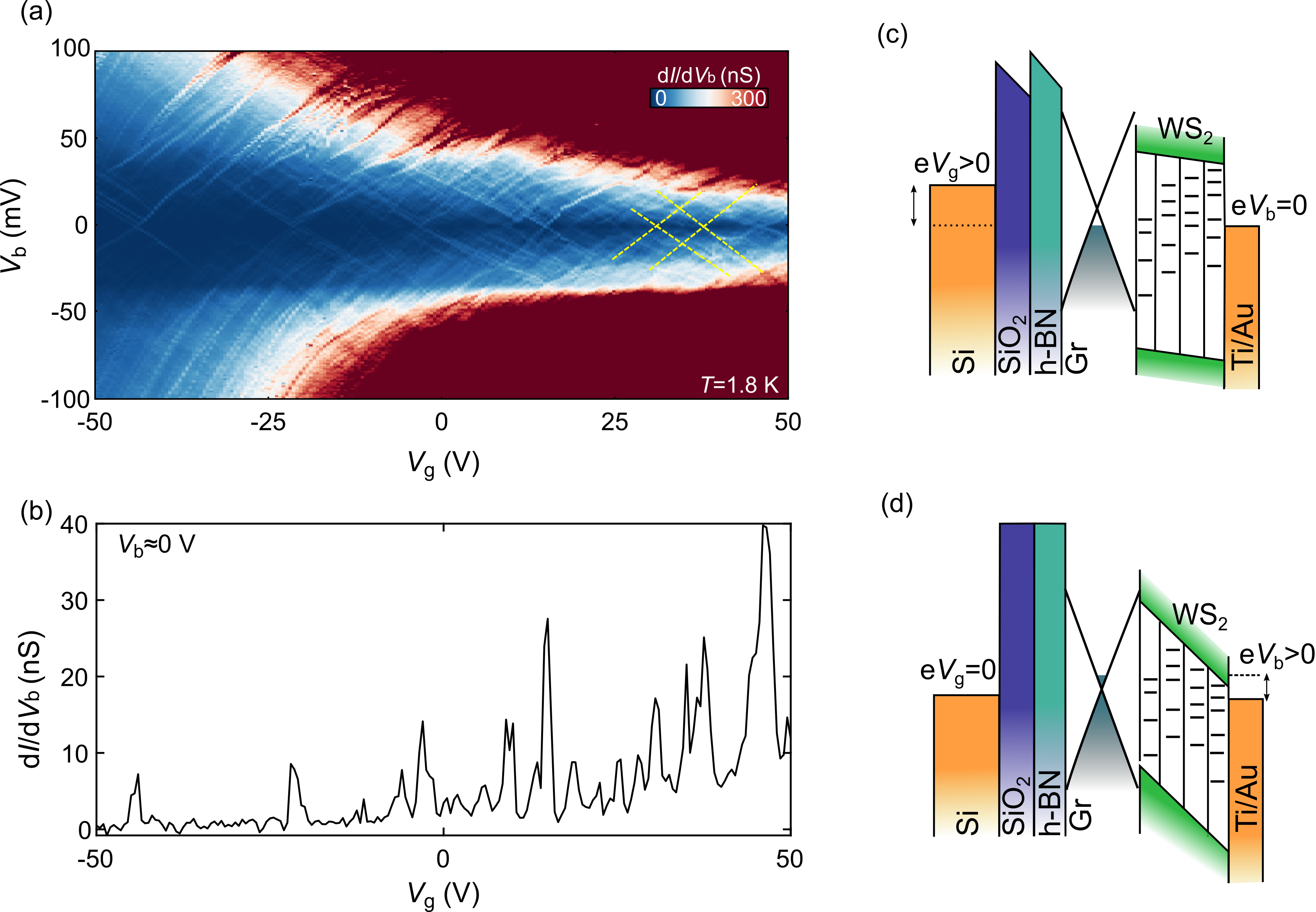
Figure 2a shows the dependence of the differential conductance () on the tunnel bias () and back-gate voltage () at a temperature of 1.8 K. Although at room temperature the conductance of the device is a few S (see Supplemental material), a significant decrease of three orders of magnitude in the values of , as well as many resonant features from Coulomb blockade effect are evident. The observed Coulomb diamonds in the differential conductance originate from parallel tunneling through multiple states originating from impurities in the WS2 layers (Fig. 2c), presumably sulfur or tungsten vacancies. Similar features in hexagonal boron nitride tunneling barriers have been reported recently (Chandni et al., 2016; Bretheau et al., 2017; Greenaway et al., 2018b; Liu et al., 2018). Moreover, an increase in the number of the resonances with back-gate voltage is observed (Fig. 2b), that can be attributed to the presence of localized states close to the edge of the conduction band, which could originate from sulfur vacancies similar to MoS2 McDonnell et al. (2014). Interestingly even at V, the zero-bias background conductance is suppressed, verifying that the Fermi level of WS2 is below the conduction band edge.
The conductance map in Fig. 2a provides further information about the nature of the localized states in the WS2 sheet. The full-width-at-half-maximum (FWHM) of the zero-bias peaks is found to be close to which suggests that the system is in the thermally broadened, weak coupling regime i.e. the electronic coupling to the impurity states is the smallest energy scale. Furthermore, from the slopes of the diamonds we can extract their capacitive couplings to the leads (, ) and the back gate () and can calculate the lever arm for the quantum dots Thijssen and der Zant (2008). We find that follows a distribution of values in the range of meV/V, with a maximum at 1.30.1 meV/V (see Fig. S2). Interestingly, we observe several diamonds with large values of at large negative gate-voltages. A possible origin of these diamonds are different types of impurities with a smaller localization size and on-site capacitance. Assuming that the level spacing is much smaller than the charging energy , such that the addition energy , we can estimate the size of the quantum dots using , for disk shape dots. Here is the electron charge, , the vacuum permittivity, is the dot radius and the effective relative permittivity of SiO2 and h-BN. Using the extracted values of meV, this assumption yields a quantum dot size of about 9-12 nm. It is worth to mention that the diamonds and their positions change significantly after thermally cycling the device (see Supplemental Material).
Above a voltage bias of 30 mV the conductance in the map of Fig. 2a increases significantly and many lines from diamonds can be observed. To explain such an increase of the current and the differential conductance at high bias, we have to take into account the effects of the interlayer voltage bias on the shape of the barriers. Although at zero bias and non zero gate voltage, the bias window contains only states within the band gap that assist the tunneling process (Fig. 2c), at higher bias the shape of tunneling barrier is modified and the WS2 conduction band is lowered Simmons (1963); Sarkar et al. (2015). This results in a field emission of the carriers above the band gap of WS2 (Fig. 2d) Georgiou et al. (2013); Sarkar et al. (2015), where carriers from the graphene and the electrode can tunnel directly into the WS2 layer, which increases the conductance significantly.
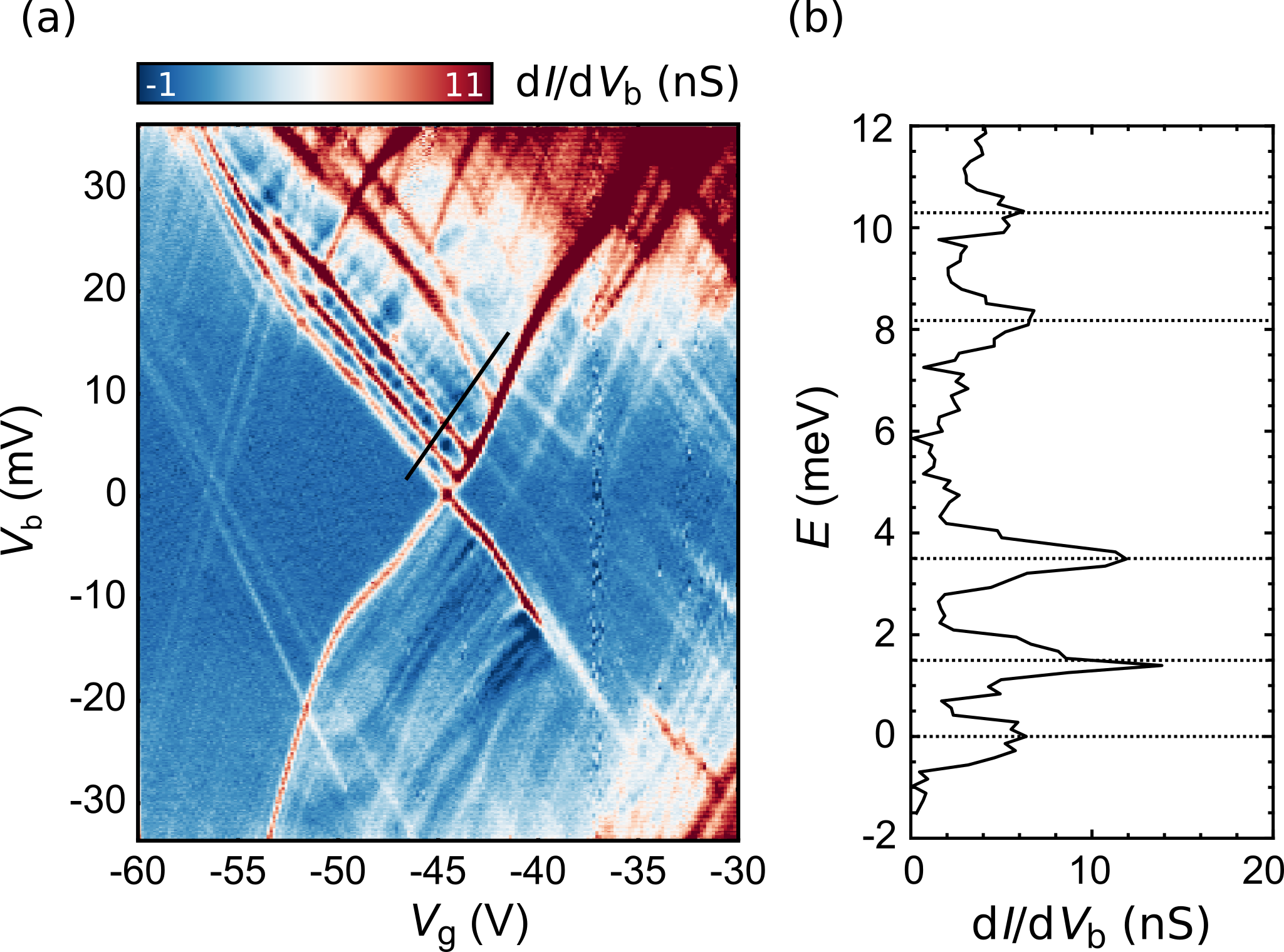
Figure 3a shows a detailed differential conductance map of the gate voltage regime between -60 and -20 V, where a clear Coulomb diamond can be observed. This particular diamond exhibits excited states for positive bias and many negative differential resistance (NDR) features in the sequential tunneling regime. Excited states can have many different origins and can be phonon, spin or orbital excited states. Figure 3b shows E vs. obtained from the line-cut of Fig. 3a (black line). The energy axis has been shifted such that the the ground state is at 0 meV for clarity. From this we can extract the excited state energies of the first two excited states which are 1.4 meV and 3.5 meV, respectively. The next pair of excited states have energies of 8.2 meV and 10.3 meV. It is worth mentioning that the diamonds, apart from providing information about the localized states in WS2, show features that originate from the graphene. In a few diamonds (like the one shown in Figure 4a), we observe lines with slopes that are different from those of the diamond edges. These lines represent multiple negative-differential-resistance (NDR) like feature. Earlier reports on molecular junctions using graphene electrodes Gehring et al. (2017) and tunneling spectroscopy through h-BN barriers Zihlmann et al. (2019), have shown similar lines in their stability diagrams and they have been attributed to universal conductance fluctuations (UCFs) from the graphene contacts.
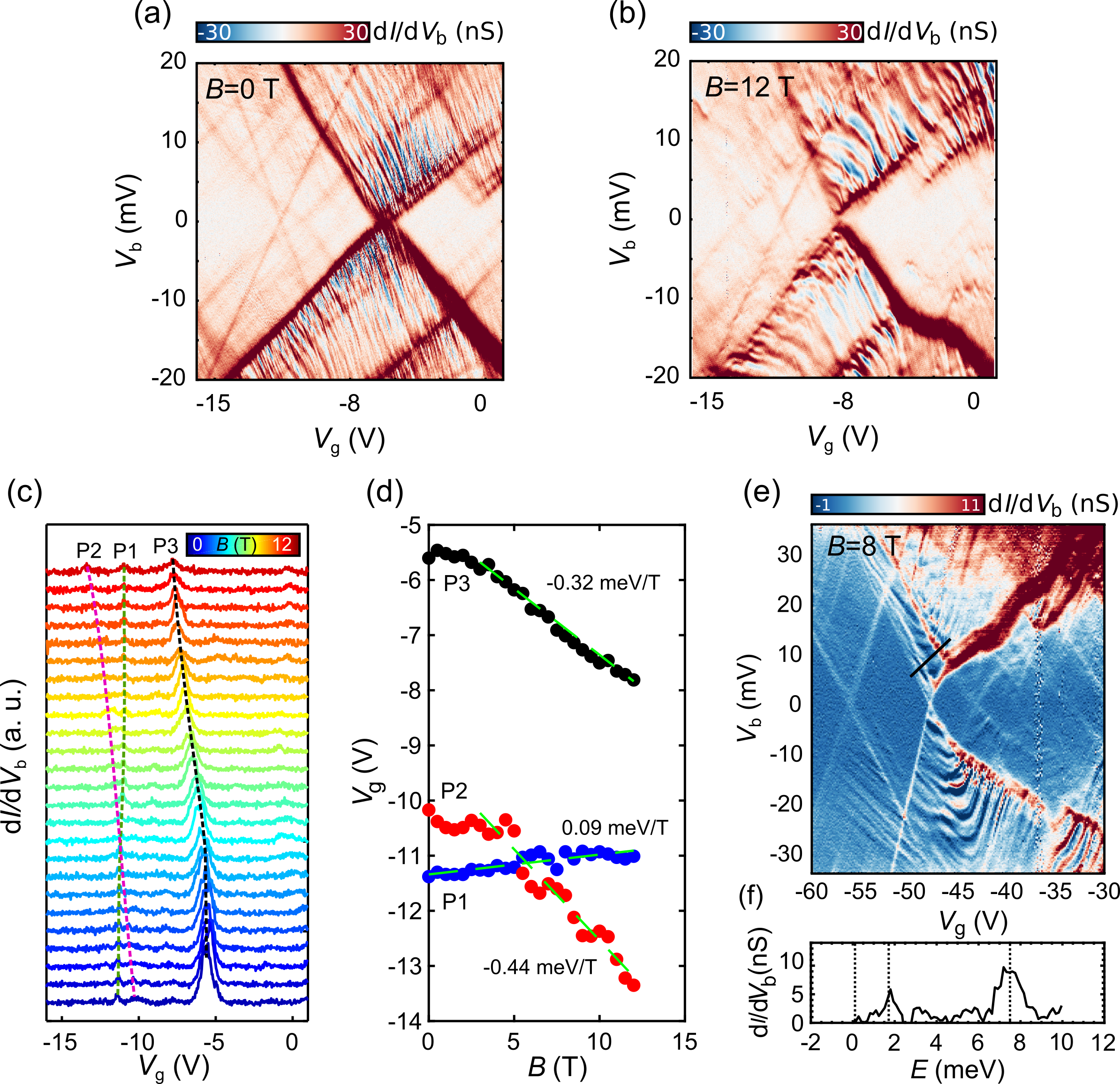
Upon application of a magnetic field perpendicular to the 2D plane, the Coulomb diamonds can reveal information about the spin and the orbital states. To this end we recorded the stability diagrams in the Fig. 3a and Fig. S1 at magnetic fields up to 12 T in order to study the field dependence of the ground and the excited states. Figure 4 shows the maps at 0 and 12 T, in (a) and (b), respectively. From the former, we observe clearly three zero-bias resonances, from which two have same values of (1.3 mV/V) while the other one has a slightly higher value of mV/V, presumably originating from a different type of defect. As it can be seen in Fig. 4b, the different types of diamonds have shifted horizontally at T, which can be explained by the coupling of the electron magnetic moment to the magnetic field. Moreover, the UCF lines decrease in number upon increasing due to the formation of Landau levels in the DOS of the graphene. Additionally, we observe bending of the excited state lines as well as the edges of the Coulomb diamonds, a finding which could be explained by strong capacitive coupling between multiple dots that contribute to transport.Hofheinz et al. (2006).
Figure 4c shows versus at zero bias, for magnetic fields from 0 to 12 T in steps of 0.5 T (blue to red). For T, the three ground-state resonance peaks are located at -7 V, -10 V and -11 V, which we label P1, P2 and P3, respectively. P1 and P3 have similar gate couplings, while P2 has a larger as was seen in Fig. 4a. The P2 and P3 peaks shift in a similar way to more negative energies with increasing magnetic field, indicating that the two states have the same orbital wave-function. The P1 peak, on the other hand, shifts weakly to more positive gate values. Such shifts of the three states, originate from the coupling of the magnetic moments of the localized states to the external magnetic field. This becomes apparent when plotting the peak positions of P1, P2 and P3 as a function of magnetic field (Figure 4 (d)). The field dependence of the P2 and P3 peaks is non-linear, indicating a strong orbital magnetic moment of the involved ground state. Furthermore, from the linear fit to the high magnetic field data of peaks P1, P2 and P3, we get magnetic moments of 0.090.03, 0.440.05 and 0.320.03 meV/T, respectively. From the Zeeman energy, , where is the Landé g-factor, and the magnetic moment and the Bohr magneton, g-factors 3.40.9, 15.81.8, 11.00.9. All the corresponding -factors are much larger than the value of 2 expected for a free electron. Thus, orbital magnetic moments play a significant role in the magnetic field dependent transport of defects in WS2.
Finally, we recorded the stability diagram shown in Fig. 3 at a magnetic field of 8 T (Fig. 4e). Besides the aforementioned bending of the excited state lines and the edges of the Coulomb diamond we observe a drastic change of the excited state energies when comparing the data recorded at 0 and 8 T: out of four lines observed at 0 T (see Fig. 3), we only observe two lines with energies 1.8 meV and 7.3 mV at 8 T (Fig. 4f). Such strong changes of the excited state energies further suggests that the corresponding factors are large and/or that the spin of the excited state is .
Unlike the hydrogen atom, whose ground-state has an orbital magnetic moment of zero () due to spherical symmetry, in the case of a dot formed in a 2D material there is a finite out-of-plane orbital magnetic moment even for the s-shell, as a result of the reduced dimension along the -axis. The orbital magnetic moment of a moving charge in a circular orbit, is given by Minot et al. (2004); Island et al. (2018): , where is the radius of the orbital, the Fermi velocity and the charge of the electron. Assuming a Fermi velocity around m/s, we obtain a radius for the P1, P2 and P3 resonances of 21, 92 and 61 nm, in relatively good agreement with the estimations of the dot size based on the capacitance extracted from the addition energies (Fig. 2a).
III Conclusions
In summary, we have performed tunneling spectroscopy measurements in van der Waals heterostructures with WS2 barriers. Our data reveal a rich spectrum of Coulomb diamonds that we attribute to localized states inside the WS2 sheet. These states localize carriers in a radius of 2-10 nm and show large orbital magnetic moments. Recent experiments indicate that such localized states have intrinsic spin-orbit coupling as large as 230 meV, and therefore tunneling devices as the ones shown here can be used for single spin-polarized electron injection. Lastly, localized states in TMDCs are important for single photon emission Aharonovich et al. (2016); Perebeinos (2015) and if properly engineered could provide new systems for quantum communications, similar to nitrogen-vacancy centers in diamond.
ACKNOWLEDGMENTS
This work is part of the Organization for Scientific Research (NWO) and the Ministry of Education, Culture, and Science (OCW). P.G. acknowledges a Marie Skłodowska-Curie Individual Fellowship under Grant TherSpinMol (ID: 748642) from the European Union’s Horizon 2020 research and innovation programme. Growth of hexagonal boron nitride crystals was supported by the Elemental Strategy Initiative conducted by the MEXT, Japan and the CREST (JPMJCR15F3), JST.
References
- Britnell et al. (2012) L. Britnell, R. V. Gorbachev, R. Jalil, B. D. Belle, F. Schedin, A. Mishchenko, T. Georgiou, M. I. Katsnelson, L. Eaves, S. V. Morozov, N. M. R. Peres, J. Leist, A. K. Geim, K. S. Novoselov, and L. A. Ponomarenko, Science 335, 947 (2012).
- Jang et al. (2017) J. Jang, H. M. Yoo, L. N. Pfeiffer, K. W. West, K. W. Baldwin, and R. C. Ashoori, Science 358, 901 (2017).
- Vdovin et al. (2016) E. E. Vdovin, A. Mishchenko, M. T. Greenaway, M. J. Zhu, D. Ghazaryan, A. Misra, Y. Cao, S. V. Morozov, O. Makarovsky, A. Patanè, G. J. Slotman, M. I. Katsnelson, A. K. Geim, K. S. Novoselov, and L. Eaves, Physical Review Letters 116 (2016), 10.1103/PhysRevLett.116.186603, arXiv:1512.02143 .
- de Vega and de Abajo (2017) S. de Vega and F. J. G. de Abajo, ACS Photonics 4, 2367 (2017).
- Ghazaryan et al. (2018) D. Ghazaryan, M. T. Greenaway, Z. Wang, V. H. Guarochico-Moreira, I. J. Vera-Marun, J. Yin, Y. Liao, S. V. Morozov, O. Kristanovski, A. I. Lichtenstein, M. I. Katsnelson, F. Withers, A. Mishchenko, L. Eaves, A. K. Geim, K. S. Novoselov, and A. Misra, Nature Electronics 1, 344 (2018).
- Wallbank et al. (2016) J. R. Wallbank, D. Ghazaryan, A. Misra, Y. Cao, J. S. Tu, B. A. Piot, M. Potemski, S. Pezzini, S. Wiedmann, U. Zeitler, T. L. M. Lane, S. V. Morozov, M. T. Greenaway, L. Eaves, A. K. Geim, V. I. Fal’ko, K. S. Novoselov, and A. Mishchenko, Science 353, 575 (2016), 27493182 .
- Eisenstein et al. (2017) J. Eisenstein, L. Pfeiffer, and K. West, Physical Review Letters 118 (2017), 10.1103/physrevlett.118.186801.
- Kim et al. (2018) K. Kim, N. Prasad, H. C. P. Movva, G. W. Burg, Y. Wang, S. Larentis, T. Taniguchi, K. Watanabe, L. F. Register, and E. Tutuc, Nano Letters 18, 5967 (2018).
- Becker et al. (2011) S. Becker, C. Karrasch, T. Mashoff, M. Pratzer, M. Liebmann, V. Meden, and M. Morgenstern, Physical Review Letters 106 (2011), 10.1103/PhysRevLett.106.156805.
- Chandni et al. (2016) U. Chandni, K. Watanabe, T. Taniguchi, and J. P. Eisenstein, Nano Letters 16, 7982 (2016).
- Greenaway et al. (2018a) M. T. Greenaway, E. E. Vdovin, D. Ghazaryan, A. Misra, A. Mishchenko, Y. Cao, Z. Wang, J. R. Wallbank, M. Holwill, Y. Khanin, S. V. Morozov, K. Watanabe, T. Taniguchi, O. Makarovsky, T. M. Fromhold, A. Patanè, A. K. Geim, V. I. Fal’ko, K. S. Novoselov, and L. Eaves, Communications Physics 1 (2018a), 10.1038/s42005-018-0097-1.
- Radisavljevic et al. (2011) B. Radisavljevic, A. Radenovic, J. Brivio, V. Giacometti, and A. Kis, Nature Nanotechnology 6, 147 (2011).
- Ovchinnikov et al. (2014) D. Ovchinnikov, A. Allain, Y.-S. Huang, D. Dumcenco, and A. Kis, ACS Nano 8, 8174 (2014).
- Lin et al. (2015) Y.-C. Lin, R. K. Ghosh, R. Addou, N. Lu, S. M. Eichfeld, H. Zhu, M.-Y. Li, X. Peng, M. J. Kim, L.-J. Li, R. M. Wallace, S. Datta, and J. A. Robinson, Nature Communications 6 (2015), 10.1038/ncomms8311.
- Georgiou et al. (2013) T. Georgiou, R. Jalil, B. D. Belle, L. Britnell, R. V. Gorbachev, S. V. Morozov, Y.-J. Kim, A. Gholinia, S. J. Haigh, O. Makarovsky, L. Eaves, L. A. Ponomarenko, A. K. Geim, K. S. Novoselov, and A. Mishchenko, Nature Nanotechnology 8, 100 (2013).
- Kretinin et al. (2014) A. V. Kretinin, Y. Cao, J. S. Tu, G. L. Yu, R. Jalil, K. S. Novoselov, S. J. Haigh, A. Gholinia, A. Mishchenko, M. Lozada, T. Georgiou, C. R. Woods, F. Withers, P. Blake, G. Eda, A. Wirsig, C. Hucho, K. Watanabe, T. Taniguchi, A. K. Geim, and R. V. Gorbachev, Nano Letters 14, 3270 (2014).
- Dvir et al. (2018) T. Dvir, F. Massee, L. Attias, M. Khodas, M. Aprili, C. H. L. Quay, and H. Steinberg, Nature Communications 9 (2018), 10.1038/s41467-018-03000-w.
- Li et al. (2017) X.-G. Li, Y.-P. Wang, J. N. Fry, X.-G. Zhang, and H.-P. Cheng, Journal of Physics and Chemistry of Solids (2017), 10.1016/j.jpcs.2017.12.005.
- Avsar et al. (2014) A. Avsar, J. Y. Tan, T. Taychatanapat, J. Balakrishnan, G. Koon, Y. Yeo, J. Lahiri, A. Carvalho, A. S. Rodin, E. O’Farrell, G. Eda, A. H. C. Neto, and B. Özyilmaz, Nature Communications 5 (2014), 10.1038/ncomms5875.
- Raja et al. (2017) A. Raja, A. Chaves, J. Yu, G. Arefe, H. M. Hill, A. F. Rigosi, T. C. Berkelbach, P. Nagler, C. Schüller, T. Korn, C. Nuckolls, J. Hone, L. E. Brus, T. F. Heinz, D. R. Reichman, and A. Chernikov, Nature Communications 8, 15251 (2017).
- Song et al. (2015) X.-X. Song, Z.-Z. Zhang, J. You, D. Liu, H.-O. Li, G. Cao, M. Xiao, and G.-P. Guo, Scientific Reports 5 (2015), 10.1038/srep16113.
- Zomer et al. (2014) P. J. Zomer, M. H. D. Guimarães, J. C. Brant, N. Tombros, and B. J. van Wees, Applied Physics Letters 105, 013101 (2014), arXiv:1403.0399 .
- Dean et al. (2010) C. R. Dean, A. F. Young, I. Meric, C. Lee, L. Wang, S. Sorgenfrei, K. Watanabe, T. Taniguchi, P. Kim, K. L. Shepard, and J. Hone, Nature Nanotechnology 5, 722 (2010).
- Island et al. (2016) J. O. Island, G. A. Steele, H. S. J. van der Zant, and A. Castellanos-Gomez, 2D Materials 3, 031002 (2016).
- Bretheau et al. (2017) L. Bretheau, J. I.-J. Wang, R. Pisoni, K. Watanabe, T. Taniguchi, and P. Jarillo-Herrero, Nature Physics 13, 756 (2017).
- Greenaway et al. (2018b) M. T. Greenaway, E. E. Vdovin, D. Ghazaryan, A. Misra, A. Mishchenko, Y. Cao, Z. Wang, J. R. Wallbank, M. Holwill, Y. Khanin, S. V. Morozov, K. Watanabe, T. Taniguchi, O. Makarovsky, T. M. Fromhold, A. Patanè, A. K. Geim, V. I. Fal’ko, K. S. Novoselov, and L. Eaves, Communications Physics 1 (2018b), 10.1038/s42005-018-0097-1.
- Liu et al. (2018) Y. Liu, Z. Tan, M. Kumar, T. S. Abhilash, G. jun Liu, and P. Hakonen, APL Materials 6, 091102 (2018).
- McDonnell et al. (2014) S. McDonnell, R. Addou, C. Buie, R. M. Wallace, and C. L. Hinkle, ACS Nano 8, 2880 (2014).
- Thijssen and der Zant (2008) J. M. Thijssen and H. S. J. V. der Zant, physica status solidi (b) 245, 1455 (2008).
- Simmons (1963) J. G. Simmons, Journal of Applied Physics 34, 1793 (1963).
- Sarkar et al. (2015) D. Sarkar, X. Xie, W. Liu, W. Cao, J. Kang, Y. Gong, S. Kraemer, P. M. Ajayan, and K. Banerjee, Nature 526, 91 (2015).
- Gehring et al. (2017) P. Gehring, J. K. Sowa, J. Cremers, Q. Wu, H. Sadeghi, Y. Sheng, J. H. Warner, C. J. Lambert, G. A. D. Briggs, and J. A. Mol, ACS Nano 11, 5325 (2017).
- Zihlmann et al. (2019) S. Zihlmann, P. Makk, S. Castilla, J. Gramich, K. Thodkar, S. Caneva, R. Wang, S. Hofmann, and C. Schönenberger, Physical Review B 99 (2019), 10.1103/physrevb.99.075419.
- Hofheinz et al. (2006) M. Hofheinz, X. Jehl, M. Sanquer, G. Molas, M. Vinet, and S. Deleonibus, The European Physical Journal B 54, 299 (2006).
- Minot et al. (2004) E. D. Minot, Y. Yaish, V. Sazonova, and P. L. McEuen, Nature 428, 536 (2004).
- Island et al. (2018) J. O. Island, M. Ostermann, L. Aspitarte, E. D. Minot, D. Varsano, E. Molinari, M. Rontani, and G. A. Steele, Physical Review Letters 121 (2018), 10.1103/PhysRevLett.121.127704.
- Aharonovich et al. (2016) I. Aharonovich, D. Englund, and M. Toth, Nature Photonics 10, 631 (2016).
- Perebeinos (2015) V. Perebeinos, Nature Nanotechnology 10, 485 (2015).